
Common AXI Themes on Xilinx's Forum
Xilinx has committed their infrastructure to AXI. Zynq’s are built around AXI3, while most of the Vivado generated infrastructure within their FPGA environment is now AXI4. As we’ve examined on this forum, their training materials will lead you to either a broken demonstration AXI-lite slave design, or a broken AXI (full) slave design. Both of these designs will hang your bus if the bugs within them are ever triggered. As of Vivado 2020.2, these bugs have yet to be fixed. (You can find better, working examples of an AXI4-lite slave design here, or a working AXI4 full slave design here).
AXI is also ARM’s published bus standard. The popularity of placing a ARM CPUs within custom SoCs has helped to make this standard ubiquitous.
While I have filed bug reports in 2017 and 2018 on Xiling’s forums regarding these broken demonstration designs, Xilinx has yet to fix their designs as of Vivado 2020.2. [1], [2] Indeed, at this point, it’s not clear if Xilinx will ever fix their demonstration designs. Perhaps I shouldn’t complain–their broken designs simply make the services I offer and sell that much more valuable.
In the meantime, however, I have been browsing Xilinx’s forums to see if I can help individuals working struggling to get their designs to work with AXI. My one claim to fame? I have now formally verified several AXI and AXI-lite designs. From this claim alone, I hoped to demonstrate myself qualified to comment on problems Xilinx users might have.
Along the way, I’ve had mixed success. I’ve formally verified several user designs, and I’ve tried formally verifying several of Xilinx’s IP designs. Sometimes I’ve been successful, and so I’ve found bugs in their AXI Ethernet-lite core and verified that there were no bugs in either their AXI GPIO or their AXI Block RAM Controller (limited bounded model checks only). Neither was I able to find any bugs in their demonstration AXI or AXI-lite masters. (Their AXI stream master, on the other hand …) Other designs, however, such as their datamover, their interconnect, their Avalon to AXI bridge, their AXI firewall, or even their AXI timer all depend on encrypted IP components, and so I have been unable to verify them or comment on their internal operations and details.
Still, I thought it might be worth taking some time to look at a sample of the Xilinx forum threads I’ve contributed to which have discussed AXI. Yes, this sample set is biased: it’s a subset of only those posts I’ve contributed to. Still, I’ve tried to be active in as many AXI issues as I could have, and so I have at least convinced myself that this is a representative sampling of AXI problems Xilinx users have come across.
Getting started
The first problem beginning AXI users tend to come across is finding an easy how-to discussion or example. This user, for example, was looking for instructions on how to design a custom AXI master. Here, another user is asking for an AXI Hello world equivalent? The best answer I have to these questions is to offer my EasyAxil design as a starting point for learning how to build an AXI-lite slave design.
In general, however, Xilinx’s answer to the getting started problem is to offer one of three basic approaches of relatively increasing complexity:
 |
-
Use Xilinx’s AXI GPIO controller. This provides an easy on-ramp for an engineer to control digital logic by controlling wires within the design. This approach is quite easy, and it sounds great. It sounds great, that is, until you start reading the various user experiences among those who have used this approach. This user, for example, measured his GPIO toggling perfromance at 3.8MHz. Another user measured a cycle time of 120ns per instruction when accessing his AXI-lite peripheral from a 100MHz clock. These are both kind of slow, given that the ZipCPU can toggle a GPIO at 47MHz when starting from a 100MHz clock, but that’s really another story.
The bottom line here, however, is that while the approach works–it’s really not the way to achieve high speed communication between your CPU and the rest of your design. CPUs just aren’t designed to toggle GPIO registers at high speeds. (We’ll ignore the fact that Xilinx’s AXI GPIO device requires a minimum of four clocks per access, together with the inherent latency in their interconnect–or even any interconnect for that matter, and …)
-
Their second recommendation is that you start with Xilinx’s AXI block RAM controller, and then connect both this controller and your design to a shared block RAM. This will get you closer to an ability to adjust registers within a design, but it only offers the ability to read and write a shared RAM–not to read and write control registers within a design, which is a common usage model. I mean, how do you tell your programming logic (PL) that new data is in the block RAM, or that it should start processing that data? A second problem with this approach is that there’s no way to stall something until your design is ready or a previous task has completed. This could easily reduce a CPU to polling for results that might otherwise be accomplished in a clock or two.
-
The third approach is often the recommended one: request Vivado create a demonstration AXI design for you, and then modify that design to meet your needs. This is certainly Xilinx’s recommended approach. [1], [2]
The problem with this third approach is that Xilinx’s demonstration designs are quite broken.
-
Here’s a list of links to forum posts regarding user designs that have been broken by using (what appears to be) Xilinx’s AXI-lite slave demonstration design:
Even with these bugs, many Xilinx user’s would much rather just blindly trusting Xilinx’s broken designs based upon a faulty appeal to authority. Much to my surprise, some individuals have even found my easy example to be too complicated.
-
Here’s a similar list to posts about Xilinx’s demonstration AXI full slave: 1, 2, 3
These actually follow a common pattern, where a user will complain of one problem yet subsequent analysis then reveals another problem within.
Sadly, while I can often find bugs in user designs when they are posted, a common theme is that of someone with a design bug, but where they cannot share their AXI slave component. Without any RTL to work off of, these bugs can be hard to find.
Another recent complaint was that Xilinx’s demo design only gets 50% read throughput. Yes, this was also one of the problems I discovered with a formal examination of their AXI full design. It’s a bit of a shame too, since AXI was supposed to be designed as a high performance bus, to find so many example designs that can’t achieve high performance.
As always, be careful who you trust. Not every demonstration design someone will recommend to you works. One poster, [larshb] had a design he’d used successfully for years. When he recommended it to another, I was able to run a formal proof of it and discover many of the same bugs within it that others had complained of above. I wouldn’t hold it against him now, though. My bet is the next time he makes such a recommendation he’ll have fixed his bugs. My worry is more about those who are still unaware that Xilinx’s demo designs are buggy–just like [larshb] used to be.
If you want a better design to start from, you should consider this Easy AXI-lite design, and even the associated register handling check. Alternatively, Analog Devices posts a nice AXI-lite design that I’ve seen a couple designs built from as well. While that one works nicely, it’s not setup within for a formal proof. How then will you know if any changes you make to the design break it? (You won’t.)
Either example, however, should help you get started.
Debugging AXI components
A second reoccurring theme centers around how should one go about debugging AXI components. Of all things, debugging AXI components should be easy. There are three basic steps involved.
 |
-
Formally verify your AXI component.
If you haven’t tried verifying an AXI4 design before, then you should know that it is really easy to do for an AXI-lite component: Just instantiate these AXI-lite slave properties, and then apply SymbiYosys to your design.
AXI (full) designs are a bit more complicated, but I provide AXI4 properties, examples and a bit of instruction to my Patreon supporters, so those are still quite doable as well.
I should also point out that, of all the logic that can be formally verified, bus logic tends to be some of the easiest to verify. It’s also some of the most critical logic within a design. Consider, for example, what would happen if a single component failed to follow the rules of the bus: the entire design will likely lock up. On the other hand, if that component follows the rules of the bus but just failed to do what it was designed to do, you might still manage to recover the rest of the design–at least enough to use your design to debug what’s going on. The point here is, getting your bus logic right is critical to debugging the application you are really interested in.
While many individuals would recommend building a simulation test bench to stimulate your brand new component in a simulation environment, you should be aware that the AXI Verification IP offered by Xilinx isn’t known for triggering the bugs within their own designs–or surely they would’ve never published them in the first place.
-
Once you’ve formally verified your design, the next step is to place your component into an integrated design simulation, and verify that it works together with the other components of your design.
As I mentioned above, be careful with Xilinx’s AXI Verification IP. It won’t necessarily trigger any of the bugs within their designs. To my knowledge, this isn’t unique to Xilinx either. On one contract I’m working on, with a custom AXI Verification IP, the AXI VIP has the exact same problem. The problem itself is rooted in the fact that the bugs are often triggered by a busy interconnect–something rarely simulated when the design is examined in isolation.
That leads to the real difficult part of simulation: testing your design in a sufficiently complex environment–such as with the Processing System (PS) of the Zynq attached. While I’ll admit that I’m still looking for a good way to do this reasonably, I can also share that I rarely have any problems with formally verified designs not working when integrated into larger environments.
-
Connect your design to actual hardware and try it out.
This should only ever be the third method you try, not the first. Sadly, this becomes the method many individuals end up using to debug their designs. Given that many of the bugs listed in the previous section will hang the entire system, and worse that Xilinx’s AXI Verification IP isn’t known for triggering these bugs in simulation, users who take this road often find themselves struggling to figure out where their design actually failed.
The result is that there are a lot of forum requests for help debugging custom IPs. See for example, [1], [2], [3], [4], [5], [6], or [7].
Here are some forum posts from users requesting simulation help: [1], [2], [3]. One person even asked about a technique dear to my heart–formal methods, although these tend to only rarely be discussed on the forum.
Here’s another crazy one: in this case, the user didn’t want a full fledged AXI test. He believed he could perform a sufficient test in hardware. While I’ll admit to having been there before, the cost of debugging in hardware is a lot of pain. Worse, a piece of hardware might appear to work for weeks or months on end, only to have an undetected and latent bug lying within it. (That was my case with my own SDRAM controller, before I formally verified it.) Finding and fixing such bugs can be even more challenging when they don’t present themselves often. This is not a path I would recommend, therefore, if you can avoid it.
 |
One piece of advice I often offer to users forced to do their debugging in hardware is to connect an AXI firewall to a design. This can be useful when trying to determine whether the fault is your own, or Xilinx’s AXI infrastructure. If the fault occurs with the firewall in place, then the fault must lie somewhere else in your design (or you didn’t wire it up right). Even better, the firewall will provide a fault signal which you can use to trigger an internal logic analyzer to capture what’s going on. The technique isn’t perfect, however, as the AXI firewall I have modifies the environment it is observing–so it is possible to pass the firewall test while still having a bug within your design. (Doh!)
Custom AXI masters
The problem isn’t limited to the design of AXI slaves. Many users have also written in with problems debugging their custom AXI masters as well. Examples include: messing up AXI handshaking, not knowing how to set up a master to handle arbitrary burst lengths, needing help just getting started with building an AXI master, and just not handling AXI outputs per spec. Beware that your problem might not just be the master at fault. In this example the master was producing a wider ID field than the interconnect was expecting.
Some of these problems we’ve discussed on this blog, although I’ll admit to being rather light on how to generate burst-capable AXI masters. Still, I have posted how to build a generic AXI(lite) master, and again on the problems associated with building a burst-capable AXI master. If the Lord wills, we may even discuss a new AXI4 memory unit for the ZipCPU that I’ve been working on recently.
Another common AXI problem is specifying the length of an AXI burst in AxLEN, rather than one less than the burst’s length. Although I have only one link for this, I’m still going to declare it to be a common problem if for no other reason than it’s one I’ve struggled with myself. Not only that, this is one of the first things I look for when attempting to debug someone else’s design: do the number of requests match the number of responses? For this, it helps to have the computer help count, and so either a good AXI VIP or an AXI firewall can also be useful here.
Out-of-protocol designs
Sadly, there’s only so much you can do for the user who hasn’t done their reading on how AXI is supposed to work. Often these individuals can get their design to work with the AXI VIP suite, or perhaps with one or two peripherals, or one implementation of the AXI interconnect. The moment their environment changes, however, their design then breaks. Some of these users will then even go so far as to blame every one nearby when the failure was actually to be found within their non-protocol compliant implementation in the first place.
As one example, the AXI4 specification is very clear that AWVALID is not
allowed to wait on WREADY and vice versa, and yet users will still create
designs where they expect one transaction, whether AW or W, to take place
before the other.
[1],
[2],
[3]
The problem is generally compounded by the fact that few AXI slave substitutes
act like the MIG AXI slave individuals ultimately want to use. Therefore, once
they verify their core against a generic AXI slave–perhaps even the VIP–they
often pick up a bad habit along the way.
 |
I should also point out that this isn’t just a beginning user mistake either,
since Xilinx made a very similar mistake in their AXI Ethernet-lite
controller
of not setting RVALID unless RREADY was already set.
Not every problem is so obvious. This user set a valid signal on the clock immediately following a reset, not realizing that this would violate the specification. Indeed, I might argue that the AXI4 specification isn’t very clear on this issue–a figure alone is used to explain it with a bare minimum of accompanying text. (See Fig. A3-1 on page A3-36 in this copy of the spec.)
As with any bus protocol, you need to know when a request is made. This
follows from the requirement that there must be one response for every
request. An AXI request, for example, is made any time xVALID && xREADY
are true on the same clock cycle. Moreover, if xVALID && !xREADY, the
request needs to be held into the next cycle. This
user,
however, didn’t see a problem with holding AWVALID high until his request
had been made and then dropping it when AWREADY was low. Breaking the
protocol in this fashion will also break valid AXI components. Not all
components ignore bus signals when xVALID && !xREADY. Many components I’ve
come across, such as Xilinx’s
GPIO
or even their IPIF register handler as just two examples,
accomplish their internal task before setting xREADY to accept the request
for that task. In other words, these designs, those that depend upon them,
and many other AXI slave designs will start working on the request before
they accept the request in the first place.
Finally, there was one user who assigned meaning to AXI ID’s coming from his
master. If I recall, he was attempting to send side-channel information in the
ID bits–something probably more appropriately left for the xUSER bits.
This user was then disappointed to discover that the AXI width converter didn’t
preserve AXI ID’s. [1] Had he stuck with
the rules of the bus, instead of trying to use an undocumented feature, he
wouldn’t have needed to try to rearrange his design when the feature he wanted
was suddenly no longer implemented.
Throughput, throughput, throughput!
Much to my surprise, when I started tallying these forum posts together, there were a lot of requests for help achieving higher AXI throughput. Perhaps this shouldn’t surprise anyone. One of the main purposes of custom digital logic in the first place is to implement complex algorithms which can’t be done in real time on a high powered CPU. One of the things that is often missed, however, is that high powered CPUs have carefully designed high speed bus implementations. How shall FPGA designs built upon AXI compete?
 |
Yes, AXI was designed to be a high performance bus. That doesn’t mean that every implementation will achieve that high performance. Indeed, there have been a lot of requests for help to achieve higher throughput, or complaints about the throughput provided by Xilinx’s infrastructure. Here are just a few of those: [1], [2], [3], [4], [5], [6], [7], [8], [9], [10], [11].
I was a bit surprised to discover that the PS (i.e. ARM’s CPU) doesn’t automatically communicate using bursts with the Programming Logic (PL), but rather needs to be set up for that purpose. When you think about it, however, it makes sense. If the design hadn’t been built that way, then you might find yourself accidentally reading from a peripheral where reads also cause side effects not normally present when simply reading from a memory. Still, it’s worth remembering.
But let’s start at the top. If you want high throughput through your AXI subsystem, then there are some very specific things you can and should be doing:
 |
-
Use a common clock across all components if possible. Crossing from one domain to another will add at least two clocks of latency from each domain. It will also slow your bus down to the speed of the slowest clock.
-
Avoid width conversions by using a common width for your data bus. Even the most basic width conversion will add two clocks of latency to your design. More complicated conversions, or converters designed to be generic will likely take more latency. For example, even my own AXI downsizer takes two clocks to process an incoming write request, and another clock (or two) on the return.
-
If possible, use the maximum data width you can for this purpose–but make it common across all bus components.
In one case, a user connected their 32-bit design to the 128-bit port of the ARM (PS). They were then disappointed to discover that a 32-bit request from the ARM was coming into the bus at 128-bits (no surprise there), but then being converted into four independent 32-bit requests–one valid one and three empty requests! (In the after-analysis, this may have been a result of the PS configuration getting out of sync with the RTL design.)
It’s not just throughput that’s at issue. This user complained of too much latency in the interconnect, and this one was looking for a strategy to achieve low latency access. Indeed, latency and throughput are both related performance numbers.
 |
Finally, as with all optimization tasks, your first step will be to get the design to work slowly, your second step will be to measure your performance, and then your third step will be to do any actual optimizations. That leads to this discussion of how to measure throughput. There was also this question about how to measure the throughput to memory within an FPGA.
I also have an approach I hope to write about soon for measuring AXI throughput. It’s built around this basic throughput measuring AXI-lite slave. The slave examines AXI (full) bursts and makes measurements of the bus it can snoop on. From this information, I should be able to measure bus throughput and latency–but that’s a project for another day.
Don’t expect too much from software running on the PS either. I’ve seen a
couple of users asking what it would take to get a software memcpy() to run
using burst mode. How then shall a user command an AXI burst from
software?
(with links 1
and 2) As I mentioned above, the bottom line
answer is … you can’t.
This follows from the nature of how CPUs work. CPUs execute instructions. They don’t execute bursts of instructions, but singular instructions. Hence, if you have a software loop to read a string, the CPU doesn’t know to issue a burst. It only knows each instruction individually. To make matters worse, if any read instruction receives a bus error, the CPU needs to stop on a dime at that instruction without issuing any further memory accesses or updating any further registers. That makes burst memory handling challenging at best.
One potential solution is to tell the CPU that the memory address range in question is cachable, and then to read it into the cache since cache reads can be done in bursts. This has other problems, however, since you might accidentally read peripheral memory you didn’t intend to read as a result of reading an entire cache line. The bottom line here is that if it looks like memory, you might be able to cache it and get burst access. If not, you’ll either need a DMA or be stuck with singleton reads and writes.
AXI Datamover Bugs
 |
A second topic that surprised me due to its prevalence was the number of issues surrounding Xilinx’s Datamovers (DMAs). Xilinx provides three basic datamovers: a memory to memory DMA sometimes called MM2MM, a memory to stream DMA (MM2S), and a stream to memory DMA (S2MM). They also provide other similar cores to include their centralized DMA (CDMA) and Video DMA (VDMA) controllers. Sure enough, they’re all encrypted, or I would’ve run a formal check on them given all the controversy surrounding the S2MM datamover in particular.
Since we’ve just discussed AXI performance, it follows that the official answer to achieving high performance on an AXI bus is to use a datamover (DMA) for high speed memory transfer. The good news is that these vendor provided data movers are indeed high speed, full of features, and provided with a tutorial on how to do DMA transfers. In particular, these DMAs are some of the few vendor supplied AXI masters that will use the full AXI burst capability. Even better, many user tasks can be placed nicely between an AXI MM2S and an S2MM, leaving the vendor tools to handle all of the complicated data movement processing. What more could you want?
The problem here seems to stem from certain non-intuitive S2MM design features found in Xilinx’s deesign. Whether or not these are actually bugs appears to be a matter of debate, but their S2MM design clearly doesn’t do what many users are expecting.
I have not personally used Xilinx’s S2MM design, so I’m more of a witness and idea pollinator regarding it than anything else. That said, I have built (and formally verified) my own S2MM DMA, and I can assure you that mine does not have these non-intuitive features.
What non-intuitive features am I talking about? Well, first, the S2MM design
will stop its transfer upon receiving a TLAST signal. I’m told this feature
was created to support network packets, where the full length of the packet
might not be known until the end of the packet. The second problem is that
without the TLAST signal, the S2MM design will hang while waiting for it.
If that weren’t enough, users need to prevent the S2MM component from receiving
any stream data prior to being configured with a transfer length, destination
address, and a command to start transferring. Failing to prevent data from
entering prior to configuration will cause the S2MM design to hang. Or, at
least, this is what I’ve managed to learn from the various S2MM posts I’ve
been watching.
Here are just some of these S2MM posts that I’ve come across:
-
DMA transfer fails (No solution identified)
-
S2MM sometimes runs and works, other times just fails and trashes the SDK
Like I said, however, the official answer is that this S2MM design is bug free. Your mileage, however, might vary.
You are, of course, welcome to use my own S2MM controller if you would rather. It is available for free under the Apache license. It has worked nicely for some users. However, unlike Xilinx’s controller, mine doesn’t come with any Linux kernel or other software drivers. At the same time, it doesn’t have the surprising features either.
Resetting DMA
Before I move on to the smaller categories, there is one large theme left and that is the problem associated with resetting an AXI DMA. Indeed, this problem has been such an issue that I’ve written two posts on the topic–I’ll get to those in a moment. The general problem here seems to be either that users just naturally want to reset the DMA between bursts, or that somehow the DMA gets hung and so they want to reset things and start over.
 |
Why might your DMA hang? Perhaps because you’ve copied one of Xilinx’s demonstration designs and you are trying to copy data from it? That’s a common theme through this section, but also a theme I’ve rarely been able to prove. Perhaps the DMA failed because of the bugs in the demonstration designs. Perhaps it failed because an off-chip interface hung when the chip it was talking to went off line. Perhaps something else went wrong with either the DMA or the AXI infrastructure and now the user wants to reset the DMA. [1] The problem, however, is that the user typically wants to reset the DMA without resetting the rest of his design.
This is a problem in AXI, since AXI has no mechanism to abort an ongoing transaction simply because the master is no longer interested in either continuing it or receiving the results from it.
 |
The first post I wrote to address this problem was my post discussing protocol firewalls. If the problem is caused by a misbehaving user peripheral, a firewall should fix the problem. The firewall would guarantee that all AXI requests get responses, and that (following any protocol error) the DMA gets an appropriate bus error response. Even better, my own firewalls can be configured to reset the downstream slave, and so allow you to recover from a failure should one ever happen.
 |
The second post discussed the difficulty of resetting an AXI
component such as a DMA.
The problem, as mentioned above, is that you need to continue to provide any
write data that you’ve committed to, and you need to continue to wait for any
writes or reads to complete before you can declare a component idle. That
also means that you need to leave RREADY and BREADY high during this time,
and further that you need to know how many responses are outstanding. This
is quite doable if the core was designed properly with a transaction abort
function, but such a function is fundamentally very different from a soft
reset. That’s the good news. The bad news is that there’s no way to recover
from a non-compliant slave apart from using a
firewall–otherwise
your design may well hang until the next reset.
-
Short resets reset the DMA, long ones don’t. This is probably another example of looking for the bug in the wrong place. The underlying bug was associated with properly engineering separate reset domains, but that wasn’t apparent from the original question.
-
User reports a design lock up when the downstream hiccups and takes too long to respond. Unfortunately, even with some help from an official Xilinx representative, this issue was never resolved to know what the root cause was.
-
Resetting S2MM, but not the rest of the design. This looks like the S2MM problem above, where the S2MM was given data before being configured. (But
TREADYwas high …?) This was then compounded when the user tried to recover his design by resetting his S2MM component and not the rest of the design. -
Resetting between every pair of transactions. This user felt that it was appropriate to reset the S2MM core between every usage. Such resets should never be required. In reality, his underlying problem was probably the
TREADYbug listed above. -
Software resets hang the DMA. This follows from our discussion above. It also appears that this user complained about the same issue twice.
-
How do you reset the AXI DMA IP? This user was looking for a guaranteed way to restart the AXI DMA from software from scratch. He was looking for a failsafe way to do this. The problem is that, if your FPGA logic is hanging the DMA, there may be no hardware way to reset the design without resetting the entire design.
The bottom line answer remains the same as before: 1) formally verify everything that touches your bus, 2) Simulate everything before placing it onto your hardware, and 3) use logic analyzers if necessary if you are struggling with any problems afterwards. If you do find hardware bugs in step three, that’s a sign you messed up steps 1 and 2. Go back and re-do those better, so they won’t have the same problems again in the future.
If you can’t simulate an ARM CPU, then get a digital design with a CPU within it that you can simulate.
FFT IP core
FFT questions aren’t really AXI questions, but they aren’t all that uncommon either. Indeed, FFT questions are common enough that we’ve discussed how to solve FFT problems in general already, as well as how to handle in-hardware protocol testing with an AXI-stream based component. Both approaches should help the users below get closer to their solution.
-
The FFT core hangs. From a forum question standpoint, this one was horrible. The user provided a vague description of something going wrong, but then provided no other information suitable for narrowing the problem down. In the end, the user explained the issue by stating that there was an AXI protocol error of some unspecified type.
-
What is the FFT IP core’s pipeline latency? This question confused me. Why not just measure it? Any good simulation should be able to provide this answer. This leaves me wondering if the user didn’t simulate his design before moving to hardware, and so had no hard insight into how the design was actually working now that he had placed it onto his hardware.
Cache coherency
When working with a CPU, always be aware of the issue of cache coherency. It’s not uncommon to use a DMA to transfer data and then, only later, to discover that the DMA has changed data within the CPU cache. I know I’ve had that problem when working with the ZipCPU. That also appears to be the problem this user was struggling from.
How to debug an AXI4 interconnect?
It wasn’t clear from this post if the user wanted to verify their own interconnect, or one they built on their own.
Personally, I would recommend formal verification. That said, my own AXI interconnect has been failing its formal proof for some time (while passing simulation tests), so … I have some work to do here in my own back yard.
Failing to provide a full 16-clock reset
This one isn’t quite as simple as my title indicates. Re-reading the post again today, it appears as though the user had multiple reset domains across clock domains, and that they weren’t properly synchronized.
Ethernet-Lite
Remember how I mentioned that Xilinx’s AXI ethernet lite core was not bus compliant? Here’s how that looks from this user’s perspective.
Bottom line takeaway? What you see may be leading you very far from the true underlying problem. Verification needs to start at the low level, and it needs to be methodical, lest you end up with an inexplicable mystery in hardware.
MM2S performance
While most of the problems seem to center around the unexpected S2MM behavior, one user had a real challenge with the MM2S. In this case, the user was getting horrendous performance from the MM2S DMA. A DMA should be able to transfer one beat of data on every cycle. In this example, the MM2S wasn’t maintaining that speed. Looking over the problem again now, I wonder if his data FIFOs weren’t deep enough. Not knowing how the detailed design was actually configured, it’s hard to be certain.
Measuring logic usage
One of the challenges associated with a complicated bus design is the logic complexity required to implement it. In my own work, I’ve done lots of comparisons between Wishbone, AXI, and AXI-lite “equivalent” components. (I use “equivalent” in quotes, because the various differences between bus implementations make it hard to do true apples to apples comparisons.)
Needless to say, since FPGA cost goes up with available logic, logic usage comes up as a topic. Much to my surprise, I only found two posts among my set dealing with this topic. In the first post, the user is asking how to quickly and easily estimate logic resource requirements. This is usually pretty easy to do with Yosys at all levels of the design, although I’m not quite sure how I would do it with Vivado without building my entire design and connecting it to an XDC file.
A second user is looking for tips and tricks to reduce his design size. The key to this post is that his timer is taking up 60% of his 25k LUT area.
Yes, FPGAs are getting bigger and more powerful every day. However, if you take that FPGA and place a microblaze on it, a flash-based boot loader, a MIG SDRAM controller, and the necessary AXI interconnect to connect them all together, you might quickly find that half of your resources are already used. As with my rules for optimization above, step number one is to get something working, and step two is to start measuring the problem. From there you can start to balance performance needs as required.
Indeed, this post really takes the cake. The user wanted to know the easiest way to control an AXI4-lite peripheral. Xilinx’s answer was to recommend using a microblaze CPU. Seriously? Just to control an AXI4-lite peripheral, you now need a CPU, an interconnect, a flash device, and a block RAM and/or external SDRAM. Why not just build a simple state machine?
MIG generates extra RVALIDs
Much to my surprise, the MIG generated AXI interface is highly dependent upon the performance of the memory chip itself. Indeed, if you misconfigure your memory chip and its timings, the result will often masquerade as an AXI bug.
When I first encountered this problem, I was absolutely convinced Xilinx’s controller had an AXI bug within it. I could count AXI requests and responses, and sure enough I was getting a response without ever issuing a request. Upon further investigation, I discovered I had the MIG configured for the wrong memory chip. The controller was issuing read requests of the MIG to keep the PLL locked, the responses weren’t coming back in their expected windows, and so I was getting read returns I wasn’t expecting.
At the time, I thought I was the only one who had ever or would ever have this issue. I was wrong. Here’s a user with a similar issue, discovering in the end that their chosen memory chip wasn’t supported.
Design works, infrastructure is broken
One of the complaints that always catch my eyes are those claiming that Xilinx’s AXI infrastructure is broken. I see this complaint often enough that I thought I’d create my own category for it here. Unfortunately, in spite of all the complaints I’ve seen, few can actually be traced to Xilinx’s interconnect. Of those I’ve reviewed, I’ve moved them into other sections in this post simply because the problems were caused by user designs rather than Xilinx’s interconnect.
Sure, I’d love to say I’d found a problem with their interconnect. That would be great advertising material for Gisselquist Technology! You can rest assured that I’d certainly post about it here if I had found such! Unfortunately, all of the bugs I’ve actually traced down that started with complaints about Xilinx’s interconnect have turned into bugs elsewhere. I’m not going to go as far as to say that there aren’t any bugs in their interconnect, but I sure haven’t seen any evidence of such … yet. (I’m still looking …)
To make matters worse for my own pride, Avery Design Systems pointed out to me (gently) that Xilinx’s AXI interconnect put my own AXI crossbar to shame in terms of performance. Ouch.
What I have instead for this section appears to be a list of dissatisfied users who just wanted more than the tools were offering them.
For example, here’s a question from someone who just wasn’t satisfied with what he had. He wanted a simple way to connect and control a massive numbers of registers to a peripheral. The constraint here was apparently imposed by his work environment, where he was “asked to add as little custom as possible and instead use vendor IPs as much as [he could].” That’s a great idea, when the vendor IPs 1) do what you want, and 2) work. Once we realized this, there wasn’t much more we could do to help him. It was a shame, however, since building a basic AXI slave register controller is actually pretty easy to do–even for a hundred (or more) registers.
Another user complained that Xilinx’s brand new (at the time) SmartConnect was limited to 8 masters. While I offered him an open source AXI interconnect alternative, he didn’t reply and so it’s not clear if his issue was ever answered.
In my final example, I wish I could tell you what this user’s error was. Looking over his design, I couldn’t see anything wrong with it. When I later commented to that effect, he accepted my comment as the solution. Perhaps there was something else wrong elsewhere in his design?
Just to round out the section with an actual “problem”, I’ll point out that at one time I complained about the fact that Xilinx’s AXI to AXI-lite bridge limited the AXI-lite downstream to only one burst at a time. The response I discovered was two-fold. First, I discovered that this was a “feature” of their area optimized interconnect. Second, I was told that AXI-lite was never designed for speed, so you shouldn’t expect high performance from it anyway. If you want speed, you should be using AXI full (and a custom DMA-type of master, not a CPU).
Sorry, that’s all I have for (validated) complaints about Xilinx’s AXI infrastructure.
Limited size
One complaint that’s come up a couple of times is that the various DMAs have a limited size that they can transfer. This user, for example, is complaining that the DMA size is limited to 8MB. (Yes, I remember when nobody thought anyone would ever need more than 640kB …)
I know from my own experience that I came across this issue as well when designing my own DMAs. At some point, you need to allocate how many bits will be used to capture the transfer length. You also need to decide how wide the address bus should be, and whether or not the DMA will be allowed to wrap from high addresses back around to low addresses, etc., etc. (Welcome to hardware design!) In my case, I parameterized most if not all of these items. That way, if you don’t like my default choices, you can just adjust the parameters until you have the choice you want.
Unfortunately, Xilinx doesn’t appear to have parameterized their DMA’s transfer sizes. This means that you’ll either need to interrupt your CPU that much more, use a scatter-gather engine to script multiple DMA transfers, or choose to switch to an open source implementation that doesn’t have that limit.
Partial address decoding
Every now and again, someone writes in asking about something absolutely crazy taking place in their design–something so crazy it doesn’t make any sense. In this case, a user wrote in describing how every 16th byte in his design was getting written in a single write. It made no sense to him. Indeed, it doesn’t make much sense at all–until you dig into how address decoding is done within an FPGA.
This phenomenon is a consequence of what’s known as “partial address decoding”. This is the cheap way of address decoding, where you don’t compare against all address bits. Instead you only compare against enough bits to make sure that the peripherals are all at the addresses they are promised to be at and you make no promises regarding phantom peripherals which may appear to reside at any of the other addresses.
Here was another user asking how address decoding is accomplished within an interconnect. It’s really not that hard to understand–especially not when you dig into it just a little bit.
To read more on this topic, feel free to look at how AutoFPGA handles address assignments, since I discuss the topic there.
Know the specification
FPGA design is a type of engineering. As an engineer, you’ll be required to read, study, and understand complex data sheets. This is the nature of the business. One such data sheet is the AXI specification. That’s sort of a requirement when working with AXI. Know the specification, and things will get much easier.
One user I remember declared that AXI was too hard. He wanted something easier. I wish I had a better answer for him, but the bottom line is that engineering requires reading, studying, and understanding complex data sheets. It’s what engineers get paid for. If you don’t like it, find something you do like.
Another user just wanted to know the easiest way to drive an AXI UART-lite? He just needed a basic AXI master. Their request could’ve been quite simply handled, with the exception that they were limiting themselves to proven IP only (i.e. Xilinx’s vendor libraries). [2nd Ref]
Without understanding AXI, this user assumed READY would just stay high once it rose initially. Sure enough, his design didn’t do what he was expecting. Like most of the engineers I’ve known, myself included, this engineer was also quite convinced the problem wasn’t in his own design but in the DMA he was using.
I’d love to say that all bugs get solved. This user posted that something was causing his design to freeze when accessing his custom AXI IP component. The bug dates back to 2012. I don’t have records going back that far, but I do know the demo IP was broken back in 2016. I also have reason to believe it was broken earlier–in 2014 based on some user designs I’ve examined dating back that far.
It’s not that uncommon to find students asking for help, and just trying to get their homework done. They’ll take the demo design and modify it as little as possible. As an example, here’s an individual complaining that his matrix solution AXI slave not working. Sadly, this individual’s design had so many problems within it that we never got far enough to get to the problem he was struggling with.
It’s a shame to find someone who used Xilinx’s demo design. In this case, the user design only worked once. When I pointed out the bugs in Xilinx’s demo design, the user upgraded to the latest version of Vivado thinking that the bugs would have been fixed. Imagine their surprise, and indeed my own, when the bugs reported in 2017 are still present in Vivado 2020.2.
Here’s a crazy discussion of things not working: in this example, a user measures the time difference between two AXI reads in his design. Two reads, with nothing else in between them, are recorded to take around 50us. That’s dismal performance! In the end, he discovered that he could drop this time down to less than a microsecond by switching the C compiler from debug mode to release mode.
Reading his post again today, in hind sight, it looks like I missed his implicit conversion from integer to double in between his two AXI reads. The bottom line here is that you need to know what your CPU is doing. You might also find it helps to dig into the assembly of what’s going on every now and again. This should’ve been one of those times.
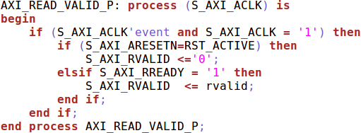
There should be a rule against complicated AXI signaling. Looking over
this user’s custom AXI peripheral, he makes one
of the more fundamental mistakes. RVALID should be set based upon
ARVALID && ARREADY and nothing else! Keep it simple. If your design isn’t
ready to handle the its inputs, then keep ARREADY low. Much to my surprise,
his design was producing two RVALIDs for every ARVALID && ARREADY.
No wonder the design wasn’t working! Had he posted his full custom AXI
module, I would’ve provided a simple formal check–I might’ve even been able
to point out the line that was broken. Indeed, the formal check should’ve
taken place before he ever tried his design in actual hardware. Failing
that, a good firewall
would’ve helped find the problem nicely.
Looking for a tutorial
If the above posts haven’t made the case for it, several users have asked for better training materials. Here’s a user looking for an AXI-lite slave example/tutorial. Here’s another, requesting a custom IP AXI tutorial. Or a third, wondering how to move data from memory to an FPGA processing core and back to memory again. Again, the common theme here is, where shall I go to find the training material I need to learn how to do what I need to?
Not everything fits nicely into official training material. Some questions, like this one on how to handle non-power of two burst lengths, just need simple explanations. Questions like these make the forums fun.
Conclusions
Yes, AXI can be complex. Frankly, it’s becoming the cost of doing business with either a CPU or external memory on an FPGA. Read the specification, study it, and understand it.
You can also look up the various AXI articles I’ve posted. I’ve posted articles on designing both AXI and AXI-lite slaves and masters. We’ve discussed on this blog how to reset AXI designs, and the problems with Xilinx’s DMAs.
Let me also encourage you to formally verify your AXI designs. The formal verification tool can be one of the better teachers you come across. You just need to provide the formal solver with your design and an AXI-lite or AXI property file. Then, run the solver. If the design fails, the solver will give you the line number of a failing property together with a trace showing the bug. Believe me, two hours with a formal solver will fix a lot more bugs in your design than you’ll fix in two hours just trying to get your design placed on hardware.
Finally, let me also point out that a lot of the user problems above could’ve been avoided if the user had access to the RTL designs for the other half of the interface they were working with.
There hath no temptation taken you but such as is common to man: but God is faithful, who will not suffer you to be tempted above that ye are able; but will with the temptation also make a way to escape, that ye may be able to bear it. (1Cor 10:13)