
Putting the pieces together to build a data recorder
Gisselquist Technology, LLC, makes its money primarily off of contract work. I sell occasional licenses to my IP cores, and occasionally teach students, but most of my income is primarily coming from building designs for customers.
How I got to this point as a small businessman is a topic for another day, although one I would very much like to share.
For today, though, I’d like to discuss a project I’ve recently been working on: a basic data recorder.
Well, that’s not quite it. You can purchase data recorders on the market for perhaps cheaper than my hours on this project.
 |
The actual purpose of the project is to design and build a special SONAR communications system and perhaps even a new waveform design to support it, but the first step to getting such a project going is to be able to transmit through a steel medium and then to receive the result on the other side. The focus of this part of the project was on successfully receiving the transmitted waveform.
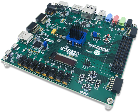 |
Early on, my customer, ExtremeSonar, and I chose a Nexys Video board for the task. Why? First, because I already had the board. Second, because the FPGA on the board was beefy–it’s really overkill for this project. With such a large FPGA I won’t have to worry about running out of logic along the way. Third, we chose this board because it’s an awesome all-around board for a lot of things. In other words, we though that this one board might serve us well for multiple contracts.
Controlling the Transmitter
The first part of the design was to build a transmitter that could select between multiple different waveforms and waveform parameters as we measured how the medium (solid steel) would respond to these various shapes.
We had several waveforms we wanted to try. Building the transmitter was easy, and essentially done in an afternoon.
Then I ran into my first problem: how shall the board be controlled?
 |
The easy answer was to build a design that could be controlled via one or more of the on-board switches. This worked great at the beginning when I wanted to try out four specific waveforms, but each waveform had parameters to it: what modulation should be used? What bit rate should be sent? There were also some hardware specific parameters as well associated with the energy in the transmitted waveform.
It didn’t take long before the sixteen switches on the board just weren’t enough.
My usual approach to solving this problem would be to connect a debugging bus over the serial port and control the waveforms in as much detail as I wanted.
My customer didn’t have access to my debugging bus software, nor did he want that type of low-level access. He wanted a design he could just “plug in” that would then “just work.”
My second approach to this would be to place a ZipCPU on the FPGA so that it could be configured in a more user friendly fashion over a serial port console.
The problem with this approach is that, without the debugging bus, I can’t load flash data into a design. Specifically, I can’t load the ZipCPU’s software on board. Sure, Vivado would load a flash configuration into a design for me–but would Vivado load a ZipCPU program? Yes, I suppose I might’ve bit the bullet and placed a MicroBlaze CPU within the design and done just that. As you’ll see later on in this article, there were good reasons for not doing that.
Instead, I chose to create a ROM memory device on board that would hold the ZipCPU’s software and then control the transmitter from that.
This worked great, and formed the substance of my first delivery. The biggest problem I had with that delivery was that the serial port software my customer was using didn’t support 2MBaud. I suppose this shouldn’t be such a surprise, 2MBaud isn’t really a common rate. I was more surprised to learn that it didn’t support the more common 115.2K Baud either. No, I’d need to run the project at 9600 Baud. Still, for just a basic console, this is plenty fast. For transferring data? Unacceptable, but we haven’t gotten there yet.
Part Two: Receive Data Processing
Building a transmitter is easy. Making it work with a receiver, that’s much harder.
 |
Early on in the project I started building such a receiver, much like the one shown in Fig. 4 on the right. However, when we started questioning how the medium would respond to one data rate vs another, one waveform vs another, etc, I had to abandon those plans. The problem was that I wanted to build a receiver for a waveform of a known symbol type and bit rate, and yet we didn’t yet know if the channel would support either that symbol type and bit rate or not.
We chose instead to record data for offline processing, figuring that if we could demonstrate an offline demodulator for such a data element then it would be easier to place it onto an FPGA.
In hindsight, this should’ve always been my approach from the beginning:
- Build a simulation.
- Demonstrate that the algorithms work in simulation.
- Port the simulation to hardware
 |
Therefore, I scrapped my early receiver drafts and focused instead on getting sampled data I could use to feed such a simulation.
Steel has some very real acoustic properties, and without knowing what those were success might be a challenge. Real data, however, required something I didn’t yet have: a data recorder.
 |
Once I had that data recorder, I could then prove any receiver algorithms and then port the results to hardware.
Today’s story is about building that data recorder.
Building the Data Recorder
Surely a data recorder would be fairly easy: The Nexys Video board has 512MB of SDRAM on it–plenty to stream data into. Indeed, if I streamed data into the board at a maximum speed of 800Mbps (well higher than any desired data rate), there would then be enough room to record over 5s of data before running out of SDRAM. That’s plenty for any need we might have. Not only that, since the Nexys Video board has a micro-SD-Card slot on it, there should be more than enough room on any modern SD-Card to hold any capture I might create.
Ahh, the best laid plans of mice and men.
This was where things started to go wrong.
Sure, I had everything I needed to make this work early on, starting with my own Nexys Video design. This should be easy to modify for a commercial purpose. Indeed, it had already been modified to set up the transmitter.
As built, the design already consisted of several “working” components.
- It had a ZipCPU
- Flash Controller.
- Wishbone to AXI bridge, to control a MIG based DDR3 SDRAM controller
- A serial port based console, with a debugging bus running over the non-printable character set
- I also had a SPI-based SD Card controller to use
- And, of course, the SONAR transmit controller we had used earlier in the project.
This, however, left me missing a couple of key components.
-
I needed a stream to WB recorder. This was an easy build, and took me a quiet and pleasant vacation morning to put together. (Yes, I do enjoy doing this kind of work on my vacations.)
-
AutoFPGA didn’t (yet) handle building projects with multiple masters very well. However, this design required the ability to add more than one bus master (the ZipCPU and the data recorder) to the design. In the end, I chose to upgrade AutoFPGA rather than to manually add another bus arbiter to the design.
The new AutoFPGA upgrade offers the capability to add support for multiple different bus protocols, and multiple bus masters.
This would be the first project to use the updated AutoFPGA support, so there was a bit of risk involved to the project by doing this.
-
I also needed a way to decode the FAT filesystem, and to be able to write a file to the SD-Card using it. After a bit of googling, I found the FATFS project which promised to be able to handle any file system issues for me.
Looking over all of this, most of the work had already been done. I was just adding a couple minor components to the design. What could go wrong?
Everything Fails in Integration
What could go wrong? Everything.
The first problem was that I wanted C-library support to get malloc(),
free(), as well as printf() and its friends. However, the
newlib C-library that I’ve been using
didn’t fit in the 64-kB block RAM image I had allocated for myself in ROM.
Normally this wouldn’t be an issue, as I would’ve just stored any
ZipCPU
software on flash
and then loaded the software from
flash
to SDRAM early on. There was certainly plenty of room on the on-board
flash
chip for any software I might create, so this isn’t (normally) a problem.
 |
My customer, however, didn’t have my debugging tools, nor did he want that kind of access. This left me with no means of getting any software onto the flash memory within his board. (We’re not co-located.) I chose instead to load an SDRAM image from a file on an SD-Card, as shown in Fig. 7 on the left, and then to boot the ZipCPU from that image. This gave me as much code room as I wanted, but required using a special program to load the file into SDRAM–a program that would need to be built into the design itself in a special “Boot ROM” device.
Once this program loaded the ZipCPU’s software into SDRAM, the main program would begin–allowing the user to control waveform types, parameters, and the ability to save files to an SD-Card.
Step One: Gathering Files
The problem with “working designs” is that they change over time. Worse, it had been a long time since I had worked with my “working” Nexys Video design. So, to start this project, I copied all of the files from my “working” Nexys Video design, and then updated them with any changes that had been made since that design.
- The ZipCPU had significantly changed and gotten better. Among other things, it now had a data cache available to me. Even better, since this FPGA had so much logic, there was plenty of room for it as well.
- The flash driver had completely been rewritten.
- The Wishbone to AXI bridge had been completely rewritten, and now enjoyed full formal verification support–something the original driver had never had
- The SDSPI controller, the one that will control an SD-Card. using a SPI based protocol, had been modified to add 75-clocks to it to allow any logic within the SD-Card to start up
- I only really needed to remove the HDMI support that — had never yet worked anyway.
- Also, on my last project, I had updated my favorite debugging bus implementation, fixing some significant bugs in the compression algorithm.
All of this code was easily copied into the new design. It gave me a lot to start from. Even better, all of this code had worked in FPGAs before, so I had a strong confidence that it would work again. Sadly, not all of it had been formally verified. As a result, there were land mines within this design that I was just completely unaware of.
Step One: Simulation
The first step to building something like this was to run the design in simulation and so to demonstrate that it works in simulation alone. To make this happen, I set up two basic simulation setups. The first simulation would run a given program–such as my data collector, and the second simulation would run the boot loader. Selecting between them was as easy as adding a ZipCPU program name to the command line.
From these two, my goal was to demonstrate the ability to boot the ZipCPU from the SD-Card, and then to collect and write/store data to the file system. I would do this first in simulation, then on the actual board.
Connectivity Tests
Normally, I use a small CPU testing program as my way of shaking out a new design. However, as I got to thinking about this, my CPU testing program does nothing to test the rest of the design. Therefore, I chose to create an additional connectivity checking program–one that would attempt to interact with every peripheral within the design and verify that all of the peripherals could be interacted with.
For the most part, this piece of the software worked by 1) reading from some piece of memory, 2) writing a new value to it, 3) verifying that the value was expected, and then 3) returning the value written to its original form. Values chosen included all ones, all zeros, and a variety of patterns in between to make certain all bits could be written and all bytes could be written individually.
I did this because it just felt like “good practice”. It also felt like a complete waste of time, but for the sake of “good practice” I did it anyway.
In hind sight, I’m glad I chose this step. Much to my surprise, there were still bugs in the new AutoFPGA bus logic generation algorithms. This connectivity test helped flush out those bugs during simulation testing. Later on, once everything was passing properly, this connectivity checking program became a confidence builder that my design still worked following any changes.
Indeed, I’m likely to make this kind of connectivity test a standard practice with any new design I build. Having one built now will make building the next one easier.
SD-Card Controller
Now, after all that I’ve learned about digital design, I’m embarrassed to say that my SPI based SD-Card controller was woefully inadequate to the task.
 |
Yes, it had been tested in hardware before. In hardware, I had demonstrated the ability to read a sector, to write all ones or all zeros to the sector, and then to return it to its original value. Sadly, this test was far from automated. As a result, if I didn’t have that original XuLA2-LX25 on my desk (it was in a drawer), nor did I have ISE up and running to build my design, then I couldn’t repeat the test and verify that any changes still worked.
Of course, since using the design in that initial project, the SDSPI controller needed to be modified. Among other things, someone was kind enough to point out to me that the SD-Card protocol requires 75 clocks be sent to the device before any attempt at interacting with it. In it’s previous incarnation, the SD-Card shared SPI pins with the flash chip or I might have noticed this clocking need. However, I dutifully made the change to be compliant with the SD specification.
In the process, I realized that the SPI arbitration code really wasn’t all that relevant anymore. I couldn’t properly remove it, since I have at least one design that uses it, but that didn’t mean I couldn’t parameterize and thus remove the logic for those designs that didn’t need it. Just to make sure I did it right, I started adding formal properties to the lower-level design component where I was making changes.
To make this controller work, I created a low-level software driver with
three basic functions: sdcard_init(), sdcard_read(sector, buffer), and
sdcard_write(sector, buffer). I also created a DiskIO wrapper
for the FATFS library. This then
provided a basic hardware abstraction layer to access the sdcard_* functions.
For simulation work, I had long ago built an SD-Card emulator. To use the emulator, you’d need to create a file on your system which would become the image of the entire SD-Card’s storage. A file system could then be placed onto this image. This made adding a file system to my controller fairly easy to do.
Of course, I expected this to “just work”, right? Since it was “working code” from a prior project (ignore the modifications), it should “just work.”
I was caught by surprise several times during this simulation exercise, however, when code that used to “just work” didn’t “just work” anymore.
First, the FATFS library didn’t
recognize the file system I had on my disk image. I remember just sitting at
my desk, staring at this error, and not knowing where to start to deal
with it. I tried Voodoo logic: changing what wasn’t broken in an effort to fix
what is. It didn’t help. (I appealed to Voodoo logic many more times as the
project went on. While it made me feel like I was doing something productive,
it never really helped.) Eventually, I instrumented the
FATFS library through and through
only to discover when it read the first sector from the
SD-Card,
the controller duplicated the first word and never returned the last word.
Since the last word contained the magic number 16'h55aa, and since
FATFS never found it,
FATFS couldn’t find my
file system.
Of course, since this was in simulation, I was able to quickly chase this down to the controller requiring two clocks to read a value from it’s memory (i.e. the data read from the card), yet the Wishbone ACK was set one clock (not two clocks) after the request. I’d never encountered this bug before, since I’d never read from the controller as fast as my DMA could–I had done most of my testing via my slower Wishbone-over UART debugging bus approach. High speed production reads? Never really tested.
Then, I was caught by surprise again when I discovered that my SD-Card emulator had no write capability. Sure, you could issue write commands successfully, but the emulator never wrote them to the file backed image.
After these many changes, I really wanted to formally verify my SD-Card controller Sadly, the logic was too complex. I couldn’t get induction to pass. Worse, since it since it had been so many years since I had written the design, I struggled to get a grasp on what properties to add.
Nevertheless, I made the changes required and pushed forwards with using this controller–since it had worked in hardware sometime before.
The ZipCPU and the ZipSystem
 |
The ZipSystem is a name I have for an external wrapper to the ZipCPU that contains a set of timers, counters, and possibly even a DMA controller.
Some time back, when doing my crossbar work, I realized that there was a better way to write return decoders that used less logic. Since that time, AutoFPGA’s logic generator has been updated to take advantage of this new method. Seeing that the ZipSystem still used the old method of determining returns, I upgraded that too.
The ZipCPU also had a new hold-in-reset counter. Some FPGAs, notably the iCE40s, require some number of clocks before the block RAMs can be used. While not really needed for this design, this was the last “working” version of the ZipCPU so I copied it into this project. Surely such an extra “feature” wouldn’t hurt, right?
Finally, since I had last worked with my VideoZip example design, I’d built (and formally verified) a data cache for my CPU. Surely this was the time to use it, since I had both a beefy FPGA and room to spare, right?
The first problem with these changes was they broke my ability to simulate a specific software program design. Instead, the simulation would always start at the reset address–regardless of whether or not I told it to start elsewhere.
A quick look into the VCD file generated by the simulation revealed the problem was with the new “hold-in-reset” capability. My top-level simulation script requires the ability to overwrite the CPUs first instruction address, in order to guarantee the CPU starts at the right value–wherever it might be in memory, flash, or SDRAM. However, if the CPU remained in reset, then any time I’d overwrite the value it would get overwritten again with the default reset address before the CPU started.
This was annoying, but certainly fixable.
atoi(“11”)
One of the strangest bugs I came across along the way had to deal with
atoi("11"); returning the wrong value.
This one really threw me for a loop. I couldn’t figure out why the library
code would be broken. I mean, atoi("11") should be pretty basic, right?
The good news with this bug is that the
newlib library I use is fully open
source. That meant that I could modify it if I wanted to. So, I added some
NOUT and NDUMP instructions to announce to the console where it was in the
code, and what various values were along the way. If you don’t remember these
instructions, NOUT
and it’s simulation only SOUT variant can be used to
print characters to the simulation console. NDUMP and SDUMP are similar,
save that they print register values to the console. NSTR is a similar
instruction used to print out strings. For example, NSTR "Hello, World\r\n"
would cause the simulator to print “Hello, World” to the console.
This NSTR “instruction” is actually a pseudo instruction intercepted by the
assembler and then expanded into a sequence of NOUT instructions.
If done right, these instructions won’t modify register assignment at all.
Indeed, I found myself using these options so much I created macros to make placing these instructions into a piece of code even easier:
#define NSTR(A)         asm("NSTR \"" A "\\n\"")
#define NVAL(V)	\
	do {							\
		unsigned tmp = (unsigned)(V);			\
		asm volatile("NDUMP %0":"=r"(tmp):"0"(tmp));	\
	} while(0)
With these modifications, I was able to chase the problem down to two opcodes.
The first bug had to do with the muldi3 GCC opcode. As part of the backend
port, the ZipCPU
needed to implement a muldi3 instruction.
Such an instruction needed to take two ‘di’ (64-bit) values and multiply them
together. Since the ZipCPU only
supports 32x32->64 bit multiplies, the 64x64 bit multiply needed to be converted
into component 32-bit parts, each multiplied separately, and then assembled
back into a 64-bit result.
 |
Doing these component multiplies requires several registers. First, it needs
two registers for each of the incoming operands. Let’s call these H1:L1
and again H2:L2. Further, the way I had written up the algorithm initially,
it also required to scratch registers, S0 and S1 that I could use however
I wanted to. Much to my surprise, however, I found that GCC was only giving
me four registers: the two scratch registers were already H2 and L2!
When I then used these scratch registers mid-algorithm I corrupted the
values I was multiplying.
I rewrote the algorithm here, and so you can see it summarized below. Imagine that H0 and L0 are replaced by one of the operands, and H1 and L1 are replaced by the other. The result is placed into H0:L0.
	MOV	L1,L0
	MPY	L1,L0	;	L0 = L1^2
	MOV	H1,H0
	MPY	L1,H0	;	H0 = L1 * H1
	LSL	1,H0	;	H0 = (L1 * H1)*2
	MPYUHI	L1,L1
	ADD	L1,H0
(GCC actually requires a % before each of these place-holder register
names.)
Yes, I do put comments into my GCC generated assembly. It really helps debug the assembly later when you start trying to figure out what GCC was doing.
The second bug was an unsigned A >= B comparison. Since the
ZipCPU
didn’t initially support unsigned A >= B comparisons, the GCC backend needed
to silently convert these into “equivalent” A +1 > B comparisons which the
ZipCPU supported. The problem, however,
is that if A is the maximum positive value, then
(Maximum positive value) >= B doesn’t have the same meaning as 0 > B,
where 0 is the (Maximum positive value) plus one.
One of the failings of my current GCC backend is that I’m not using any of GCC’s regression test suite. This was originally due to the fact that the ZipCPU didn’t have C-library support due to a lack of 8-bit byte support. (The ZipCPU originally supported only 32-bit bytes.) Now that the ZipCPU supports the full C-library via Newlib, I really should go back and enable the automated testing to find problems like this earlier.
One of the other “bugs” I finally dealt with in this design was a frustration
I’ve often had with the SIM instructions. SIM instructions are what I refer
to the class of instructions just for the simulator, containing the NOUT
and NDUMP instructions I was using among other things. Because of how they
were implemented, before any conditional checks, it was possible that a prior
branch instruction would execute and then the SIM instruction would execute
anyway.
For example, in the following code, R1 should only be printed if the Z
(zero) condition code isn’t set.
	BZ	_some_target
	NDUMP	R1
The problem was that these special SIM instructions were getting retired
prior to the last pipeline stage, and might possibly get eliminated by a
jump at the last stage.
This time, I finally got fed up with the bug enough to fix it. (The fix
hasn’t been backported yet …) I pushed the SIM instruction information
into the ALU pipeline stage, not just the read-operand stage, and so hopefully
I’ve fixed this for all time–or at least until I try running my next design.
Stream Recorder
The stream recorder used by this project was a new core of mine. It wasn’t all that hard to create, and I managed to verify it and build it within about 6 hrs of work or so. In many ways, it’s very similar to my AXI stream to memory bridge–although that one took closer to 20hrs of work to build and verify.
Time is money, right? See why I like Wishbone? It’s so much easier to work with.
 |
After building this stream processing core, I decided that I really wanted a high speed access to my SDRAM device. Therefore, I connected this to a 128-bit Wishbone bus that contained only the SDRAM memory slave as shown in Fig. 11 on the left. Normally, I just use 32-bit Wishbone buses for everything, but if I wanted to record 800Mbps of data–why not use the full memory data rate?
With the new AutoFPGA updates, AutoFPGA could now handle creating a special 128-bit bus with two masters on it–my normal 32-bit bus with a bus-expander on it, and the stream recorder.
Of course, this meant that my memory emulator needed updates as well, since most desktops can’t handle 128-bit words natively.
 |
My design then worked perfectly! Perfectly, that is, until I tried to use the
recorder. As it turns out, I had forgotten that the Stream to WB capability
required an aligned address, and connecting it to a 128-bit bus meant that
it now needed a 128-bit aligned address. Malloc only generated a word-aligned
(i.e. 32-bit aligned) addresses for me. If I then used the recorder with this
not-quite-aligned address, it would overwrite the malloc
data structure, as shown in Fig. 12, and then the
CPU
would crash when I tried to free() the memory later.
Ouch!
Again, think of where you’d look for this bug: In the new Stream2WB core? Or
in the free() library call that failed with the
bus
error?
It’s easy to write about these bugs today, long after they were found, but finding where to look for them in the first place was a real challenge–especially given that I was under a lot of schedule pressure.
In my case, that meant generating a
VCD trace
starting from CPU startup through stream to memory data write and the following
memory free() where the CPU would stop on a
bus
error.
I could then read off the instruction pointer from the CPU
trace,
but it pointed to
newlib library code that, when I stared at
the disassembly of, I wasn’t familiar with. When I examined the
newlib code responsible, I couldn’t
see any bugs–so what happened to this memory value? When did it get changed?
To find this, I adjusted my test-bench wrapper to check that memory address and report any changes to it. I could then see the address given the “right” value, and then get overwritten with the wrong value. The time-stamp of this change pointed me to time in the VCD trace when the recorder just started recording–and then I had one of those forehead smacking moments, when I realized the core was doing just what I had designed it to do but that since designing it to do that I had forgotten about the reality that it didn’t support unaligned transfers.
Step Two: Hardware
That was a lot of bugs to find in “working” code! I’m thankful that I was able to find those in simulation. I’m not sure how I would’ve found all of those in actual hardware. The result, however, was that the design now worked in simulation, and so it was time to move to hardware.
I suppose I should’ve been excited at the prospect of moving to hardware. I wasn’t. I’m often reluctant to leave simulation, simply because once the design “works” in simulation it then “works”, right? Only two things can happen in hardware. Either it continues to “just work” (not likely), or the harder hardware debugging starts.
I had no choice, I was getting paid, so I bit the bullet and started my design in hardware–but not after enjoying a quiet weekend, Friday night movie, etc. I certainly needed a break to celebrate my “success” while it lasted.
When I then ran the design in hardware, it crashed so hard I thought the power got pulled somehow. My serial port to TCP/IP converter suddenly closed due to an underlying error, the telnet I was using for my console port closed, and … what just happened?
Sigh.
Time to start debugging.
FIFO bugs
The only clue I had to what was going wrong was that there was a “bus error” in the debugging bus. Sadly, that doesn’t help me much. My best guess was that the FIFO I was using was somehow flawed. Perhaps it was overflowing or reading the wrong value? So I tore it apart and added formal properties to it. Sure enough, I found bugs within it. Those were easy to clean up, though. Verifying FIFOs is fairly basic–although my most recent article on the topic is woefully out of date–I’ve just learned so much since writing it. (The tutorial lesson is pretty good, though.)
I then ran the CPU’s self-test, and then my new connectivity test. When the results didn’t look right, I placed a Wishbone Scope onto the console port. Sure enough, I wasn’t reading the right values from the console. That meant my UART FIFO was broken as well.
Yes, this was frustrating to me. I’d just found bugs in two FIFOs I’d had and used in many different projects over the course of several years. No, neither of these cores had been formally verified. No more, though. Now they were verified, the bugs were gone, I could prove that they were gone, and I could now move on.
[Eric Brombaugh]’s response to my tweet about this really captured my own thoughts:
 |
I’m truly hoping this happens soon.
Of course, even after fixing these two FIFOs I still knew that I had more bugs in this design–I just didn’t know where. For example, I still hadn’t found that power supply issue I started out with. Therefore, since I knew I was going to need to do some serious work, I upped the speed of the debugging bus back up from 9.6KBaud on up to 2MBaud again.
The next bug took place in software, so I then turned to my Wishbone Scope attached to the ZipCPU. When the results didn’t make sense, I dug in further and discovered the CPU was trying to execute the wrong instruction at one point. Where was it getting the wrong instruction from? I started attaching WBScopes further and further up stream towards the memory.
Sure enough, I saw the wrong instruction come back from my bus expander.
Let me back up to explain this one, though. The bus expander takes a Wishbone request at one data width, and converts it to a request at another data width that’s larger than the first. In this case, it converts a 32-bit request to a 128-bit request, as shown in Fig. 11 above. To make this work, the lower bits of the address, the bits that aren’t needed on the 128-bit bus, are recorded in a FIFO. Then, when the 128-bit word is read, the 32-bit value of interest is selected from that 128-bit value using those lower address bits.
Did you catch the word FIFO in that paragraph?
Sure enough, this “hardware-proven” bus expander, the one I’d used on my VideoZip project years earlier, had no FIFO overflow checking! How on earth had it ever worked earlier? I must’ve never made more than 16 requests (the size of the FIFO), and so it would’ve never overran before. This time, however, I had the instruction cache line size configured to 64-words. Even at that, it almost worked: the FIFO almost overflowed and then recovered since the data within it was essentially a counter. (The cache was reading words in order, after all.) What kept it from working now was that my new crossbar interconnect required one extra clock stall cycle to get through the arbiter. This stall caused the first value to stall and hence write the same bottom address bits to the expander twice.
Ouch. Burned again by “working in FPGA” qualified code, but not “formally verified” code. You’d think I’d learn by now, no?
Okay, well I’d now found a lot of bugs. Surely the design would work by now, right?
Xilinx’s MIG: It’s not my fault! (when it was)
It still didn’t work.
Again, I chased down the bugs I could as best I could. As before, I’d find the symptom of something that was broken, and then attach WBScopes further and further upstream until I found the cause.
Much to my surprise, I found an AXI error when working with Xilinx’s MIG controller.
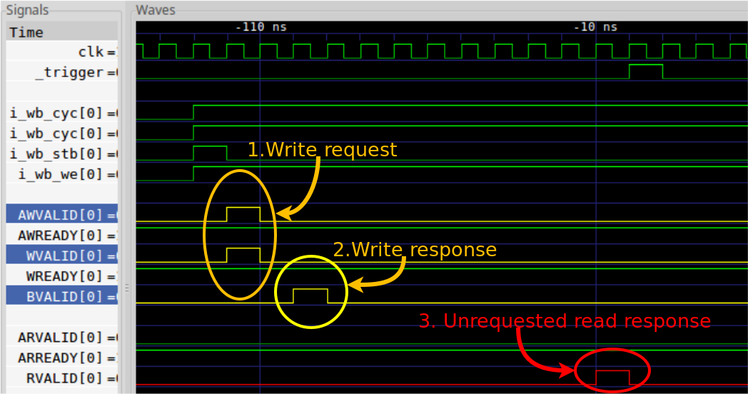 |
How on earth would a write request return an unrequested read response? This made no sense.
So, I contacted Xilinx. You can read my description of the bug here, although Xilinx’s representative and I went back and forth over this several times off-forum.
I was convinced the bug was in their code. The component of mine that interacted with their controller had been fully and formally verified. Further, I counted requests internal to that controller, and examining that request count I could see that this wasn’t a response to any outstanding requests.
Xilinx’s tech support, however, was just as confused by the trace as I was. Perhaps there was a read request from earlier that hadn’t been returned? So … I traced four seconds of return, and proved that every prior read request had been properly returned. (At the time, I didn’t realize just how truly awesome the compressed version of the Wishbone scope really was …) Perhaps a request of mine broke protocol and crossed a 4kB boundary? Couldn’t happen, I said, since none of my requests were ever for more than a single beat.
When they pointed out to me that it was unlikely their code had such an egregious bug in it after so many others had used it, I quietly had to agree. Surely even I would’ve seen this bug before if it was in their basic AXI handling?
Sadly, that also meant that I was really on my own to find the bug. Well, that and the fact that I was the only one with a design that had symptoms of being “broken”. (I didn’t want to give my design away by posting it on the forum …)
With a little bit of digging, I discovered how to open a design after Synthesis. I learned how to use Xilinx’s Internal Logic Analyzer. (Yes, this was my first WBScope time–I’ve only ever used my own Wishbone scope before.) I then tore into the MIG controller looking for where this extraneous return came from.
No, I never found any similar compression capability in the ILA.
 |
The AXI_RVALID signal came from a hardware FIFO, leading to a design FIFO,
leading to the AXI_RVALID line shown in the trace above. The only way this
hardware FIFO would return an invalid value would be if the memory returned a
read response–one that I hadn’t requested.
Hmm …
The other unusual thing about this bug was that there was always activity on the “user interface” to the memory taking place at the same time. It wasn’t my activity. I was using the AXI interface. Internally, the MIG controller turns the AXI interface into a “user interface” internally, then drives a “native interface” from this “user interface”, and from that drives the memory itself. This extra activity on the “user interface” was in addition to the activity my own code was causing.
At this point I remembered hearing, some time ago, that Xilinx’s MIG controller needed to read from the memory periodically just to keep it’s PLL’s locked. That made sense of the extra activity, but this activity should’ve never produced a response. Surely their MIG controller was designed to suppress this return, so why would I see it?
I stared at this bug for a week.
That’s a week I didn’t have for this project. The project was already due. Indeed, it was past due. I hadn’t scheduled this time. I was only going to be updating an already working “FPGA proven” design. How could I be struggling with a bug this fundamental?
I tried blaming others. No one else was able to help without being able to reproduce the bug, for which they’d need my design and my hardware.
I tried taking the dog for a walk, hoping something would come to me.
Nope, nothing.
I considered using the litedram controller, and then gave up when I realized how much setup would be required.
Surely there was an easier way to fix this memory bug than learning how to integrate with a new language, no?
Let me at least say this: When all else fails, prayer still works.
No, I don’t have control over God. No, He’s not required to help me any time I want. That said, He enjoys helping me.
For the eyes of the LORD run to and fro throughout the whole earth, to shew Himself strong in the behalf of them whose heart is perfect toward Him. … (2 Chron 16:9a)
He also likes waiting for me to humbly come to Him, which tends not to happen until after I’ve exhausted every option. At that point, the point when there’s no other option, and no where else help might come from, I turn to seriously begging.
It’s quite humbling.
Humble yourselves in the sight of the Lord, and he shall lift you up. (James 4:10)
I certainly didn’t know where else to look, and the schedule stress wasn’t helping.
Sometime after praying (more than once, I might add), I got the idea to check the memory chip set up against the schematic. Sure enough, I had configured the MIG for the wrong memory chip.
This also explains the bug. The MIG controller was expecting a response from the memory chip a certain number of clocks after its request, and due to the misconfiguration it suppressed the response from the wrong clock window.
No, it wasn’t Xilinx’s fault. In spite of all my rants and frustrations, it was my own code at fault. (I’m sorry, Xilinx employees, wherever and whoever you are, for ever speaking poorly about your controller and swearing it didn’t work. It was my fault all the time. This time …)
Time to take a break, and then try again. Surely the design will now work, right? I mean, I started with a “working” design, many of the parts and pieces had been either formally verified or FPGA proven before I started working with them, what more could go wrong?
Data Cache Bugs
There were still two problems with the ZipCPU that I didn’t catch until moving to hardware. Both of these were related to the ZipCPU’s bootloader.
The first problem was annoying, although I’d seen it before.
In my linker scripts, I define a set of values indicating which pieces of ROM (flash, boot ROM), kernel RAM (block RAM only) or RAM (block RAM or SDRAM) are on board. These addresses are provided by AutoFPGA when the design is put together, and may change as components are added or removed from the design.
To capture these values into my program, I use statements such as,
extern unsigned _rom[1];References to _rom now become pointer references, filled in by the
linker–just what I want. Other approaches, such as declaring an external
unsigned pointer _rom, tended to create memory allocations for the pointer.
This method of declaration simply evaluates to the right answer when
I want it.
The problem comes about when my boot loader software checks to see if there’s a ROM image to copy from.
bootloader(...) {
	// ...
	if (_rom != NULL) {
		// We need to copy the ROM image to RAM
	}
	//
	// Other code
}
The problem with this code is that the GCC compiler “knows” that _rom isn’t
a NULL pointer, it’s a pointer to a properly allocated memory array. (When it
might actually be a NULL pointer …) As a result, this check gets dropped from
the code.
So, I replaced the check with something that looked like,
#define NOTNULL (4 != (unsigned)&A[1])and then later,
	if (NOTNULL(_rom)) {
		// ...
	}
While I’m sure there’s a better way, this worked and by now I was both behind and frustrated.
The next bug I should’ve anticipated as well. I was copying from the ROM memory image of my code into RAM (i.e. setting global values), yet also using that same RAM for some debugging statements.
I know, I shouldn’t do that. But the problem wasn’t severe–I just wanted to print out certain values, and my print routine wanted to use a global to know if the last character printed was a carriage return or not. If it was a carriage return, it would send a new-line and suppress the next newline. This effectively turned a “\r\n” sequence into a “\n” sequence.
If the “last-character-was-a-newline” value was wrong, the result wouldn’t look pretty but it would still work.
In this case, the bug I was getting was worse. There was another global value that wasn’t getting set properly.
As with the other hardware bugs, I attached a Wishbone Scope and started digging. I should mention, this type of digging is a slow process. It took Vivado about 15 minutes to create a bit file following any changes. I’d then run the design, examine the trace, adjust things and try again. This kind of debugging loop is quite slow. Eventually, though, I tend to try running the simulator to see if the same bug pops up since chasing a bug through a simulation trace is a whole lot easier than moving a Wishbone Scope around and rebuilding again.
 |
When I finally got to the root of the issue, I could’ve kicked myself. Using the value from the RAM that hadn’t yet been initialized caused that uninitialized cache line (not just the one uninitialized value) to get loaded into the data cache. The bootloader would then copy data from the ROM image to the RAM area where the globals would be stored using the DMA. The data cache, however, was unaware of the DMA’s accesses, and so the cache is now out of sync with memory–as shown in Fig. 15 on the right.
Once I realized what was causing the bug, fixing it was easy: I expanded my “clear cache” instruction to work on the data cache, as well as the more established instruction cache.
SDSPI: The I/O Drivers
The big risk in this project, of course, was using the SD-Card.
I knew it was a risk because I had never used the FATFS library before.
Note that I didn’t consider the fact that I’d never used the SD-Card on this hardware before a risk, nor did I consider using my SD Card controller a risk since it had “worked” when it was last used.
I tried the design first without an SD-Card in place.
I quickly realized that I needed to adjust my controller to detect whether or not the card was present. Digilent’s Nexys Video board also includes an electronic reset to the card that pulls power from it. I adjusted my controller again, so that this reset signal would release the controller from whatever action it was in the middle of if the reset signal were present.
To understand what happened next, you need to understand the first step in any
SD-Card
interaction over SPI. The software driver needs to send the
SD-Card
a reset command, commonly called a “SEND_GO_IDLE” or CMD0 command. The
card then responds with an R1 response as it’s called–basically an 8-bit
value equal to 8'h01.
My controller sent this CMD0 and got no response.
Now what?
It had been years since I’d worked with this controller. Sadly, I didn’t remember much of how it worked. I wasn’t certain where to start debugging. Still, it had a debugging output which I could place into a WBScope again.
I saw 7 good clock pulses per byte, and one strangely short one.
 |
I quickly modified the lower-level driver to fix it.
I then saw the outgoing MOSI line change while SCK was high.
 |
No, this isn’t allowed–not on one of my cores. I wanted the MOSI line to
only change when SCK fell–never otherwise. So I tore the lower level
driver apart.
This time I rewrote it. I added formal properties to it. I verified the
interface against something similar to an AXI stream protocol. (I used
STB and IDLE instead of VALID and READY …) I ran cover() checks.
It now worked exactly as desired and designed, so I tried again.
Still no response from the SD-Card.
Not again.
I reread the SD specification I had. I double checked the power up sequencing. No, this was right. Just for good measure, I stuffed a 1ms power-up delay into the lower level controller and tried again. Still nothing.
This time I turned to Google. I started getting worried that my off-the-shelf SD-Cards didn’t support SPI. I was using both SanDisk and Lexar cards, and with a bit of Googling I found the specification sheet for another similar SanDisk card. While it wasn’t quite the specification for my card, it did verify that SanDisk supported SPI mode on at least one SD-Card. It also verified how the timing was supposed to work.
No, this should work.
So, for the first time, I went and checked Vivado’s warnings. Sure enough, I had warnings for the following four lines:
	assign	io_sd[0] = w_sd[0] ? 1'bz : 0
	assign	io_sd[1] = w_sd[1] ? 1'bz : 0
	assign	io_sd[2] = w_sd[2] ? 1'bz : 0
	assign	io_sd[3] = w_sd[3] ? 1'bz : 0
These four lines are used to set the I/O lines to 1’b1 (via an external pullup) or 1’b0 if the I/O is active. They are really only important when implementing the full SDIO interface, but that’s what Digilent had wired and so it was what I was using here.
Since Vivado had a problem with these lines, I replaced them with IOBUF
instantiations that should’ve done the same thing. I then convinced myself
of a bug in these instantiations, changed them, and changed them again, until
I finally had no confidence at all in my IOBUF instantiations.
With no other way to debug these, I stuffed the return values of the IOBUFs
into a
WBScope.
Much to my surprise, even though the outgoing data wires
were toggling appropriately, the IOBUF return values didn’t reflect that at
all.
So I got rid of the 1'bz values entirely. I suppose it’s not really a big
deal. While the SDIO protocol uses them the SPI protocol doesn’t, so I
figured I should still be good.
Suddenly, and much to my delight, the card I was working with responded!
 |
Surly my adventure was coming to an end, right?
SDSPI: The Jenga Design
Sadly, no. This “adventure” was far from complete. Worse, I was now nearly two weeks later than I wanted to be in my project schedule. At least I had the SDSPI controller fully connected to the WBScope so I could see what was going on.
Before going further, let me share some more about this design. I wrote this design as one of my earlier digital design projects–back when I was still “thinking like a programmer” if you will. As a result the state machine within it was incredibly complex–too complex even. Indeed, it was so complex that ISE wouldn’t even place a design with this controller in it without failing timing.
Timing shouldn’t be a problem for a SPI transaction, right?
I had eventually “fixed” the problem years ago by (slightly) breaking up the giant always block so that smaller blocks would pre-calculate values. I also removed any extraneous logic.
 |
The result was what I’m going to call a “Jenga” design, after the classic game from Hasbro. That game starts with a wooden tower, from which players one by one remove support elements and place them on top. When the tower finally falls (which it will do), the last person to remove a support loses.
Why was this a “Jenga” design? Well, obviously, because it appeared to be designed to fail. (Yes, this was one of my own designs …) First, it was so badly written I couldn’t tell from reading my own code how it was supposed to work. That meant that, second, I couldn’t track the dependencies through the design–what signals were dependent upon which others? Worse, when I just slightly modified the lower-level I/O controller, the data out valid line was delayed by one clock from the data in valid line and … this was causing my whole design to fail. The Jenga design had been changed just one too many times.
I tried patching it. The patch fixed one problem, but generated another.
No matter how I looked at it, there was just no easy way to fix it–especially without a good understanding of how it was supposed to work originally.
The project was already late, now what?
Seeing no other way forward, I tore the entire design apart and rebuilt it using formal verification properties from the ground up. In about a day I had a newer design with much simpler state machines. Even better, the newer design was separated into three new but separate modules: sending a command, receiving a buffer of data, and sending a buffer of data to the SD-Card. The lower level controller remained the same, but I could now gut most of the Jenga design and in particular I was able to remove the unmaintainable state machine and replace it with something much simpler.
Not only that, but I could use the formal tools to generate waveforms illustrating how each component was supposed to work. Not only that, I could formally verify the whole using induction–something I could never do with the previous Jenga design.
Now, finally, perhaps the design would work?
Not quite. The first step as always was simulation.
In simulation, I discovered that the CRC generation and checking code for the data blocks wasn’t working. (The one part I didn’t formally verify in my haste …)
Still, I was in a hurry. After some quick changes, my design worked in simulation, I moved to hardware.
SD-Cards, and an Undocumented Feature
I’m now just over two weeks late. Does this design work now?
Sadly, no.
After running my design, something went wrong. Badly wrong. I started getting file system not found errors. Resetting the card and reading the (hopefully constant) CSD register returned values completely unexpected.
Ouch.
I reformatted the card, placed my software image on it and tried again.
Again, something, somehow, somewhere again went badly wrong.
I adjusted the software so that any block read or write would dump to the screen. I captured the screen using script. I scrolled back and examined what was going on.
 |
Needless to say, I started staring at pages and pages of tables looking sort of like Fig. 20 on the right.
Out of luck, I happened to notice a dumped data block showing a write to the
file system that looked more
like Fig. 21 below than the prior read that had looked like Fig. 20 above.
(Colors added for effect, since no one reading will want to stare at hex
values.) I started to look deeper. Sure enough, it lead to finding a bug
in the new (hastily-verified) controller.
 |
This bug was easy to chase down. My new data-write module needed to read from a (block RAM) memory external to it, and grabbed the value one clock too late–after the new address changed the value. Getting this timing right was one of those things I hadn’t checked in my haste.
I adjusted the timing and tried again.
Nope, still not working. In particular, the SD-Card was returning error responses. Perhaps I could chase those down?
So I turned to the WBScope again to see what was going on. This time, I triggered the scope off of the first operation that received a failing return from the card and … saw something I wasn’t expecting at all.
The card was returning multiple acknowledgements even while a block was being written.
This was … unexpected. It was as though the card were responding to the data I was transmitting as though they were commands and not data.
I adjusted the scope’s trigger and tried again, hoping to get a better look.
At one point, I increased the memory in the scope and even adjusted its trigger in logic. I reformatted my (now long-since broken) SD-Card, put my application’s image on it again and loaded my design (again).
Much to my surprise, I watched the boot loader properly set up the card, read my design into SDRAM, and then start and run the design.
This shocked me. I thought I was suffering from bugs still. How did this much logic manage to work without error? Indeed, everything worked well until the design then tried to write to the SD-Card.
Somewhere around this time, things started to add up.
SD-Cards have some work to do following a write. If you send the card enough writes, back to back, you need to expect that the card will ask you to slow down. Forget the data rates quoted on the manufacturers sites. Cards are slower than that, they just transfer at that rate.
So I checked the SD Spec again.
Sure enough, there was a means of signaling that the card isn’t ready–by holding D0 low following a command in SDIO mode. Nothing was said about this, however, in SPI mode.
Perhaps this was an oversight?
So I went back to my new SDSPI controller and adjusted the write-data command
so that it would wait until the card was idle (i.e. MISO returned an 8'hff
instead of an 8'h00).
Finally, after all this work, the design works from bring up through a data record and write to the SD-Card.
Whew!
The “Power” Failure
What about that initial bug? You know, the one that looked like a power failure?
At this point, I was declaring success yet I had never seen that power bug since I first started working in actual hardware. Indeed, I’d almost forgotten about it.
Still, I was running my serial port at 2MBaud–a rate that wouldn’t work when I delivered this code. So I switched back to 9.6KBaud to meet my customer’s requirement.
Just to run a final test, I ran my design at 9.6kBaud. This time, however, when I tried to load it into memory the loader shut down and the UART to TCP/IP bridge suddenly quit again as well.
This looked like that ugly “power” problem rearing it’s head again.
Sigh. Just when I thought things were working.
This time, however, I knew things were working before changing serial port speed. Could it be something speed related?
Sure enough, after describing the problem to my family, I remembered a timer within the debugging bus I’d built. Specifically, there’s a watchdog timer within it. The purpose of the timer is to keep the Wishbone bus from ever locking up. The timer starts when the bus is activated, and clears when either the bus becomes idle or a new request is accepted. This timer is set to count a rough 500M clocks. If the bus isn’t released in 500M clocks, the debugging bus will return bus error.
To understand more of what’s going on, know that this version of the debugging
bus
takes at least 6-bytes to transmit a 32-bit word. At 100MHz and 9600Baud,
one baud clock will require about 10.5k clocks. Ten baud clocks constitute
one character, and six characters are needed for a total of about 625,000
clocks. Further, in order to support my original flash
driver,
the debugging bus
doesn’t release the CYC line following any write until the whole
pattern is written. Hence the first write goes through fine, and the bus is
held for the second write. It then takes 625k clocks to get the second piece
of data, during which time the watchdog times out and the debugging bus
returns a bus
error.
That bus error then gets returned to the ZipCPU loader. This is turned into an C++ exception within the loader. When the loader then receives this exception, it suddenly exits complaining about a bus error. Worse, since it exits mid TCP/IP connection, the TCP/IP connection is suddenly reset which then creates an error in the TCP/IP bridge–leaving me believing a “power failure” had taken place that caused me to lose my connection to the FTDI chip.
Conclusion
Wait, what just happened?
What happened was that I didn’t allocate enough time to get a “working”, “FPGA proven” design to work.
What happened was that I lost more than two weeks of schedule on an already late project.
Did formal verification help? Most certainly! Notice that every one of the FIFOs within my design that wasn’t formally verified had bugs in it. Notice also how I was able to build a brand new SDSPI controller, using formal tools, in just over a day. Notice also how it was possible to quickly adjust that controller to meet the “undocumented feature” in the SD-Card protocol.
That said, I wouldn’t have been able to do any of this without my WBScope. I can also finally describe how it’s different from Xilinx’s Internal Logic Analyzer.
First, I give Xilinx full marks for their ability to integrate their Internal Logic Analyzer into their Vivado design flow. Using Vivado, I found it possible to trace lines within code that I didn’t feel like I could change. After selecting the lines I was interested in, there was little more required to set it up. Again, full marks for simplicity in set up.
That said, the WBScope has some capabilities that I didn’t find with Xilinx’s ILA. The first major difference is that I have a compressed version of the Wishbone scope. The compression itself is really quite simple–it’s just a basic run-length encoder. Still, that simple compression was enough to examine every transaction from startup to some time between 4-13 seconds later. The second major difference is that the WBScope can be either 1) externally triggered, triggered from an internal hardware event, or even 2) triggered internally from software. Given that software changes took a rough 30s to modify, triggering from software was much faster than rebuilding the design to look for a new trigger. It also allowed me to trigger off of some rather strange trigger conditions.
Finally, I am also very thankful that, when the chips were down, God answered my prayers.
Thank you, Lord.
Ask, and it shall be given you; seek, and ye shall find; knock, and it shall be opened unto you (Matt 7:7)