
Four keys to getting your design to work the first time
 |
When I first started working with formal verification, I was used to chasing bugs in FPGA hardware implementations. While difficult, I figured this was just how things worked.
Now, after working with SymbiYosys since 2017, I’ve gotten to the point where I’ve now had several designs work the very first time they were tried in actual FPGA hardware.
One of the first examples of such a design was my AXI-lite slave. I offered it as an example to someone who was struggling to make Xilinx’s example work, and mine “just worked” for him. No, I never told him that it had never before been tried in real hardware, nor that it had never before been tried with Vivado, still it “just worked.”
 |
Then, about three weeks ago, I learned of another example. [RLEE287] was struggling with what turned out to be an unexpected “feature” of Xilinx’s AXIS2MM core, and so he had taken my AXIMM2S and AXIS2MM designs and incorporated them into his own work. He then placed the designs within an FPGA, and sure enough my two components “just worked.”
Now, here’s the hidden secret behind that test: I’d never tried these even more complicated designs in hardware before either. Nope, not at all. The only thing I’d done was to formally verify the design. (Well, okay, that and a little bit of a simulation check–which both cores had previously passed.)
Indeed, I’m now spending a lot less time chasing bugs in hardware than I ever was before. Unlike before, where I was used to struggling to find a broken needle in a haystack of traces using a straw called an internal logic analyzer for glasses, I’m now fixing bugs found by a tool that tells me exactly where the bug is and gives me a very short trace illustrating the bug. Needless to say, bug hunting has gotten a lot easier.
Four Keys to getting a design that “Just Works”
If I were to try to turn this into a formula for success, I’d argue that there are four key components common to each of these successes, as illustrated in Fig. 1 above: A formal contract, interface property sets, functional coverage checking, and induction. Let’s discuss each of these briefly in turn.
 |
-
The Formal “Contract”
A common thread among all of my “successful first time” components is that they have all been verified against a formal “contract”. This “contract” is unique to each component, and follows an application (not component) specific form. The contract fundamentally describes the underlying nature of the component. For example, when writing data to a memory, there should be a series of formal properties describing the logic path from the bus to the memory and back again. When verifying a flash controller, there should be a property expressing every step involved in reading from the flash all the way up to the bus return. When verifying a CPU, the contract should follow an instruction through the pipeline and verify that the “right thing” happens at every step. The “contract” is really a fundamental part of any formal proof.
-
Interface Property Sets
All interfaces between internal design components should be verified against an interface property set. This is perhaps most pronounced with bus interfaces, but it applies to other interfaces as well.
 |
Before I started formally verifying my designs, it wasn’t uncommon to have a design that somehow dropped a bus request that would then hang the whole bus. This is one of the reasons why I really like Wishbone’s ability to “abort” a bus cycle–a feature not present in AXI. I would then attempt to recover the design by aborting the broken cycle (dropping the CYC line before the last ACK). Once aborted, I could then return to the bus and read from my Wishbone Scope to find out what had happened. Without the abort, I wouldn’t have been able to access the WB scope at all following a bus fault.
Since I’ve started formally verifying all of my bus component designs, I’ve stopped needing to abort transactions in order to rescue a bus. I’m simply just not struggling with bus faults like this anymore. Well, there was an exception at one time due to a fault in the interconnect, dating back to before I formally verified my interconnect. There was also another exception due to a faulty bus property set, but these tend to be the rare exceptions rather than the rule.
Let me also add another lesson learned here from building the ZipCPU. In every instruction fetch component, and in every data memory component, I found myself duplicating interface properties describing the interface between the CPU and the respective memory controller. This left me with the hassle of visually inspecting each property within the memory controllers to make sure there was a corresponding one within the CPU, as well as struggling with version controlling these properties since I had so many copies of them across the design. Had I instead just created a single custom formal property set to describe the instruction fetch interface, and another one for the data memory controller, managing the properties would’ve been so much easier.
My point? Interface property sets are awesome! They make an easy addition to any project, and they can really help isolate and abstract components that should be working together.
-
Functional coverage
My third rule is that you need to be able to
cover()every possible operation the component is supposed to accomplish. This helps to flush out careless assumptions that might otherwise prevent the proof from being valid.
 |
As examples, a
flash controller,
should be able to request a value from the device and return the response.
It should be able to request a second value, in quick succession and return
that too. In both cases, you want to cover() the return of the design
back to idle.
Likewise, a CPU cache should be able to make a memory request, get the result, and return it to the CPU–with appropriate assertion checking along the way of course. The CPU itself should be able to retire instructions of each basic category. Cover requests should include requests for items in the cache as well as items not in the cache. They should include requests for cachable memory, as well as I/O memory–as well as multiple requests in short succession.
An SDRAM component should be able to properly reset the device, activate a row, and then read or write from a column of memory. It should even be able to activate a second row and read or write from that row while working with the first. My own cover checks go farther to check that, after working with one row, the memory should be able to switch rows or even issue a refresh command.
The fun part of this functional coverage check is that the result is a trace
showing how well the core works. Usually I’ll just cover the 3rd or 4th
return from a bus slave, which then reveals the throughput of the core.
I’ve since used these traces often when advertising the operation of the
core. I’ve used them when explaining to users how the core works. Indeed,
if you check the
doc/gfx
directories of some of my repositories, you are likely to find the results
of any cover checks of more recent cores. Here, for example, is a
trace
drawn from my AXIDMA
core
showing it’s ability to maintain 100% AXI throughput even when crossing
burst boundaries.
When should cover be checked? Some engineers check it early in the verification process. While I’ve done that, my focus on cover checks is typically the last step in the process–something that makes the cover check feel like the icing on the cake of a new design. This “icing” helps to prove that, not only does the design not violate any interface rules, but also that it has been well designed.
 |
-
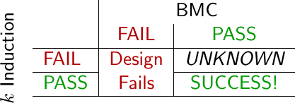
Induction
The fourth ingredient that has been common among my “successes” is that I insist that all my designs must pass an induction check. A bounded model check (BMC) will only ever prove that your design can handle some number of initial clock cycles without any error. The induction check, if passed, will additionally prove that your design will never violate any properties within the design. Never.
 |
This proof is subject, of course, to the hardware implementing your logic properly but that’s really another story. For this reason, we’ll avoid any discussion here of the very real problems asssociated with manufacturing flaws, power dropouts, PLLs that don’t lock properly, or the unique problems associated with extra-terrestrial environments. Barring such faults, a design passing an induction check will never violate any of your safety properties (i.e. your assertions) for all time.
When starting out with a new design, I try to start out with a proof length equal to or greater than the length of a core operation–whatever that is for the particular design at hand. Sometimes I can start with two operations, although it really depends upon the core. Not every design can fit in this mold. AXI bursts, for example, can be up to 256 beats in length, and checking back pressure can require a many more steps than that. AXI is a complicated protocol, however, and so I struggle to complete a proof much longer than 50 steps or so. Sometimes even 10 steps is too hard. As a result, few of my AXI proofs are longer than 20 steps, and the more complex proofs are even smaller. For example, my AXI crossbar proof only requires 5 steps, whereas the AXI DMA proof requires only 3 steps. Short but complete proofs like this are only possible when using induction.
What sorts of problems get caught with induction checks? The big things seem to be counter or buffer overflows, but the list could go on quite a ways. For example, any crossbar needs to keep track of the number of outstanding transactions so that it can know when to adjust it’s arbitration rules. What will verify the logic required to keep this counter from overflowing? That’s something that you can typically only check using induction.
 |
At the same time, I’ll admit that induction checks offer diminishing returns. Towards the end of any project, most of the induction faults will be caused by missing assertions rather than broken logic. Still, until the design passes an inductive check, you don’t have any confidence of anything truly “working”, and a design that “just works” when it gets to hardware is very valuable.
What about the designs that pass these four steps but still don’t work? I have had a few of those, though not many. Typically that’s caused by implementing the wrong interface to an external hardware component–a validation problem rather than a verification one. More often, I have the problem where the design works but doesn’t quite work as well as I might like, as illustrated by Fig. 7 above, or even our recent AXI test bench discussion.
Does this really work?
I dislike advertising “gimmicks” as much as the next guy, and the wonderful “works every time” description above just didn’t sit right with me, so after writing it down I sat on it. Indeed, I sat on the above description for about two weeks before bringing it back up to finish it today.
Back when I wrote about those four steps to perfection, I was very much feeling on top of my game. I had finally figured out this thing called digital logic design. I knew how to achieve success with a perfect formula! Not only that, my designs were better than those of the big boys out there! Yeah, now that’s quite a feeling of success.
Then there’s what happened next. It kind of put my swollen head back into its proper shape.
To set the background, let me explain that I was building a new AXI based NOR flash design component for a client. I had followed all of the various steps above, and so I had a lot of confidence that my design worked. The core design passed an induction check. I had cover checks for all the operations. I had an AXI property set I was verifying everything against, and I had created bi-directional interface property sets for (most of) the interfaces within. Not only that, I had a simulation set up that was demonstrating every capability this core was supposed to perform.
Yes, I was truly convinced the design worked.
My client wasn’t. He wanted some more convincing. He wanted me to demonstrate the design on actual hardware. Sure, simulation feels really good but somehow it’s just not the same thing.
 |
So, like any good engineer, I built a complete design around this component to test it. The design, once put together, looked something like Fig. 9 above, and most of the extra components were from designs I’d already built in the past. Basically, a serial port would enter into the design and the data from that port would get converted into AXI bus commands–a process I like to call a “debugging bus”. Those commands then went into an AXI crossbar. Connected to the crossbar were both the Unit Under Test (UUT), as well as my AXI slave design being used to control a block RAM. I needed the block RAM device to be a DMA destination for the UUT, but that’s another story. My point here is, there’s a lot of stuff going on in just this minimal test. Oh, and the “debugging bus”? Yeah, that’s shown in red in Fig. 9 above for a good reason. You’ll see in a moment.
Sure enough, when I fired up the whole design–it didn’t work.
Perhaps I shouldn’t have been surprised, but I was certainly humbled.
What went wrong?
-
Things started out so badly that not even my debugging bus was working. I had no way of talking to my design, and couldn’t tell what was going wrong.
Indeed, I was humbled all the way back down to using blinky to debug my design.
I eventually found the first problem in the top level of the design. As you may recall, my top level designs are typically just wrapper component where I place all of the various “hard-block” vendor components that I can’t simulate. These don’t get verified either.
Inside this top level component I had set the design’s reset wire so that it would reset the design any time the PLLs were locked–rather than the other way around–holding the design in reset until the PLLs locked.
Ouch. Surely that was the last bug before the debugging bus worked again? Not nearly. Once fixed, I was still stuck using blinky for debuggnig some more–just not much longer (thankfully).
-
The next thing I noticed was that my debugging bus wasn’t producing “idle” characters. This meant that the serial port wasn’t working. This I managed to trace to a confusion in the clock rate, created by not being certain whether I wanted to use the 82.5MHz MIG produced clock rate or the external 100MHz clock input. The design was using the 100MHz clock rate. The serial port was calculating it’s clock division based upon the 82.5MHz rate. As a result, the serial port was running at the wrong baud rate.
This got me closer. At least now I was seeing the characters from the debugging bus. It’s just … they weren’t the right characters. Worse, the design was stuck in some kind of loop producing the same character over and over again.
-
To understand what happened next, you need to understand that my debugging bus has historically been Wishbone based. To get access to the new (AXI-based) component, I was using a (recently built) serial port to native AXI bus bridge. This new component represented an awesome core for debugging an AXI-based design. It even supported AXI read bursts over UART. The only problem was it hadn’t been verified to the same standards as the rest of the project.
Sure enough, the next two problems were traced to this new/updated core.
-
In one ridiculously simple component of the debugging bus, I had messed up a basic valid/ready handshaking protocol. The result was the endless loop discussed above–forever outputting the same character. This should’ve been caught in a
cover()check that covered the return to idle following two operations–it’s just that this particular component was so simple I hadn’t seen the need to do so.For reference, the component in question was an upgraded version of this one.
Even at this point, the design still wasn’t working. At least now it wasn’t looping on the output–it just wasn’t producing a meaningful output (yet).
-
The next problem was that the debugging bus was forever producing a “New address” result. This was traced to the difference between
&&and||. Instead of checking for if the read side was idle AND the write side was idle, I checked for whether or not the read side OR the write side was idle–something that would always be true. This was also a difference between the Wishbone controller and an AXI one, since the AXI controller had read and write halves–something the Wishbone version never had to deal with.I would’ve caught this if I had properly covered every core operation. Moreover, I should’ve had an assertion to check every output, but hadn’t gone that far with this new core yet.
-
Before leaving the discussion of this debugging bus AXI master, I should note that this particular AXI controller is a very different controller from the UUT I had built for my client–but we’ll come back to that in a bit.
Had I checked this design in simulation first, I would’ve found all of these bugs. Sure, I had simulated the design already, just not with the debugging bus attached. After all, I was only attaching to it a known and working capability, right?
- At this point, you’d figure that everything should (finally) work. Nope. Not yet. At this point, however, my simulation traces looked good. Yes, you read that right: I wasn’t debugging in hardware anymore, I’d had to switch back to simulation–to include simulating the debugging bus (now). Indeed, the last two bugs had been found via simulation–just not simulation first like I should’ve done. The problem now was that although things “looked right” in the simulation waveform, my control program wasn’t seeing responses to any bus request commands issued over the serial port.
 |
This was a bit of a surprise for me. I’d used this same control program for years. What was left to debug in this program?
A lot, apparently.
I was able to trace the problem to a program I use in just about all of my designs to bridge from a TCP/IP port to a serial port.
This network bridging program was originally written to handle a debugging bus protocol only, as shown in the top of Fig. 10 on the right. I had then adjusted this bridge so that it would multiplex a console channel onto the same serial port, so I could support a console on devices having only one serial port. The problem now was that my bus command requests were getting sent to the console port and ignored by the design. Once I fixed that, I then had the same problem in reverse: the results weren’t being routed back to the debugging bus’s TCP/IP port, but rather to the (non-existent) console port–the one I wasn’t using in this particular design.
Once fixed, things were finally starting to look right. I could now read and write registers within my design like I had expected to from the beginning. Indeed, I could now actually test the component my client was asking me to test.
I had also been thoroughly humbled by this process. Here I was, wanting to write a “four keys” to success article, and clearly reality wasn’t in my favor. Worse, it wasn’t quite done with me yet.
-
There was one more unexpected problem with the debugging bus protocol I’d used for years: there was no way to reset the bus bridge without also resetting the entire design. This had never been a problem when using Wishbone, since I could always abort any bus transaction if necessary to synchronize with the bus. Sadly, with AXI this was no longer possible. Worse, I found myself connecting to the design only to get a dump from the last command that I had tried to abort–responses my software wasn’t expecting that would cause any new command to fail.
We might argue that this particular problem was a validation failure rather than a verification failure. The AXI-based UART bus bridge worked according to its specification, it just didn’t work in a practical AXI design. It didn’t work in a way I hadn’t foreseen.
Fixing the bridge was easy, though, since I now had the properties I needed to verify that any changes meant it was still working. I just created a special “bus reset” command sequence and had the AXI controller go through a soft reset. The end result worked like a charm.
-
The last “bug” I came across was due to the difference between Micron and Spansion flash chips. The two chips have very different command sequences, and my software had been written to support the easier Spansion command set rather than the Micron chip on the board I was testing with.
This bug happened to be the only bug that was even related to the controller I was testing. Thankfully, the controller was configurable enough (by design) to handle both chips–it just needed its software adjusted (slightly) to handle the Micron chip.
Now here’s the clincher: None of these bugs were found in RTL the design I had built for my client. The four rules above worked–even though the control software needed some updates. The only problem I had with the four rules was simply that I hadn’t applied them uniformly across the entire hardware design.
Conclusion
In spite of my troubles, I’m still going to claim that the four rules listed above sum up my current best formula for success. I seem to have stumbled upon them, but so far they have worked quite well for me. More than that, they’ve worked reliably for me whenever I’ve had the discipline to use them together, so let me now commend them to you.
Does it take work? Yes. Obviously. However, I suppose you have a choice. Do you want to debug a design in silicon, where you have only limited insight (if any) into what’s going on, in simulation, where traces can extend across hundreds of millions of cycles, or would you rather debug a short trace of 5-20 steps where you can see everything?
Indeed, [Mahesh]’s comment below tells most of the story here:
Whenever I try to "save time" by not simulating "straightforward stuff", I waste twice the amount of time, and in the end crawl back to simulation.🙂 FPGA hell is real. Do read this excellent article by @zipcpu on it: https://t.co/FTMX651NaW pic.twitter.com/kCEl2lc0ZM
— Mahesh Venkitachalam (@mkvenkit) June 5, 2020
In my case, whenever I try to save time by not following the four steps above–even before simulation, I then find myself “crawling back” to these same steps–long before going back to simulation.
Why not simulation before formal? Formal traces are shorter and smaller, and so the logic you need to check for an error is simpler logic. In short: it’s easier. That’s one of many reasons why I like using formal methods when designing any new core.
The fear of the LORD is the beginning of knowledge: but fools despise wisdom and instruction. (Prov 1:7)