
Examining Xilinx's AXI demonstration core
 |
Years ago, I remember sitting next to an engineer who was working with the FPGA device on a Universal Software Radio Peripheral (USRP). His job that day was to place his design on that device and then to interact with it.
That alone shouldn’t be very remarkable.
The remarkable part was that I remember him struggling to get his design to reliably interact with the host computer. He’d run the script to start it and it wouldn’t start, or to reconfigure it and it wouldn’t reconfigure. I remember his emotion, frustration, and even his expanded vocabulary as he cycled power, and then later needed to cycle power again.
I left before he ever found the bug, if he ever found it at all.
More recently, I’ve been exploring the AXI protocol, trying to create a formal verification IP core which can then be used to verify any AXI slave peripheral, or bus master.
When I applied my these new properties to Xilinx’s example/demonstration slave core, I was left wondering how much of my teammates frustrations from just a couple of years earlier were do to a “vendor” supplied yet broken IP core.
So let’s examine Xilinx’s example/demonstration slave core today. Perhaps we might even shine some light on those frustrations from just a couple years ago? What do you think, will a formal property check will find any bugs in Xilinx’s code? The same code that Xilinx recommends you start with in all of their AXI training materials?
Let’s find out.
Generating the Test Core
The obvious way to go about generating formal verification IP (VIP), would be to read the AXI specification and write properties. Having done that, I’ll admit, there were many parts of the specification that left me quite confused. So I drafted my own verification IP, and then went looking for something to test it upon.
Enter Xilinx’s Vivado software. Vivado has the wonderful capability to generate skeleton IP cores which you can use within your design(s). These are designed to get you up and running quickly, without needing to learn all of the details of the protocol along the way.
In a moment, I’ll show you how to use Vivado to generate an AXI4 slave core. We’ll then spend the rest of this post illustrating and discussing the bugs Xilinx has left within that core.
For now, let me point out that this was the same approach I used when developing my formal properties for AXI-lite. Why? Well, much to my surprise, despite linking to Xilinx’s AXI-lite core within that article, Xilinx’s field engineer asked me for both a copy of the buggy AXI-lite code that Vivado had generated, as well as to tell him how I had generated this buggy code.
You mentioned in a few posts about an issue with Xilinx provided AXI4-lite code. I wanted to ask what that Xilinx code is that you are referring to. If you have an example design that I could look at, that would be greatly appreciated.
So let’s leave nothing for granted this time. We’ll start by walking through the process I used to generate the example code I’m going to be examining today. It all starts with Vivado 2018.3.
 |
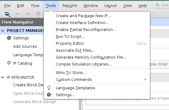
While using Vivado 2018.3, I went to the menu, and selected “Create and Package IP”.
 |
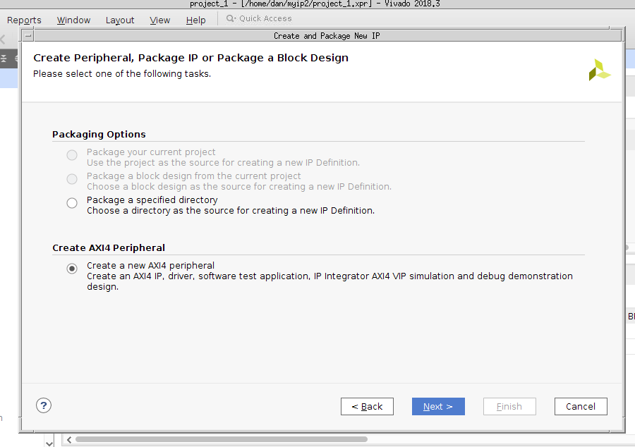
Vivado then brings up a dialog box, shown in Fig. 4, and I clicked through it.
 |
The second dialog box asks me what what type of IP I wish to create, shown in Fig. 5. I selected “Create a new AXI4 Peripheral.”
 |
The following dialog box asks me for a name and location for where this IP should be placed. If you do this, take careful note of the location–I’ve been surprised more than once that the location of the new IP isn’t within the current project and directory I’m working with. If you get stuck, just go back and re-create your IP, but noting the directory along the way. You can stop mid-way through this second time if you need to–once you know where the last IP got stored.
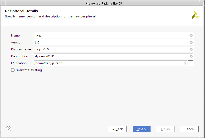 |
After this, you’ll finally come to an interesting dialog box, the one where you actually set up the parameters for and configure your core.
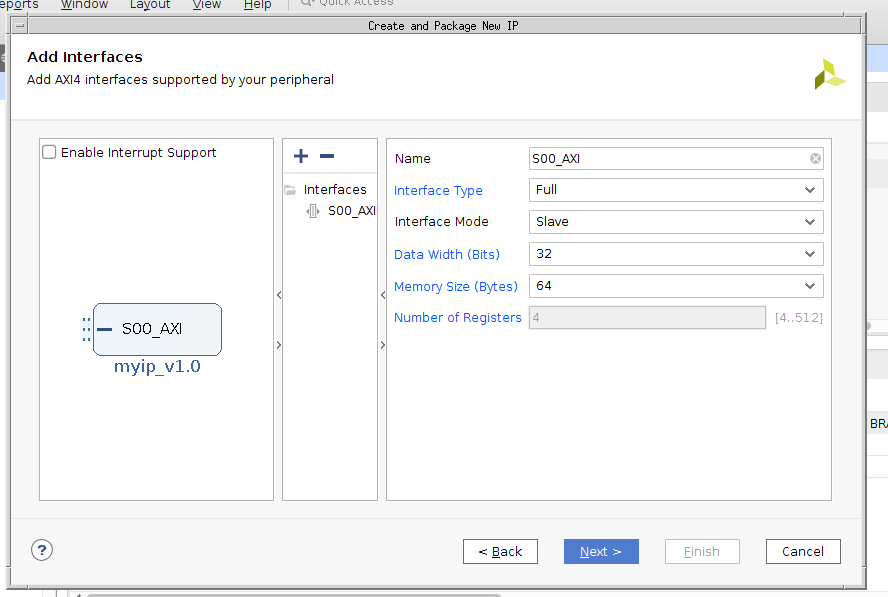 |
For the code we’ll be discussing today, I created a full AXI Slave peripheral with a 32-bit data bus and a memory size of 64-bytes (i.e. 6 address bits).
There’s then another dialog or two with information in them, and then
Vivado
actually generates the core we’ve requested. In my case, it generated a
directory of information, having subdirectories for bd, drivers,
example_designs, hdl, and xgui. There’s even a component.xml
file with a bunch of properties in it that look GUI related.
Looking around the rest of the directories, I found a lot of TCL files, some verification scripts, and even a C program which I assume would be used for verifying that this peripheral works.
Not finding any formal property files, I took these with a grain of salt.
I then discarded everything but the hdl directory. Within the hdl
directory, I found two files, of which only one has any significant logic
within it. I renamed this file, and then placed it within a github
repository where I could both work with
it and share my results with all of you.
This was then the
core
that I started working with, and that will form the basis for our discussion
below. With the exception of the ifdef FORMAL section and the
initial statements
just preceding it, I’ve kept it identical to what
Vivado
first created.
Verification IP Status
My current AXI4 verification IP (not posted) looks nothing like my previous attempt, or even those before it.
The list below is a sampling of some of the checks found within it. In
this list, I’m going to use * as a wildcard, so *VALID might refer to any
of the AWVALID, WVALID, BVALID, ARVALID, or RVALID signals.
I will also use the convention, found within the AXI
specification, of using x, as in
AxLEN, to refer to either write or read channel. Hence AxLEN could be
either AWLEN or the ARLEN signals. That said, here’s a sampling of
some of the checks within this new formal property core:
-
All
*VALIDsignals must be low initiallyXilinx’s slave core didn’t meet this property, since it didn’t initialize any of the registers within the core. I quietly added initial statements and moved on.
-
All
*VALIDsignals must be low following a reset -
Any time
*VALIDand!*READY, all associated properties must remain stable into the next clock cycle -
Read and write bursts must each be
AxLEN+1beats long, and end with anxLASTsignal -
BVALIDshall not go high unless first preceded by anAWVALID & AWREADYand then by aWVALID & WREADY & WLASTSimilarly,
BVALIDmay not go high with a givenBIDunless preceded by anAWVALID & AWREADYand anAWIDmatching thatBID, as well as all of the data associated with that burst.Put simply for every
AWVALID & AWREADYwith IDAWID, there should be one and only oneBVALID & BREADYresponse withBIDequal to thatAWID. -
RVALIDmay not go high unless first preceded by anARVALID & ARREADYSimilarly,
RVALIDmay not go high with a givenRIDunless, much like theBVALIDandBIDcriteria above, there has also been anARVALID & ARREADYwith that sameARIDon the clock prior.This is one of the more difficult specifications to meet, particularly when using induction. The particularly challenging piece is that a good interconnect or other master should be able to have multiple bursts outstanding at any given time. Worse, without induction, there’s no way to prove that a core won’t break between receiving its second
AxLEN=255transaction request. Induction is therefore practically required in order to prove that something works. -
Bursts may not cross 4kB boundaries
Passing induction with this criteria, but also without being able to use any multipliers (formal tools struggle with multiplies) can also be a challenge.
-
WSTRBcannot be high for all of the bits of an unaligned access. Depending upon the unaligned portion of the address, some of the bottomWSTRBmust be zero. -
No more than
1<<AWSIZEbits ofWSTRBare ever allowed to be highWhile this property will not impact today’s verification requirements, it has caught a variety of bugs in some of the interconnects I’ve verified. In particular, I’ve caught mis-routed write packets with this property.
-
AxBURSTvalues may only be FIXED (2’b00), INCREMENT (2’b01) or WRAP (2’b10). The reserved mapping of 2’b11 is disallowed -
WRAP transactions:
-
WRAP transactions must begin with an aligned address
-
Bursts of type WRAP must have lengths of 2,4,8, or 16
-
-
The
AxSIZEdescription of a transfer may not exceed the width of the interface. Since this design is for a 32-bit interface,AxSIZEmay never be more than3'b010.In today’s example, Xilinx’s demonstration AXI slave core can’t handle an
AxSIZEthat doesn’t match the bus size,(1<<(AxSIZE+3)) == C_S_AXI_DATA_WIDTH, even though the AXI protocol specifically supports it.If you want to support
AxSIZEs other then the one matchingC_S_AXI_DATA_WIDTH, you’ll need a core that has what’s known as “narrow burst” support, such as this one.You might find you require this support if you ever find yourself needing to support buses from multiple native sizes, with bridges between them. As an example, the DDR3 SDRAM implementations I’ve worked with have been natively either 64 or 128 bits wide, even though the ZipCPU is natively 32 bits wide.
-
The slave shall not respond with a value of
BID(orRID) that doesn’t correspond to a value previously given to it.This is the second very challenging specification to meet when using induction.
-
The formal verification properties also support a configurable number of maximum stall cycles. If set, the slave may not leave it’s associated
*READYline low for more than this many cycles if the respective*VALIDline is high. There are similar stall counters for both address channels as well as the write channel.These counters need to be tempered by back pressure. Hence, if
BVALID && !BREADYfor example, then the stall count onAWREADYis paused.These counters are all from the slave’s perspective, insisting that the slave stall the bus no more than the given number of cycles.
-
The core also supports two other types of counters. One set determines the maximum number of clock cycles the slave can take from request to response, while the second set constrains the amount of time the master can stall the return channel.
In each case, the limit can be set to zero to disable this logic.
These counters are important, since they can catch things like dropped packets–which we’ll see in a moment. They can also be a challenge, since they often force the number of steps in the proof to be at least as many steps as are in the counter.
As an example of when you might wish to disable the timers, consider my own AXI interconnect. In that case, if two masters each tried to request a maximum length burst from the same slave, one of them would’ve needed to wait more than 256 cycles. Keeping the proof within 5 clock cycles meant that I needed to disable this check.
-
The verification IP also offers address outputs, which can be used with either write or read data channels to verify that the responses are associated with the given address.
To support
Xilinx’s
demonstration core,
I also needed to create an OPT_NARROW_BURST option to my formal VIP. If
this parameter is set, the VIP will insist that AxSIZE corresponds to
C_S_AXI_DATA_WIDTH, no more and no less. While this isn’t part of the
AXI specification per se, Xilinx’s
demonstration
core
doesn’t have the logic within it to process bursts of any other AxSIZE.
Given that the difference between narrow burst support and no narrow burst
support is only about 36
LUTs, though, were this
my own core I would’ve probably sided with providing full bus support.
OPT_NARROW_BURST: Narrow burst support (C_S_AXI_DATA_WIDTH == (1<<(AxSIZE+3)))
The VIP core also has an option that can be set to indicate that the core
supports exclusive mode, OPT_EXCLUSIVE. This mode is associated with
the various AxLOCK flags. The idea, from an
AXI point of view, is that a read
transaction might set ARLOCK. The peripheral core may then return EXOKAY
indicating that it supports exclusive access. Some time later, the bus
master may issue a write transaction to the same address. At that time, the
core is to respond with EXOKAY if no one else has written to that address
between the read and write requests, or OKAY if the address has been written
to between the read lock and the write lock. In the case of an OKAY
response, the slave is required not to write to the value, but rather to leave
it alone.
I haven’t yet fully implemented the properties to check these exclusive access transactions. On the other hand, I don’t yet have a core that uses them, so this isn’t much of a problem yet, although the exclusive access features don’t appear to be all that hard to build. Certainly this demonstration core doesn’t support exclusive access, so it’s a moot point for this discussion.
Instead, I’ve implemented the following properties for cores that don’t support exclusive access:
-
Unless
OPT_EXCLUSIVEmode is set-
Slaves may not return a response of
EXOKAY -
Masters may not raise
AxVALID & AxLOCK
-
Moving on, I made one rather controversial choice having to do with WVALID.
I chose to set up the core so that WVALID may not be asserted before
AWVALID. The AXI4 protocol doesn’t
require this, although Xilinx’s
peripheral
enforces this internally. This rule just made the VIP easier to write: it
kept me from needing to verifying skid buffers for write address and write
data channels.
-
WVALID may not be asserted before AWVALID
- If writes are pending, to include when
WVALID & WLAST, AWREADY must be low - If
AWVALIDandWVALIDare asserted on the same clock cycle, thenWREADYmay not go high beforeAWREADY
- If writes are pending, to include when
Since this requirement goes beyond what AXI requires, and (worse) risks false positives, I will likely need to go back and revisit this requirement in the future.
Now, using all these properties, shall we spend a moment to take a look at Vivado’s demonstration core?
Read and Write Traces
Let me start out presenting their core by presenting read and write traces generated using the properties above. My purpose is to show an example of how the core is supposed to work. Be aware, however, that this is backwards of how I actually examined the core, but it makes for a good overview. I personally started examining this core by examining whether my assertions and assumptions held, but we’ll get to those in a moment.
I often think of an AXI read transaction as the simpler of the two, so let’s start with a read transaction and consider the AXI transaction in Fig. 8 below.
 |
Notice in this trace that ARREADY waits until after ARVALID goes high
to go high. Then, once the address has been accepted, the core returns one
value every other clock. As a result, any burst of N items will take a
minimum of 2+2N clocks to complete.
I was actually expecting much better performance than this from a [Full AXI slave core](his core](https://github.com/ZipCPU/wb2axip/blob/master/bench/formal/xlnxfull_2018_3.v). Isn’t the whole point of using burst transactions the ability to perform transactions at high speed without the connection overhead? Indeed, the AXI-lite slave core I built could perform better than this full AXI slave core, and for much less logic as well! Of course, this doesn’t mean that Xilinx’s interconnect could’ve driven my AXI-lite slave core any faster, it just means that the peripheral could’ve operated much faster. For all I know at this time, Xilinx’s core might have the same 2-clocks per beat requirement, or it might actually operate at one beat per clock. I haven’t gotten that far in my investigations. I do know that my own AXI interconnect can handle one beat per clock, although it does pay for this capability in logic usage.
 |
Fig. 9 on the right shows a burst write transaction.
Here, you’ll notice that, as before, AWREADY idles low and doesn’t go
high until after AWVALID is raised. While this is valid according to the
AXI specification, the
specification also recommends idling
with AxREADY high rather than low. However, once AWVALID & AWREADY
are both true, WREADY will go high on the next cycle. From that time forward,
the core
is able to handle one write beat per clock. Once the last write data value
has been received, the
core
raises BVALID. In total, this requires 3+N clocks per burst of N
beats. This is actually somewhat decent performance, primarily driven by
AXI requirement that all signals must be
registered.
At issue in our next section is the simple question of whether or not this core will reliably follow the AXI protocol. As we shall see, there are some serious flaws in its performance.
Bugs in Vivado’s AXI demonstration core
By my count, this core has three significant bugs within it, and one ridiculous eye-brow raising example of a plain old stupid piece of unnecessary and crippling logic.
1. The core might return the wrong ID
The first bug is associated with the ID logic.
In an effort to make packet routing simpler when using
AXI, each request
and response can be given an identifier, AxID. Then later, when the
slave responds, it is required to respond with the identifier found within
the request. Further, the slave is required to preserve packet ordering within
a given ID.
-
As an example of how this might be used, consider the DDR3 SDRAM protocol. It costs several clocks to switch from accessing one row of memory to another. Similarly, it takes several clocks to switch from reads to writes. On the other hand, if the DDR3 SDRAM controller could return responses out of order, it might be able to pack more accesses from a given row together before switching rows.
AXI IDs make it possible to return values out of order. The only rule is that, within a given ID, they must be returned in order.
At one time I used this property within my own WB to AXI bridge. I assigned each WB transaction to an address within a buffer, and then used this address as the transaction ID. This allowed me to interleave read and write transactions, to adjust transaction widths, and to receive transactions out of order on return. I’m now in the process of tearing this extra code back out, for the simple reason that it made the core way more complex than it needed to be.
-
The other example of where ID’s might be used is within the AXI interconnect. The AXI protocol is designed so that an interconnect might give all of the bursts from a given master a particular ID. Then, when the slave returns the response, the interconnect can then use the returned ID as part of a routing scheme so that the response from the slave is returned to the proper master.
That’s the theory at least.
I should note that when I built my own AXI crossbar interconnect, I was disappointed to learn that this feature wasn’t very useful. Allowing two separate masters to access the same slave already required a clock lost while arbitrating between the two of them. If I granted access to a particular master, and kept that grant active, I could optimize accesses from that master while all other masters would be forced to wait. Had I supported IDs, I’d need to suffer that clock lost to arbitration on every new request.
The problem is even worse than that. Not only would a clock be lost due to arbitration on every address channel request, there would be another clock lost due to arbitration on the return channel as well.
If that’s not enough, the necessary back pressure might have broken the core we are studying today–as I’ll explain shortly.
For all of these reasons, my own AXI interconnect supports IDs, but doesn’t use them during routing.
ID’s are also one of the special features present in AXI that are not present in AXI-lite. They’re one of the things that make the full AXI protocol special.
 |
In the case of Xilinx’s demonstration core, the formal tools returned a trace showing that transaction IDs were not properly preserved from request to response, as shown in Fig. 10 on the right.
With a little bit of digging, I found the bug. In this case,
the response ID wasn’t registered with AxVALID & AxREADY.
	assign S_AXI_BID = S_AXI_AWID;
	assign S_AXI_RID = S_AXI_ARID;
This is wrong on a couple of levels. First, once AxVALID & AxREADY are
true, the Ax* lines can be anything–such as a request for a second
transaction. Nothing requires the AxID values to remain constant. Indeed,
this bug might cause the response from the core to be misrouted to a master
that hadn’t requested it, while causing the rest of the design to hang waiting
for a request that would never come!
This is also one of those bugs that you wouldn’t likely find using the traditional test bench methodology, where you interact with a core as much as your imagination allows. For me, that was never more than one request at a time, or even one ID at a time. I know that I personally struggled to identify all of the possible failure modes in my own cores prior to using formal methods.
The fix, at least in this case, is really easy: register the return ID’s. Here’s the logic necessary for the write channel, the read logic would be similar.
	reg [C_S_AXI_ID_WIDTH-1:0]	s_axi_bid;
	always @(posedge S_AXI_ACLK)
	if (S_AXI_AWVALID && S_AXI_AWREADY)
		s_axi_bid <= S_AXI_AWID;

	assign	S_AXI_BID = s_axi_bid;
2. Logic depending on WLAST wasn’t guarded by WVALID
Consecutive AXI data bursts are
separated from one another by the xLAST
signal. Hence, as you saw in Figs. 8 and 9 above, the last data item was
marked by xLAST. Ideally, this would mean that the next burst might
start immediately on the next clock cycle, had the core been optimized
for throughput.
However, the xLAST signal is only relevant if the xVALID signal is also
true. If xVALID is false for a given channel, then all of the AXI
signals on that channel are don’t cares and irrelevant.
 |
While this may not be the most common AXI
mistake out there,
it certainly ranks up there: All AXI
signals are undefined unless the associated xVALID line is high.
Xilinx’s core didn’t follow this rule, as shown in Fig. 11 on the right.
In particular, several signals depended upon the presence of WLAST while
assuming that WVALID would also be true at the same time. In this case,
the core
went into an invalid state, dropping both WREADY and raising AWREADY for
the next burst, without ever returning a BVALID response. As a result,
the core
never finished reading the write data for this transaction.
If you look through the source code, you find some incomplete cascaded ifs. Here’s one example:
	always @( posedge S_AXI_ACLK )
	begin
	  if ( S_AXI_ARESETN == 1'b0 )
	    begin
	      axi_wready <= 1'b0;
	    end
	  else
	    begin
	      if (~axi_wready && S_AXI_WVALID && axi_awv_awr_flag)
	        begin
	          // slave can accept the write data
	          axi_wready <= 1'b1;
	        end
	      //else if (~axi_awv_awr_flag)
	      else if (S_AXI_WLAST && axi_wready)
	        begin
	          axi_wready <= 1'b0;
	        end
	    end
	end
(The comments above are not mine, but rather are provided with the generated code.)
Notice the first bug: the logic depends upon WVALID & WREADY and something
else! In a prior post, I declared this to be the most common AXI bug I’ve
come across.
The second bug is that
the core
checks for S_AXI_WLAST && axi_wready, rather than also checking for
S_AXI_WVALID as well. Had the logic block been written instead as,
	always @( posedge S_AXI_ACLK )
	if (!S_AXI_ARESETN)
		axi_wready <= 1'b0;
	else if (~axi_wready && S_AXI_WVALID && axi_awv_awr_flag)
		// slave can accept the write data
		axi_wready <= 1'b1;
	else if (S_AXI_WVALID && S_AXI_WLAST && axi_wready)
		axi_wready <= 1'b0;
it would’ve fixed the problem with this particular block. That would leave one remaining block still needing a similar fix.
As with the last error, the bus would come to a screeching halt if this ever happened in practice, with the bus master waiting forever for the response to its burst. Worse, if a second address request were made at this time, the original data would get written to the address associated with the second burst and … it just goes downhill from there.
I can only guess that Xilinx’s
interconnect,
the code of which I don’t have access to currently, doesn’t set WLAST
unless it also sets WVALID. I shudder to think of what might happen
if it didn’t guarantee this, or similarly if a “working” design were taken
from where it was working with one
interconnect
(Xilinx’s), and placed into another environment,
such as an ASIC
environment, which didn’t maintain this property.
3. Any backpressure on BREADY and the core will drop responses
The first rule of bus transactions is that every request gets a response. The second rule is that stalled requests are not allowed to change until they are accepted. In the case of AXI that applies to stalled responses as well–a condition referred to as back pressure.
What might cause back pressure? There might be back pressure if the interconnect ever needs to arbitrate between multiple competing return responses to a given master. Another possible cause of back pressure might be an interconnect that issued two transaction requests to different slaves, and is still waiting for the first slave to respond. A third reason might be a DMA controller that, having issued a read request of one peripheral, had also issued a write request to a second peripheral and is still waiting on second peripheral to accept the write data.
Back pressure, however, can be a challenge to deal with.
One of the difficult problems with back pressure is that with enough
back pressure, the AxREADY signals need to drop for the associated
address channels as well. Xilinx’s
core
in this case attempts to deal with back pressure by only raising the AxREADY
lines once the last transaction completes.
 |
Or rather, I think that was the designers intent. That’s not what the code
actually does. In the case of the write channel, Xilinx’s example
core
only waits until WLAST is high, then it will both set BVALID and
consider accepting a second burst. The problem is what happens if
BREADY isn’t also high at the same time, as shown in Fig. 12 on the right.
In this example, BREADY is low long enough that the second burst’s
write response to overwrite the response from the first burst. This could
easily halt a design depending upon this peripheral so hard it would take
a power cycle to fix.
Incidentally, Xilinx’s AXI-lite core had this same problem. While this core only suffers the problem on the write return channel, Xilinx’s AXI-lite core suffered from this same problem on both read and write return channels.
Their field engineer asked me about my AXI-lite conclusion. He pointed to an AXI-lite trace that was very similar to the one shown in Fig. 12 above, and then pointed out (correctly) that there was no protocol error shown in the figure. A slave might validly send write responses any time it wants, and so perhaps there’s a write response still waiting.
Here’s the critical piece of missing information: the final state shown in Fig. 12 is a STEADY STATE! The core never returns the second response.
What happened?
Let’s take a look at the logic block that sets AWREADY to see.
	always @( posedge S_AXI_ACLK )
	begin
	  if ( S_AXI_ARESETN == 1'b0 )
	    begin
	      axi_awready <= 1'b0;
	      axi_awv_awr_flag <= 1'b0;
	    end
	  else
	    begin
	      if (~axi_awready && S_AXI_AWVALID && ~axi_awv_awr_flag && ~axi_arv_arr_flag)
	        begin
	          // slave is ready to accept an address and
	          // associated control signals
	          axi_awready <= 1'b1;
	          axi_awv_awr_flag  <= 1'b1;
	          // used for generation of bresp() and bvalid
	        end
	      else if (S_AXI_WLAST && axi_wready)
	      // preparing to accept next address after current write burst tx completion
	        begin
	          axi_awv_awr_flag  <= 1'b0;
	        end
Did you see the bug? There’s actually a couple of bugs here. Let me give
the rest of the block here for reference, but the bug is in the if
statement(s) above.
	      else
	        begin
	          axi_awready <= 1'b0;
	        end
	    end
	end
The first bug is that this core checks for ~axi_awready && S_AXI_AWVALID
and something else. This is a common AXI
mistake,
probably created by the engineer wanting to make certain the other flags
are also true. The consequence of this bug, though, is that if the something
else wasn’t also true, then an address request just got dropped.
But that’s not the bug that caused the trace in Fig. 12 above.
The second bug is the check for S_AXI_WLAST && axi_wready. In this case,
we’ve already discussed the problem of referencing WLAST without also checking
WVALID.
That’s still not the bug that caused the trace in Fig. 12 above.
The bug in the trace above centers around the use of the axi_awv_awr_flag
to determine whether or not the core is currently processing a burst, or if
it can accept the next burst for processing. In this case, once
S_AXI_WLAST && wready were true the burst was marked complete and ready
for the next address. If the designer had instead checked for
BVALID && BREADY, it might have fixed this issue. However, in the designer’s
zeal to lower the latency of this core, they allowed axi_awv_awr_flag
(the write address valid flag) to drop one clock cycle too early.
The rest follows from Fig. 12 above: the having dropped the write address valid
flag, the core now accepts the next write request. It accepts and writes a
value to the core’s internal data structure, and then sets BVALID. Only …
BVALID is already set. Hence a return response is dropped.
Many pieces of hardware, ARM included, will wait for a missing burst return forever. As a result, this would mark the end of any fault-tolerant design–and the bug was in vendor code!
Lesson learned: never trust vendor code.
When I built my own AXI
core, I chose
instead to stall the WLAST cycle if BVALID && !BREADY were true. That
little bit of overlap also allowed my
design to fully
process an AXI write transaction at
one beat per clock across multiple bursts. That’s better performance than
this core
achieves, while also passing a formal verification check which
this core
doesn’t.
4. This core won’t handle concurrent reads and writes
Did you notice from the last piece of code that AWREADY depended upon not only
the axi_awv_awr_flag (the write address valid flag, indicating a write burst
is active), but also the axi_arv_arr_flag (the read address valid flag)?
if (~axi_awready && S_AXI_AWVALID && ~axi_awv_awr_flag && ~axi_arv_arr_flag)This means that the core will not accept any read transactions while a write transaction is ongoing.
 |
This one I don’t get. Indeed, this doesn’t make any sense to me. One of the key features of the AXI protocol, a key selling point if you will, is that it can handle both reads and writes at the same time.
Not this core.
When I tweeted about this bug, Piotr suggested the reason for this was that the core was implementing a single port RAM. Indeed, if your only information was the trace above that would make sense. However, if you look through the logic of this core you’ll discover a couple of things. First, the registers within the core are implemented with either block RAMs or flip-flops. Given the size of this core, at only 64-bytes, it would probably be implemented in flip-flops. Either way, both flip-flops and block RAMs can handle both reads and writes on the same clock in Xilinx devices. Then, just to make this more crazy, the core will allow both a read and write at the same time if the two requests show up at the same time. Similarly, if a read request shows up during a write request the core will process it.
The only justification I can possibly think of for this “feature” is that this was an unintentional oversight.
Removing the test for the axi_arv_arr_flag “fixes” this particular problem.
Conclusion
This is now the second of Xilinx’s demonstration designs that I’ve applied SymbiYosys to. Let’s just say that I’m not going to recommend either of these two Xilinx designs, and I’m certainly not going to recommend them to any beginners! I can’t really think of a worse nightmare, as a beginner, than to be struggling with non-functioning vendor code. I’d be looking every place other than the one with the bug! Worse, I wouldn’t know how to verify if any of my “fixes” worked–especially since Xilinx’s own verification procedures failed to find any of the bugs illustrated above.
If you would like a basic AXI4 design that you can start from and work with, you might wish to consider this design instead. Unlike my demonstration AXI-lite design, this AXI full core requires connectivity to a second (external) core with the actual read/write logic within. I chose this approach to make it easier to integrate this demonstration design into another of my designs that desperately needs the AXI performance.
If all goes well, this demonstration core may well be the next AXI core I blog about.
As for the formal properties that I used to find the bugs in this core, those are currently available for purchase as part of the SymbioticEDA Suite.
These bugs were reported to Xilinx on 16 May, 2019. As of Jan, 2020, they have not yet been fixed.
Now all these things happened unto them for ensamples: and they are written for our admonition, upon whom the ends of the world are come. (1 Cor 10:11)