
Adding an AXI-Lite interface to your Verilator test script
It should come as no surprise to anyone that I like working with
Verilator.
In sum: Verilator is faster than most if not all other Verilog simulators
out there. It achieves this
high speed in part by not supporting 1'bz or 1'bx, nor does it support
statements with delays in them like, “a <= #5 b;”. This doesn’t bother me
much, since delays and 1'bx values aren’t really synthesizable
anyway.
No, where Verilator really shines is in its software interface. With my own background in software, I feel at home working in software and so I feel at home working with Verilator. Using Verilator’s software interface, it’s been easy to integrate hardware emulation into my simulations. This is something we’ve covered before. Indeed, I’m not sure how I would have debugged a compressed video decoder without being able to visualize the resulting video to know if the core I was testing was working or not.
Verilator also shines when you are trying to simulate the interaction of a CPU with your design. No, it’s not quite everything I would want: what I really want for testing a CPU’s interface to my design is something where I can issue memory reads and writes to my design-implemented registers as though those registers were part of my own memory space. While we won’t quite get there with today’s example, we’ll get pretty close. We might even get close enough that with a little work you could directly port your C++ test program to your ZipCPU (or MicroBlaze/Nios/Zynq/SoC) and know that it’s going to work.
Today, I want to share with you how you might go about driving a Verilator simulation of your design from an AXI-Lite control port into the same design.
The Need
To understand why you might want to drive a
simulation
using an
AXI-Lite
control port, consider the task I was struggling with last month: I’d built an
AXI DMA
controller,
and it wasn’t passing all of my cover() checks.
That’s not good.
To make matters worse, it’s not often clear what causes a cover() statement to
fail. Unlike assertion failures, cover() failures don’t normally produce a
trace
identifying the line of code and the step in your
trace where your design first
failed. No, when a cover() statement fails it just fails.
You as the designer get to know which cover() statement failed, but not why.
Worse, cover() statements don’t fail until the formal solver has exhaustively
checked every one of the number of steps you’ve asked for to see if there’s
one, any one, possible way the cover() statement might be made true. Sorry,
there’s no early “I can’t get there” terminations.
Why might a cover() property fail? It might be that your logic is broken.
It might also be that your cover() property is broken, or that you aren’t
looking far enough into the future. (I suffered from both.) That said, after
six hours of running any tool, I’ve looked “far enough” into the future and
if the cover() property hasn’t passed, it’s time to figure out why not. Did
I say six hours? I’d prefer five minutes. Once things worked, 20 minutes
turned out to be sufficient–but that’s part of another story.
In my case, the cover() check was failing because
the DMA
was accomplishing most of the transfer and then hanging for certain
combinations of transfers needing realignment. Without a
trace
to see what was going on, I got lucky with a guess that figured out what
was happening. I don’t want to depend on getting lucky. I needed
another way of figuring out what was going on.
That’s just part of the story though.
The other part of the story is that I’ve recently finished building several DMA implementations, and I don’t really have a design that will showcase these components. These include new AXI S2MM, MM2S, and DMA (MM2MM) data movers.
But what kind of design would showcase multiple DMA components?
Obviously, we’d need some memory to transfer data to or from. Our AXI (full) demonstrator core should fit this role quite nicely.
The DMA cores also need a controller to tell them from where to make their copies, and how many bytes to copy. So we’ll need to add an AXI master test controller to this mix as well.
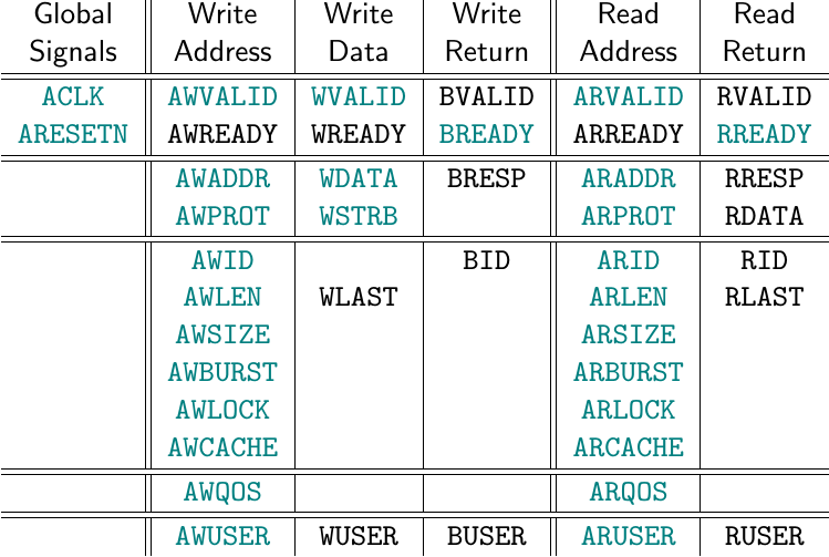
 |
Of course, random components don’t do anyone any good. Something needs to connect them together, and that’s the purpose of the AXI interconnect we’ll add into our test set as well. Such an interconnect can be used to arbitrate between which component had access to the bus at any given time. Normally, I’d say that’s too hard to do, but I’d recently built my own AXI interconnect, so let’s add trying that out to our to do list as well.
That gets us a touch farther along, but we’re not quite there yet.
 |
The problem is that each of my DMA cores has a control port to control the copy: where to to copy from, where to copy to, how much to copy, etc. This control port doesn’t support the full AXI protocol, but rather the AXI4-lite subset alone. My AXI interconnect doesn’t connect to AXI4-lite slaves. No, the AXI interconnect I’ve built will connect AXI4 masters to AXI4 slaves, not to a set of AXI4-lite control ports. If we want to interact with those various control ports, then we’ll need a bridge from AXI to AXI-Lite in order to drive these registers.
Ok, AXI to AXI-lite bridge, got that.
What else? How about an AXI-lite bus simplifier that can lump all of my AXI-lite peripherals together and act as a sort of AXI-lite crossbar?
 |
Ok, got that too.
What else?
 |
We’d also need a way of composing the entire design together. One of the sad realities of AXI is that with the number of wires that compose an AXI bus, just connecting two components together is a recipe for a lot of typing–not to mention a lot of errors should anything go wrong, and that’s only two components. To put something like this together, you’d need to connect at least eighteen AXI interfaces together and we’re not done yet.
This is the point where you can use Intel’s platform designer or Xilinx’s IP integrator. The problem is that, once you are done, you’ll have a design that can’t be used with Verilator, nor can it be easily moved from one FPGA (or ASIC) environment to another. No, a cross platform tool that allows us to keep our design in Verilog would be preferrable.
The good news here is that we can use AutoFPGA to connect AXI interfaces together. AXI support with AutoFPGA is still fairly new, but it would be worth checking out. (Hint: AXI support is currently only found in the dev branch.)
Those are the hard parts. The other details are easier.
The Stream Source
To test an AXI stream to memory
copy,
we’ll need a stream
source
in addition to our memory
component.
For this, a simple counter will work nicely. That will also allow us to measure
both how long the stream copy took, as well as whether or not any words were
lost along the way. The code for this is simple enough that we might just
want to copy it directly into our main design
file. We can
do that using the MAIN.INSERT tag in an
AutoFPGA
configuration file.
	always @(posedge i_clk)
	if (i_reset)
		@$(PREFIX)_tvalid <= 0;
	else
		@$(PREFIX)_tvalid <= 1;

	always @(*)
		@$(PREFIX)_tlast = 1;

	initial	@$(PREFIX)_counter = 0;
	always @(posedge i_clk)
	if (i_reset)
		@$(PREFIX)_counter <= 0;
	else
		@$(PREFIX)_counter <= @$(PREFIX)_counter + 1;

	always @(posedge i_clk)
	if (!@$(PREFIX)_tvalid || @$(PREFIX)_tready)
		@$(PREFIX)_tdata <= @$(PREFIX)_counter;
In this example,
AutoFPGA
will replace the @$(PREFIX) tags with the name of this
core.
Using name prefixes like this forms a sort of poor man’s variable scoping.
I say “poor man’s” since nothing really prevents another core from stomping
on these register names, since these lines will eventually all get pasted into
the same main.v
file as all of the other MAIN.INSERT blocks from all of the other components.
But what does this logic do? The most important parts are the counter and
the TDATA values. The counter always counts up on every clock tick,
eventually wrapping around at 2^32 clock ticks. The TDATA logic sets our
data to be equal to the counter any time the source isn’t stalled.
The result is that this stream source will gladly drop data values if the memory copy can’t keep up. Once the memory transfers start again, we’ll be able to tell from the counter how many clock ticks took place that did (or didn’t) transfer memory.
If you browse through the
configuration file,
you’ll notice only two other tags defined. Those are the PREFIX
tag,
giving a name to our element, and the
MAIN.DEFNS tag–allowing
us to copy
our register definitions to the top of our
main.v
logic file.
The Stream Sink
In a similar fashion, if we want to test a memory to stream copy, we’d need a stream sink. Perhaps we can build something that measures performance in this case, so that we can see how well and fast our copy works.
Remember, what’s the goal when working with FPGAs? Speed! That’s one of the reasons why you are using an FPGA in the first place, right? It’s also one of the greatest strengths of FPGAs. But what good is speed if you waste it on a poor bus implementation? For this reason, if none other, it would be worthwhile to check out via simulation just how fast the overall bus implementation is.
 |
What measures might we use? I picked three simple ones.
- The number of beats of information that have been transferred in total.
This would be a count of
TVALID && TREADYcycles. - The number of packets. This would be a count of
TVALID && TREADY && TLAST. - The number of clocks taken from the first beat to the last. This would be
a counter with a reset, that starts running upon the first beat of any
transfer, and whose value gets copied on any
TVALID && TREADYclock cycle.
For this, I’ll use a simple AXI-Lite slave, much like the Easy AXI-lite slave I posted a while back, but this time with our measures within it.
In this case, the
AutoFPGA
configuration file
also includes the information within it necessary to connect us to the
bus. First, we tell
AutoFPGA
that we want to be a slave of an AXI-Lite bus that I’ve named axil, and
that our design will have four addressable (word) registers within it.
@PREFIX=streamsink
@NADDR=4
@SLAVE.BUS=axil
@SLAVE.TYPE=DOUBLE
Moreover, the @SLAVE.TYPE=DOUBLE announces that this will be a simplified
AXI-lite slave that can share it’s bus logic with other AXI-lite
slaves.
Connecting this component to our design is as simple as instantiating the component within our design. It’s really just a matter of hooking wires up together. While this would normally be quite tedious, AutoFPGA attempts to simplify the task–as you’ll see in a moment.
We’ll first give our AXI stream
a name. The @$(PREFIX) of this component gives us a nice (hopefully) unique
name we can work with. (If it’s not unique, we can easily change it later.)
We can also define tags specific to this
configuration file,
sort of like local variables if you will. Here, we define the name of the
STREAM we are going to consume.
@STREAM=@$(PREFIX)Now when we reference @$(STREAM), it will get replaced with the name of this
component–currently set by the @PREFIX=streamsink statement
above.
The following MAIN.INSERT tag
then just copies logic into our
main.v
logic file, while substituting any @$(X) constructs with whatever the meaning
we’ve given to X is. That includes the clock associated with our bus, as
well as the reset signal for the bus.
	streamcounter #(
		.C_AXIS_DATA_WIDTH(32),
		.OPT_LOWPOWER(1'b1)
	) @$(PREFIX)i (
		.S_AXI_ACLK(@$(SLAVE.BUS.CLOCK.WIRE)),
		.S_AXI_ARESETN(@$(SLAVE.BUS.RESET)),
		//
		.S_AXIS_TVALID(@$(STREAM)_tvalid),
		.S_AXIS_TREADY(@$(STREAM)_tready),
		.S_AXIS_TDATA(@$(STREAM)_tdata),
		.S_AXIS_TLAST(@$(STREAM)_tlast),
		//
Now comes the hard part … enumerating all of those annoying AXI signals–most
of which we aren’t using anyway. To make this easier,
AutoFPGA
automatically defines a SLAVE.ANSIPORTLIST tag
for every bus slave. If we
just reference that,
AutoFPGA
will do the rest of the work for us.
		@$(SLAVE.ANSIPORTLIST)
	);
After variable expansion, these lines will get copied directly into our main.v file and we’ll be back to working in Verilog again.
We’ll need one more piece to this file before we are done with it, and that
is that we need to declare names for our three control words so that we can
reference their addresses by name
later. In this case, we have three control
words at offsets of 0, 4, and 8 bytes from the base address. We can
give these words names R_STREAMSINK_BEATS, R_STREAMSINK_PACKETS, and
R_STREAMSINK_CLOCKS.
@REGS.N=3
@REGS.0=0 R_STREAMSINK_BEATS   BEATS
@REGS.1=1 R_STREAMSINK_PACKETS PACKETS
@REGS.2=2 R_STREAMSINK_CLOCKS CLOCKS |
This stream sink component is now ready for assembly into the full DMA checking core.
Put together, though, we now have quite the shopping list of components to work with, as shown in Fig. 6. We’ve gone from needing to test just a simple set of DMA controllers, to a much larger, bigger, and more complex design. The DMA controllers needed memory, and then we needed a crossbar to tie all of our components together. Even that wasn’t enough, since we needed to control the AXI-lite control ports of the various DMA controllers, meaning that we also needed an AXI to AXI-lite bridge. We then added in our bus simplifier. What I haven’t mentioned is that, because I intend to drive this from an AXI-Lite script, I’m also going to need an AXI-lite to AXI bridge.
There’s only a little bit of requirements creep here, right? All that’s left now is the infamous “Some assembly required,” followed by giving it all a good shakedown to convince ourselves that everything really works like it’s supposed to.
Assembly
So, if we put everything together, here’s the system diagram I came up with.
 |
In this figure, I’ve tried to place the AXI masters above the crossbar and the slaves beneath it, but this approach falls apart somewhat for the simple reason that these DMA controllers are both masters and slaves. They have a full master interface for doing the memory copies, so I’d like to place them above the interconnect, yet they also have a control interface placing them as slaves below the interconnect.
Still, although it looks complex, it’s nothing more than what we discussed above. We’ve now got all of our parts and pieces in place. The project is a combination of cores from my WB2AXIP repository, together with a bit of simulation logic from a new repository to tie it all together. We’ve now used AutoFPGA to handle all of the bus compositing necessary to build a Verilog project. All that’s left is to drive the entire simulation from a C++ Verilator test script from the top.
What’s our purpose? Well, initially my purpose was to find out why the
cover() statements in my
AXI DMA
weren’t passing. Now that I’ve figured that out, though, I have some rather
grander visions. I’d like to see just how well memory copies like this can
perform. I’d also like a test bed where I can see how changes to one
part/piece/component affect other things.
 |
As an example of what I’d like to learn, one of the comments I see often on
Xilinx’s forums is, “Why doesn’t my [S/MM]2[MM/S]
memory core work?” Or even “Why won’t my (whatever core) copy multiple
packets?” My typical thought is, I’m not sure–what logic did Xilinx stuff into
their data movers
that would break them like that? I mean, my own packet logic is really simple:
for the most part it ignores any TLAST signals. Comments like this, though,
make me wonder if I shouldn’t be adding in something more for “better” TLAST
processing. I mean, if it works, it must not have enough features, right?
To make all of this work, we are going to need to be able to drive this entire design using an AXI interface into the Verilated design. Building this AXI interface to a Verilated design will be the subject of the rest of this article.
Building the AXI Interface
Some time ago, I presented my own vision for how an FPGA out to be controlled. This vision was presented in terms of a C++ interface that could then be used from test scripts or control programs to interact with the FPGA. Since that time, this vision has worked surprisingly well for me–so well in fact that I’ve hardly changed the interface since then. Indeed, the biggest changes have been adding more documentation to it–nothing more.
The basic control
vision
involves a C++ class
implementing an
interface to the
design. This
interface
has six primary functions. The simplest two are the
readio() function to read from a single memory address and the writeio()
function to write to a single memory address. There’s also a readi()
function to read from multiple addresses in a row as part of a burst,
and the similar writei() instruction. The last two functions, readz()
and writez() work the same as readi() and writei() save that they use
the same address for every read or write in the burst.
Under the hood, there are readv() and writev() functions that implement
the readi()/readz() and writei()/writez() pairs. This function either
increments the address between beats or … it doesn’t, depending upon a
argument given to it.
This is the
interface I
use when I want to interact with a design from an external serial port. I call
it the DEVBUS interface.
The steps to interacting with a design are then,
-
Some external program will call a class implementing these functions. Initially, this program is one I call wbregs that provides a command line based PEEK/POKE interface into the design. Eventually, though, as I work with the design, I’ll get tired of typing commands like this and make a shell script and then even replace that with a C++ program running coordinated testing.
We discussed how this testing progression typically went just recently, when I described how I go about bringing up a new hardware component. Ideally, you’d want to do it from simulation before hardware, and that’s what we’re discusing.
-
A library associated with a debugging bus converts these interface functions into a characters that can be sent over a serial port, and then sends them over a TCP/IP link. Ideally, this includes some type of compression and decompression as well.
-
A program then intercepts the other half of this TCP/IP link and either forwards the characters to the serial port of a device implementing my design, or (if it’s my simulation script) then to the emulated serial port in a simulated design.
-
Then, within the design, the byte stream is recomposed into transaction commands. If those commands were compressed, they are then decompressed. The result may then be sent into a FIFO, depending upon my implementation, and then into a bus interface.
-
Once the result comes back from the bus, it’s then (optionally) compressed and returned over the (possibly simulated) serial port, back over the TCP/IP link, and back to the software that sent the command.
This is how I normally do my debugging, and we’ve talked extensively about this interface on this blog. The good news is that, if you like this type of interface, I’ve recently written an AXI-lite master that can drive this “debugging bus”–instead of just the Wishbone interface I’ve traditionally used.
Today, though, that’s not what we’re going to build.
Instead, today I want to build a Verilator test script that will drive an AXI-lite interface but without the TCP/IP link in the middle. In many ways, this simplifies the process–we’ll no longer need the byte stream, the compression, the TCP/IP, etc. It’ll be easier to get us going that much faster.
However, there is one problem associated with doing things this way:
simulation
time. When using the
TCP/IP
interface,
simulation
time advances any time you aren’t transmitting anything. Today, though, we’ll
need to advance
simulation
time ourselves.
We’ll do that by calling our favorite tick()
function
to toggle the clock from within our simulation script. This works great
when your design only has one clock, but we’ll make a slight adjustment
to guarantee that we can support any
multiclock simulations
later on. This adjustment will guarantee that our
tick() method always toggles the
AXI
bus
clock.
To make certain that
simulation
time passes when we need it to, we’ll add an idle() function to
our interface
that just causes the design to move forward some predetermined number of
clock ticks.
The DEVBUS interface
also includes some number of
interrupt
processing functions as well:
-
There’s the
poll()function for determining if an interrupt has taken place. -
A similar
wait()function just sits in a loop waiting for an interrupt to take place. -
A third function,
usleep(), can also be used to wait on an interrupt.usleep()allows us to wait for an interrupt, while still timing out after some number of milliseconds in case the interrupt never shows up.
So here’s how this class structure will work:
 |
VMain
We’ll start off with the Vmain C++ class generated by
Verilator,
and any subclasses
Verilator
may choose to create. This class will faithfully implement our design logic
for us, from
main.v on down.
Our task will simply be to adjust the inputs and then call an
eval() function provided by the class to update any design outputs.
TESTB
We’ll then wrap that class with a TESTB
class providing
some helper functions, as shown in Fig. 9. This will give us access to a
tick() method that toggles our clock and advances simulation
time,
while also encapsulating any trace
file generation routines.
This class is automatically generated for us by
AutoFPGA,
to make sure that all clocks are properly
modeled for us.
MAIN_TB
This TESTB
class
will be wrapped by the MAINTB() class, also automatically
generated
by AutoFPGA.
This latter class will include any calls to emulator functions that you
tell AutoFPGA
to include. As you may recall,
AutoFPGA
is first a copy/paste
utility, and only then a bus compositor. Three particular
AutoFPGA
keys give you access to these functions. SIM.CLOCK
defines the clock your core needs
simulation
support at.
SIM.INIT
can be used to define any C++ variables
you need in
simulation,
can be used to initialize any of these variables, and
SIM.TICK
can be used to define any logic that might need to happen on a clock tick.
For example, I often like to define a serial port encapsulated by the class,
UARTSIM.
In the SIM.INCLUDE tag,
I’d reference the definition of my UARTSIM
class.
@SIM.INCLUDE=
#include "uartsim.h"
This would get placed at the top of the main_tb.cpp class file. A second
piece of logic,
SIM.DEFNS,
will be used to hold a pointer to an object of this serial port class.
@SIM.DEFNS=
	UARTSIM *m_@$(PREFIX);
Realistically, the name of the serial port could be anything–it doesn’t have
to include the PREFIX tag of this component at all. I could’ve just called
it UARTSIM *m_uart;. I just like to use the PREFIX tag here to help
provide some ability to separate device names. That way the same UART
configuration file can be used to define many UARTs, each with different
PREFIX tags.
Now that such a value is declared, the SIM.INIT
tag,
tells us how we need to initialize this value before any simulations start.
@SIM.INIT=
		m_@$(PREFIX) = new UARTSIM(FPGAPORT,UARTSETUP);
In this case, the FPGAPORT is a TCP port
number for this
serial port, and UARTSETUP captures the parameters of the UART–baud rate,
parity, stop bits, etc.
Finally, on every clock tick we’ll want to have our emulated serial port act on the data given to it.
@SIM.TICK=
		m_core->i_@$(PREFIX)_rx = (*m_@$(PREFIX))(m_core->o_@$(PREFIX)_tx);
Once variable expansion takes place, and assuming this components PREFIX
tag is given by uart, this will turn into the C++ statement,
m_core->i_uart_rx = (*m_uart)(m_core->o_uart_tx);The m_uart C++ object then emulates a serial port–given the output serial
port wire from the design, o_uart_tx, it produces the serial port input for
the next time step, i_uart_tx.
This is just an example of what you could do here. Other examples might include emulated video or audio inputs, outputs, and … well, the sky’s roughly the limit.
Supporting these emulation software calls is the purpose of the main_tb.cpp
wrapper. For today’s DMA testing design, though, we won’t be using any of
this emulation capability.
AXI_TB
We can now come to our AXI test bench
wrapper.
This is the part and piece of this design that I’d like to discuss in detail.
This C++ AXI\_TB class will need to wrap the main test
bench.
It will also provide us with simplified commands that we can use to access
the AXI bus within the design from the perspective of an
AXI master.
Let’s walk through this class definition in detail.
We’ll define this AXI\_TB class as a template class, defined using our test
bench software,
herein called TB. (This would be the software containing any emulation
layers that we just discussed before.) Based on our MAIN\_TB
test bench,
wrapping the TESTB helper
class,
we’ll make a copy of whatever it is into m_tb. If you’ve gotten lost in
this process, feel free to reference Fig. 9 above.
Here’s how this class definition starts out.
#include <stdio.h>
#include <stdlib.h>

#include <verilated.h>
#include <verilated_vcd_c.h>
#include "testb.h"

//
// devbus.h provides the definition of our common interface
#include "devbus.h"

//
// Number of clocks before deciding a peripheral is broken
const int	BOMBCOUNT = 32;

template <class TB>	class	AXI_TB : public DEVBUS {
	bool	m_buserr;
#ifdef	INTERRUPTWIRE
	bool	m_interrupt;
#endif
	VerilatedVcdC	*m_trace;
public:
	//
	// m_tb wraps the TESTB wrapper of the actual logic
	TB		*m_tb;

	//
	// A 32-bit unsigned integer is a bus word for our purposes today
	typedef	uint32_t	BUSW;

	bool	m_bomb;
Constructing one of these AXI test bench wrapper objects is straight forward. We primarily just create a simulation test bench wrapper within, and clear the (simulated) master’s AXI signals.
	AXI_TB(void) {
		//
		// Create a new test bench
		m_tb = new TB;

		//
		// Notify Verilator that we might turn tracing on later
		Verilated::traceEverOn(true);


		// On startup, nothing has timed out (yet)
		m_bomb = false;

		//
		// Before reset, all VALIDs must be zero.  We're also not
		// going to touch AxPROT again, so let's give it a useful
		// value going forward.  (Most of my designs have ignored
		// AxPROT so far.)
		//
		m_tb->m_core->S_AXI_AWVALID = 0;
		m_tb->m_core->S_AXI_AWPROT  = 0;
		m_tb->m_core->S_AXI_WVALID  = 0;
		m_tb->m_core->S_AXI_WSTRB   = 0x0f;
		//
		m_tb->m_core->S_AXI_ARVALID = 0;
		m_tb->m_core->S_AXI_ARPROT  = 0;
		//
		// Technically xREADY could be anything.  We'll set it to
		// zero as well.
		m_tb->m_core->S_AXI_BREADY  = 0;

		m_tb->m_core->S_AXI_RREADY  = 0;
		m_buserr = false;
#ifdef	INTERRUPTWIRE
		// If INTERRUPTWIRE is defined, it is defined to the
		// name of the interrupt output from the design.  If not,
		// we won't support interrupt logic.
		m_interrupt = false;
#endif
	}
Normally, the main_tb.cpp file offers us a function to open a VCD file for tracing the design. Since we’ve wrapped this interface, we’ll need to re-expose access to this function to the rest of the design.
	virtual	void	opentrace(const char *vcdname) {
		m_tb->opentrace(vcdname);
	}
More recently, I’ve allowed other traces to be generated other than VCD. At this point, the jury is still out whether or not the extra simulation time required to compress these other formats (primarily FST) is truly worth the wait.
The tick() method is fundamental. That said, it just calls an underlying
simulation tick method. The tick_clk() method
is similar. It keeps adjusting clocks and calling eval() on the underlying
model until the clock we are based upon, one called i_clk in this design,
actually toggles. Since we only have one clock in this design, tick_clk
is just a pass-through function
).
	void	tick(void) {
		m_tb->tick_clk();
#ifdef	INTERRUPTWIRE
		if (m_tb->m_core->INTERRUPTWIRE)
			m_interrupt = true;
#endif
	}
We’ll use a special reset() call to place the design into reset. This resets
all of the various *VALID signals and pulls ARESETN low.
	virtual	void	reset(void) {
		m_tb->m_core->S_AXI_ARESETN = 0;
		m_tb->m_core->S_AXI_AWVALID = 0;
		m_tb->m_core->S_AXI_WVALID  = 0;
		m_tb->m_core->S_AXI_ARVALID = 0;
One common user misunderstanding, when working with Xilinx cores, is that they don’t typically reset their entire designs within a single clock cycle. Indeed, Xilinx’s AXI implementations insist that the reset be held low for at least sixteen clock ticks.
		for(int k=0; k<16; k++)
			tick();
While my own designs rarely need these extra clock cycles, perhaps placing them here will make this AXI wrapper more versatile across designs.
There’s one other trick which isn’t obvious: once we clear the reset, we have to have a whole clock tick with the reset clear. (See Fig. A3-1.)
		m_tb->m_core->S_AXI_ARESETN = 1;
		tick();
	}
The next function, idle(cnt), is also a helper function. Because we are
running in a
simulated
environment, if you just call AXI read/write commands,
you might push the bus harder than you ever would in practice. For this
reason, idle() just holds the
entire design in an idle state for some number of counts.
	void	idle(const unsigned counts = 1) {
		m_tb->m_core->S_AXI_AWVALID = 0;
		m_tb->m_core->S_AXI_WVALID  = 0;
		m_tb->m_core->S_AXI_BREADY  = 0;
		m_tb->m_core->S_AXI_ARVALID = 0;
		m_tb->m_core->S_AXI_RREADY  = 0;
		for(unsigned k=0; k<counts; k++) {
			tick();
			assert(!m_tb->m_core->S_AXI_RVALID);
			assert(!m_tb->m_core->S_AXI_BVALID);
		}
	}
How many idle counts should you hold it for? One? Two? Twenty? That’s
between you and your design. Just remember, any call to idle(), or even
a failure to call idle() or to idle() for the right amount, might mask
an error within your core. For this reason–and many more which are common
to simulation in general–I wouldn’t trust this routine not to miss bugs
already existing within your
core.
For example, by just waiting for the bus protocol to complete any transaction, this simulation would miss the bug in Xilinx’s AXI Ethernet-lite core whereby writes to the core, if they showed up at the same time as a read request, would be applied to the read address. The moment you insist that your simulation only ever simulate reads or writes but never both, is the moment you abandon ever fully verifying your core in the first place.
Remember–use formal methods for verifying any bus based component.
But I digress. Today’s purpose is just to exercise a complex AXI-based design using simulation, and using a Verilator based simulation at that. It’s not to prove the design works, but rather just to demonstrate that we can interact with an AXI based design from a Verilator based simulation
The next thing we’re going to try is to read a value from memory.
When you consider the various classes of AXI masters I discussed earlier, this read method would fall in the class of a Single beat master. It issues a single beat request to your design, and then waits for the return.
Let’s see how we might do that. We’ll read one value from the AXI-lite bus
having
address a.
	BUSW readio(BUSW a) {
		BUSW		result;
		uint32_t	delay_count = 0;

		//
		// One of my first steps of debugging when a design doesn't
		// work, is to ask myself what AXI requests were taking place
		// or in progress.  This printf() gives me that kind of
		// context while the simulation is taking place.  In a longer
		// simulation, however, these printf's could get overwhelming,
		// so I just leave it commented here.
		//
		// printf("AXI-READM(%08x)\n", a);
The first step is to issue the request itself. This means setting ARVALID
and setting the requested
address
to the given one. We’ll clear the bottom two
address
bits
to make certain our
address
is aligned–it just makes things simpler.
(Remember, if you want to check for every condition, use formal methods
methods.)
		m_tb->m_core->S_AXI_ARVALID = 1;
		m_tb->m_core->S_AXI_ARADDR  = a & ~0x3;
		m_tb->m_core->S_AXI_RREADY  = 1;
Now we have to tick the clock and wait for S_AXI_ARREADY to go high.
Once it becomes set, we have to toggle one more time to make certain we’ve
completed the clock cycle with ARVALID && ARREADY.
		while(!m_tb->m_core->S_AXI_ARREADY) {
			tick();
			assert(delay_count++ < BOMBCOUNT);
		}

		tick();
When I first built this simulation wrapper, I didn’t include the delay_count
increment and assertion above. Then an mutant
core never raised ARREADY
and my
simulation
task just hung.
Wiser now, I’m using delay_count as a wrapper in every one of my loops
to make certain I never wait for any undetermined (infinite) delay. While
such an (infinite) delay might be legal under the
AXI protocol, it’s
certainly not what I would wish to allow.
Now that we’ve had one clock tick with ARVALID && ARREADY, we need to clear
ARVALID and our delay count. The next step is to wait for the RVALID
response. Again, we’ll count how long the peripheral takes to reply, and
make sure the peripheral replies within a reasonable number of clock ticks.
		m_tb->m_core->S_AXI_ARVALID = 0;
		delay_count = 0;

		while(!m_tb->m_core->S_AXI_RVALID) { // || !RVALID
			tick();
			assert(delay_count++ < BOMBCOUNT);
		}
Now that the slave has raised RVALID, we want to capture the the value to
return as our result. We’ll also check RRESP to see if a
bus
error
has taken place, whether a slave error or an interconnect error.
		result = m_tb->m_core->S_AXI_RDATA;
		if (m_tb->m_core->S_AXI_RRESP & 2)
			m_buserr = true;
Finally, we’ll let one more clock tick pass–the clock tick where
RVALID && RREADY, before returning the value returned from our design.
		tick();

		return result;
	}
Always be aware when you do this what state you are leaving the design in.
In this case, we left RREADY high. It’s not really a problem. RREADY is
a don’t care when nothing’s pending. It’s just something you want to be
aware of.
That function will read a single 32-bit value from the bus.
What if you want to read a 64-bit value from the bus? In this case, our bus is only 32-bits wide. We’d need to read two words in an incrementing fashion, and then merge the two into a single result.
	uint64_t read64(BUSW a) {
		uint64_t	result;
		int32_t		buf[2];

		readv(a, 2, buf);
		result = buf[1];
		result = (result << 32) | (uint64_t)buf[0];
		return result;
	}
Reading more than one value at a time is really the purpose of readv().
If you remember, we support three read calls internally: readio() reads a
single word, readi() reads some number of words while incrementing the
address, and readz() reads some number of words from a constant address–such
as a
UART or
my scope
might use. (I was once stingier with my address space
assignments.)
As I mentioned above, both readi() and readz() call a third function,
readv() to do the heavy lifting. That’ll be our next function to examine.
To use readv(), we’ll need
an address,
a number of words to read from, and a length. A fourth parameter, inc,
will tell us whether or not we want to increment
the address
or not.
	void	readv(const BUSW a, int len, BUSW *buf, const int inc=1) {
		int		cnt, rdidx, delay_count = 0;
As you might expect, the first step in a bulk read is to set ARVALID,
ARADDR, and RREADY. As before, we’ll trim off the lower address bits from
ARADDR, to force the read to be word aligned even though
AXI doesn’t necessarily require the
first word in any burst to be aligned.
		printf("AXI-READM(%08x, %d)\n", a, len);
		m_tb->m_core->S_AXI_ARVALID = 1;
		m_tb->m_core->S_AXI_ARADDR  = a & ~3;
		//
		m_tb->m_core->S_AXI_RREADY = 1;
At this point, we could probably do a burst read if this were an full AXI4
test bench interface, instead of just an AXI4-lite script. Were we to do
that, we’d also want to set ARBURST to either FIXED (if inc==0) or INCR
(if inc==1). ARSIZE would be set to the log (based two) of the
bus
width minus three (ARSIZE==0 for byte-width transactions, 1 for 16-bit
words, 2 for 32-bit words, etc.), so we would set that to 2. ARID could
be set to any integer with the right number of bits and just held constant. The
tricky one would be ARLEN. Nominally, we might set ARLEN to be len-1.
However, we’d have to adjust that since ARLEN can only go up to 255, and
that only if ARBURST == INCR. For a FIXED burst, ARLEN can only go up
to 15. That’s only the first constraint on ARLEN. The second constraint
on ARLEN would be that we can’t cross 4kB boundaries. In other words,
building a proper AXI4 burst would take some more work, but it is quite doable.
With a basic AXI-lite read request generator, things can be kept simple.
Let’s now keep track of how many reads we’ve requested in cnt, and the
index into our return arrow, kept in rdidx. Now we can start making
requests, until cnt==len and all requests have been made.
		rdidx =0; cnt = 0;

		do {
			int	s;

			m_tb->m_core->S_AXI_ARVALID = 1;
If ever, during this process, ARVALID && ARREADY, then a request has been
accepted by the
slave we are talking to–or,
rather, it will be accepted once the clock with ARVALID && ARREADY clock
tick completes. (Remember, we are peeking here at what happens just before
the clock tick.) Therefore, if ARVALID && ARREADY, we need to tick the
clock
once to make the request happen.
			s = ((m_tb->m_core->S_AXI_ARVALID)
				&&(m_tb->m_core->S_AXI_ARREADY)) ? 1:0;
			tick();
If a request was just accepted, then we’ll want to increment our address, and also increment the count of requests that have been accepted.
			m_tb->m_core->S_AXI_ARADDR += (inc & s)?4:0;
			cnt += s;
During this time, the slave
might also return values our way. If ever
S_AXI_RVALID && S_AXI_RREADY, then we’ll need to place a value into our
buffer. Remember, we’re holding RREADY high. Therefore, this means
copying data and increasing our buffer index, rdidx.
			if (m_tb->m_core->S_AXI_RVALID) {
				buf[rdidx++] = m_tb->m_core->S_AXI_RDATA;
				delay_count = 0;
			}
We’ll also reset our delay counter. This is the counter we’re going to use to determine if the slave is alive or dead–so that our simulation never hangs. If the slave responds at all, then the simulation isn’t dead. We’ll increment this counter in a moment–we just haven’t gotten that far yet.
We also need to check for any bus errors on return. For now, we’ll just record whether or not a bus error has taken place or not.
			if (m_tb->m_core->S_AXI_RVALID
					&& m_tb->m_core->S_AXI_RRESP != 0)
				m_buserr = true;
As the last step in our loop, we’ll increment delay_count and double check
that the slave
isn’t taking forever. (Remember, you can define BOMBCOUNT to
whatever is appropriate for your project at the top of this
file).
			assert(delay_count++ < BOMBCOUNT);
		} while(cnt < len);
The only unfortunate part about using an assertion like this is that the assertion will often fail before writing to any VCD file. Therefore, there’s a risk that the vital information you need in your VCD file about why things are failing might not make it in there.
This is why I routinely
flush any
VCD file
output routines during every call to move the clock forward, tick(). Perhaps
it slows down performance, but then again–the whole reason why I’m generating a
VCD file
in the first place is because I want to find problems like this, so
having the last little bit in them is important.
At this point in our processing, we’ve now requested all of the values we want
to read. The last step is to wait until the values we’ve requested come back.
Since this is
AXI-Lite,
they will come back in order. Similarly, if we’d held ARID constant, they’d
also come back in order–even if we were using the full AXI
protocol.
		m_tb->m_core->S_AXI_ARVALID = 0;
		delay_count = 0;

		while(rdidx < len) {
			tick();
When an item comes back, as marked by RVALID && RREADY, copy the value into
our buffer. We can also reset our delay counter here as well.
			if ((m_tb->m_core->S_AXI_RVALID)&&(m_tb->m_core->S_AXI_RREADY)) {
				buf[rdidx++] = m_tb->m_core->S_AXI_RDATA;
				delay_count = 0;
But if ever the response was not OKAY (zero), we then have a
bus
error.
				if (m_tb->m_core->S_AXI_RRESP != 0)
					m_buserr = true;
The last step is to double check that we aren’t stuck in an infinite loop waiting for a broken core to respond.
			assert(delay_count++ < BOMBCOUNT);
		}
We now have all of our values read, only the last RVALID && RREADY hasn’t
been clocked through the core (yet). That means we’re going to need one more
tick() of the clock before we shut RREADY down. Once that clock has
passed, our transaction should be complete. Therefore RVALID and BVALID
should both be clear–we’ll just double check that one more time to be certain.
		tick();
		m_tb->m_core->S_AXI_RREADY = 0;
		assert(!m_tb->m_core->S_AXI_BVALID);
		assert(!m_tb->m_core->S_AXI_RVALID);
	}
Remember, any bug you can find here is one less bug you need to find in hardware. That said, this core is not sufficient to prove that an AXI core is protocol compliant. In particular, we have done nothing here to double check that the core we are talking to can handle backpressure. Why not? First, because it’s not important to our simulation, and second because that’s much easier checked with formal methods.
Now that we know how to read a burst of items, we can define our two wrapper
functions: readi() which reads with an incrementing
address,
and readz() which reads multiple times from the same
address.
	void	readi(const BUSW a, const int len, BUSW *buf) {
		readv(a, len, buf, 1);
	}

	void	readz(const BUSW a, const int len, BUSW *buf) {
		readv(a, len, buf, 0);
	}
Unfortunately, AXI reads are much easier
than AXI writes. Handling write
transactions is going to be a touch harder, particularly because the master has
to allow the AW* and W* channels to get out of sync.
Let’s start with the single write transaction, writeio(), which requests
that a single word, v, be written to the
address,
a.
	void	writeio(const BUSW a, const BUSW v) {
		int	delay_count = 0;
Much as you might expect, we’ll start by setting AWVALID and WVALID
together. We’ll also force our
address
to be aligned, and set all of the
WSTRB values. (This routine only writes whole words–but it wouldn’t be
hard to adjust it to write half-words or bytes.) Finally, the all important
WDATA is set to the value we wish to write.
		// printf("AXI-WRITEM(%08x) <= %08x\n", a, v);
		m_tb->m_core->S_AXI_AWVALID = 1;
		m_tb->m_core->S_AXI_WVALID  = 1;
		m_tb->m_core->S_AXI_AWADDR  = a & ~3;
		m_tb->m_core->S_AXI_WDATA   = v;
		m_tb->m_core->S_AXI_WSTRB   = 0x0f;
Several individuals have recently posted to Xilinx’s forums wondering why
AWREADY never goes high for them. In their case, they were setting AWVALID
and waiting for AWREADY to go high before setting WVALID. Unfortunately,
many AXI slaves, like our own
even,
wait for AWVALID && WVALID before ever dropping AWREADY in the first place.
These cores might also hold AWREADY == WREADY, much as our
easy AXI-lite slave
did. You can avoid this problem by always setting
AWVALID and WVALID together. Indeed, the one core where I set WREADY
one clock after AWVALID && AWREADY slows my DMA checking design down.
Balancing the two channels with a
skid buffer (or two)
would probably fix this.
We now want to loop until both AWVALID and WVALID have been accepted, being
aware that the slave might accept them both together or individually and in
any order. Hence, we can’t wait for one and then the other–this wait needs
to be done in parallel.
		while((m_tb->m_core->S_AXI_AWVALID)
			&&(m_tb->m_core->S_AXI_WVALID)) {
			int	awready = m_tb->m_core->S_AXI_AWREADY;
			int	wready = m_tb->m_core->S_AXI_WREADY;

			tick();
If AWVALID && AWREADY, we’ll drop AWVALID: we’ve now made our write address
request. The same is true of WVALID && WREADY.
			if (awready)
				m_tb->m_core->S_AXI_AWVALID = 0;
			if (wready)
				m_tb->m_core->S_AXI_WVALID = 0;
A delay check at this point will also keep us from running into an infinite loop here in the case of a broken slave, so it’s a good thing to do.
			assert(delay_count++ < BOMBCOUNT);
		}
After making any write request it’s important to make certain that BREADY
is high, so that we might capture the write acknowledgment. Although we
didn’t set it initially, that’s not a problem. The write acknowledgment
isn’t allowed to come back before the slave has accepted both write address
and write data, so before this point BREADY is really a don’t care.
We’ll also clear our delay count–since the slave has fully replied to us.
		m_tb->m_core->S_AXI_BREADY = 1;
		delay_count = 0;
The last step is to wait for BVALID, the acknowledgment from the slave.
		while(!m_tb->m_core->S_AXI_BVALID) {
			tick();
			assert(delay_count++ < BOMBCOUNT);
		}
Once the slave acknowledges the write, we’ll check for any
bus
errors,
but
otherwise push the BVALID && BREADY cycle through with one more clock tick.
		if (m_tb->m_core->S_AXI_BRESP & 2)
			m_buserr = true;
		tick();
	}
While we could drop BREADY here, it’s not necessary. As I mentioned above,
if nothing is pending then BREADY is really a don’t care.
That’s what it takes to write one value and wait for a response. It was a little more complicated than reading, simply because the write address and write data channels could be out of sync.
What if we wanted to write a 64-bit value? That’s the purpose of writei()
(write with incrementing
address).
There’s also writez(), just as with readi() and readz().
	void	write64(const BUSW a, const uint64_t v) {
		uint32_t	buf[2];
		// printf("AXI-WRITE64(%08x) <= %016lx\n", a, v);
		buf[0] = (uint32_t)v;
		buf[1] = (uint32_t)(v >> 32);
		writei(a, 2, buf);
	}
Both writei() and writez() are handled by a third function, writev(),
which writes a burst of data to an (optionally) incrementing
address.
	void	writev(const BUSW a, const int ln, const BUSW *buf, const int inc=1) {
		unsigned nacks = 0, awcnt = 0, wcnt = 0, delay_count = 0;
Personally, I think AXI became unnecessarily
complicated
when they 1) split the write address channel from the write data channel,
2) created the AxLEN burst field, and 3) the AxBURST address
algorithms.
Yes, I know, certain pieces of hardware can handle bursts better than they can handle singletons. Having written controllers for SDRAM’s and flash devices, I’ve been able to achieve 100% throughput using such a simplified bus structure, and even done so with much lower latency due to a simpler bus implementation.
Did I mention that the AXI5 specification is even more complex than the already overly complex AXI4 specification?
But, you know, who am I to complain?
On to burst writes. As with singleton writes, our first step is to set
AWVALID and WVALID at the same time. Everything else here at this point
is roughly the same as it was for writeio() above.
		// printf("AXI-WRITEM(%08x, %d, ...)\n", a, ln);
		m_tb->m_core->S_AXI_AWVALID = 1;
		m_tb->m_core->S_AXI_AWADDR  = a & ~3;
		m_tb->m_core->S_AXI_WVALID = 1;
		m_tb->m_core->S_AXI_WSTRB  = 0x0f;
		m_tb->m_core->S_AXI_WDATA  = buf[0];
		m_tb->m_core->S_AXI_BREADY = 1;
		m_tb->m_core->S_AXI_RREADY = 0;

		do {
			int	awready, wready;
Where things start to get different is within our loop. For example, we now
need to issue ln AWVALIDs and ln WVALIDs, and these won’t necessarily
be in sync with each other. We can use awcnt therefore to count
the number of AWVALIDs that have been accepted, and wcnt to do the same
but for writes. That allows us to set WDATA to the right location from
within our buffer, and AWVALID and WVALID based on whether or not the
full ln number of requests has been received on each channel.
			m_tb->m_core->S_AXI_WDATA   = buf[wcnt];

			m_tb->m_core->S_AXI_AWVALID = (awcnt < (unsigned)ln);
			m_tb->m_core->S_AXI_WVALID  = (wcnt < (unsigned)ln);
As before, we’ll take a peek at what awready and wready are before the
actual clock tick,
so we’ll know what’s going to happen on this clock
tick.
			awready = m_tb->m_core->S_AXI_AWREADY;
			wready  = m_tb->m_core->S_AXI_WREADY;

			tick();
Once the clock has
ticked,
we can adjust our counter for the AW* channel. If the channel is live, we’ll
clear our delay count. Finally, if we are incrementing an
address,
we’ll update AWADDR.
			if (m_tb->m_core->S_AXI_AWVALID && awready) {
				awcnt++;
				delay_count = 0;
				// Update the address
				m_tb->m_core->S_AXI_AWADDR += (inc)?4:0;
			}
Advancing the write data channel is almost identical to the write address
channel above. If a piece of write data was accepted,
we’ll update wcnt and clear the delay counter. Note that we don’t need to
adjust WDATA here. Although we might, we’ve already set WDATA earlier in
this loop, so doing so here as well would be redundant.
			if (m_tb->m_core->S_AXI_WVALID && wready) {
				wcnt++;
				delay_count = 0;
			}
Unlike the writeio() routine, we need to check whether or not we receive
any acknowledgments while issuing requests. On any acknowledgment, we’ll
update our acknowledgments counter. On any acknowledgment indicating a
bus
error,
we’ll also set our bus
error
flag.
			if (m_tb->m_core->S_AXI_BVALID) {
				nacks++;

				// Check for any bus errors
				if (m_tb->m_core->S_AXI_BRESP & 2)
					m_buserr = true;
			}
Two comments here about
bus
errors.
First, we checked for RRESP == 0 above,
and BRESP & 2 here. It is illegal for an AXI-lite slave to return an
xRESP value of 1 (EXOKAY), so the two are equivalent. Indeed, this latter
test might take up less hardware and so be cheaper–in hardware. Here in
software, it might actually be costlier. Second,
unlike Wishbone
where we could halt an operation on a
bus
error,
we’re not going to do that here. While we might clear WSTRB on a
bus
error,
we’ll just note it and go on. How we actually deal with
bus
errors
will depend upon if the calling C++ test
script
checks for m_buserr or not.
Finally, we’ll increase our loop counter to catch any design that might hang, and loop as long as either the number of write addresses or write data transactions are less than our desired length.
			assert(delay_count++ < BOMBCOUNT);
		} while((awcnt<(unsigned)ln)||(wcnt<(unsigned)ln));
Once all write address and write data transaction requests have been made,
all that remains is to wait for the last acknowledgments to come through.
We’ll drop AWVALID and WVALID, and then look for BVALID.
		m_tb->m_core->S_AXI_AWVALID = 0;
		m_tb->m_core->S_AXI_WVALID  = 0;
		while(nacks < (unsigned)ln) {
			tick();
If (when) our BVALID acknowledgments come back, we’ll process them as before.
			if (m_tb->m_core->S_AXI_BVALID) {
				nacks++;
				delay_count = 0;
				if (m_tb->m_core->S_AXI_BRESP & 2)
					m_buserr = true;
			}
Perhaps I should be checking for BVALID && BREADY here. The difference would
only be a pedantic one, though, since I’ve already guaranteed (above) that
BREADY will be high whenever we are waiting on a response from the core.
The last step is our loop counter, and the one last tick that would accept
the BVALID noted above.
			assert(delay_count++ < BOMBCOUNT);
		}

		tick();
We’ve now completed our burst. Let’s clear up the bus, and just double check that it’s clear like we are expecting it to be.
		// Release the bus
		m_tb->m_core->S_AXI_BREADY = 0;
		m_tb->m_core->S_AXI_RREADY = 0;

		assert(!m_tb->m_core->S_AXI_BVALID);
		assert(!m_tb->m_core->S_AXI_RVALID);
		assert(!m_tb->m_core->S_AXI_AWVALID);
		assert(!m_tb->m_core->S_AXI_WVALID);
	}
The next two routines, writei() and writez(), are simple references
to writev above–that makes them easy.
	void	writei(const BUSW a, const int ln, const BUSW *buf) {
		writev(a, ln, buf, 1);
	}

	void	writez(const BUSW a, const int ln, const BUSW *buf) {
		writev(a, ln, buf, 0);
	}
In the tick() method above, we checked whether an
interrupt
wire (if defined) were true, and set a flag m_interrupt if it were. We
can come back later and poll() this value to see if an
interrupt
has taken place.
	bool	poll(void) {
#ifdef	INTERRUPTWIRE
		return (m_interrupt)||(m_tb->m_core->INTERRUPTWIRE != 0);
#else
		return false;
#endif
	}
Alternatively, we might wait some number of clock cycles for an
interrupt.
That’s the purpose of this usleep() method. It runs our design for some
maximum number of clock cycles, until an
interrupt
has been received.
	void	usleep(unsigned msec) {
#ifdef	CLKRATEHZ
		unsigned count = CLKRATEHZ / 1000 * msec;
#else
		// Assume 100MHz if no clockrate is given
		unsigned count = 1000*100 * msec;
#endif
		while(count-- != 0)
#ifdef	INTERRUPTWIRE
			if (poll()) return; else
#endif
			tick();
	}
A riskier approach might be to wait without a limit. Since I’m usually sitting at a keyboard with a control-C key waiting me, this hasn’t been a problem (yet).
	void	wait(void) {
#ifdef	INTERRUPTWIRE
		while(!poll())
			tick();
#else
		assert(("No interrupt defined",0));
#endif
	}
};
If you use this routine, always keep an eye on the size of any VCD file you might be generating. They can grow many GB quickly.
While today’s DMA test script isn’t going to use these routines, it certainly could.
The Simulation Script
Now that we’ve seen how we might issue transactions to an AXI slave from a C++ Verilator script, let’s turn our attention to the Verilator script itself, and see how this all worked out.
We’ll use a couple of macros to help drive the script. One of them is this
test bench RAM macro, or TBRAM for short. With this macro, we can then
treat the RAM elements within the design as though they were actually
elements of our C++ project–which in effect they are.
To get to the TBRAM definition, we’ll first need to define an
AXIRAM
macro to get us from the
Verilator
design to the
AXI block RAM.
#define	VVAR(A)	main__DOT_ ## A
#define	AXIRAM	VVAR(_axiram_mem)
We can then define a second macro to reference this one at the top of our test script.
#define TBRAM m_tb->m_core->AXIRAMOur memory to
stream
test will transfer data coming from MM2S_START_ADDR, and it will transfer
MM2S_LENGTH bytes.
#define	MM2S_START_ADDR		0x24
#define	MM2S_LENGTH		32768 // 262144
We’ll keep track of the same values, but in word addressing and word lengths, just to simplify things later.
#define	MM2S_START_ADDRW	(MM2S_START_ADDR/4)
#define	MM2S_LENGTHW		(MM2S_LENGTH/4)
The commands to interact with the MM2S module are listed at the top of the module itself. From there, we can draw these commands from it that we might use.
#define	MM2S_START_CMD		0xc0000000
#define	MM2S_ABORT_CMD		0x6d000000
#define	MM2S_CONTINUOUS		0x10000000
We’ll then repeat this work for the stream to memory test description.
#define	S2MM_START_ADDR		0x30
#define	S2MM_LENGTH		32768 // 262144
#define	S2MM_START_ADDRW	(MM2S_START_ADDR/4)
#define	S2MM_LENGTHW		(MM2S_LENGTH/4)
#define	S2MM_START_CMD		0xc0000000
#define	S2MM_ABORT_CMD		0x26000000
We’ll repeat similar definitions for the regular memory to memory DMA as well.
#define	DMA_START_CMD		0x00000011
#define	DMA_BUSY_BIT		0x00000001
// Extra realignment read (only)
// #define	DMA_SRC_ADDR		0x00000203
// #define	DMA_DST_ADDR		0x00008201
// #define	DMA_LENGTH		0x00000401
//
// Extra realignment write
#define	DMA_SRC_ADDR		0x00000201
#define	DMA_DST_ADDR		0x00008202
#define	DMA_LENGTH		0x00000403
From here, we’ll skip some of the boiler plate necessary to getting Verilator up and running, and for optionally recording results to a VCD file.
Let’s jump instead to right after our reset.
tb->reset();We’ll then start a test of the MM2S module by setting the RAM to known values. (A basic increment.)
	//
	// Test the AXIMM2S
	//
	memset(tb->TBRAM, -1, RAMSIZE);
	for(int k=0; k<MM2S_LENGTHW; k++)
		tb->TBRAM[k+MM2S_START_ADDRW] = k;
We can then set the address to transfer from, and the length of the transfer.
	tb->write64(R_MM2SADDRLO, (uint64_t)MM2S_START_ADDR + R_AXIRAM);
	tb->write64(R_MM2SLENLO,  (uint64_t)MM2S_LENGTH);
Let’s take a peek at what that first write64() transaction looks like, shall
we?
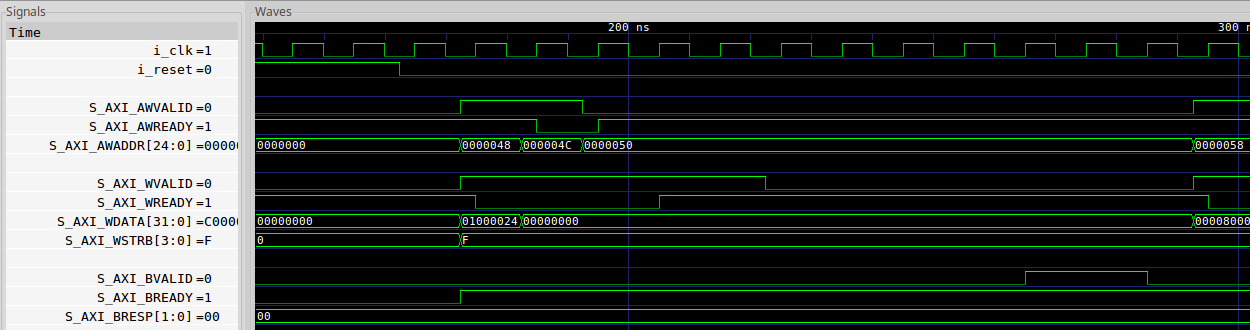 |
There’s a lot going on here, and it’s not all that apparent from this short trace. Let me walk you through it.
First, don’t get thrown off, but the changes we make from the test bench don’t happen on the clock. They happen just before. This puts them a little bit out of sync with the test bench itself, but if you look carefully you can see what’s going on in this trace.
What’s going on is that this request must first go through the
AXI crossbar. The
crossbar
needs to decode the address
request,
and then arbitrate among all of the possible masters to get access to the
bus. Hence it accepts the
AW* transaction immediately. The next AW* transaction, and even the first
W* transaction, both get stuck in the
skid buffers for several
clocks while arbitration takes place. Once the channel grant has been given,
the transactions can then come out of the
crossbar
and go into the AXI to AXI-lite
bridge.
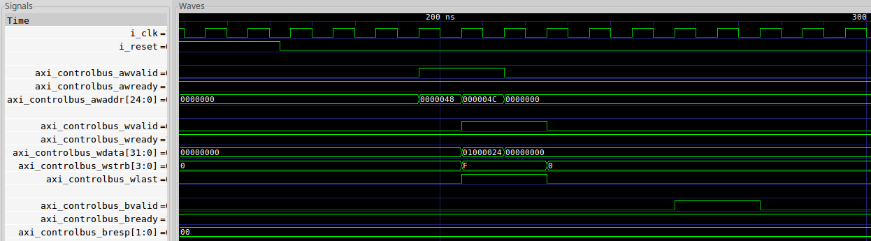 |
All parts of the transaction now appear to line up with the clock.
The AXI to AXI-lite bridge produces it’s output about a clock later, going into the AXI-lite simplifier. This bridge handles any and all AXI addressing, as well as reflecting any AXI ID values from request to response via a FIFO.
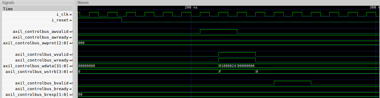 |
Once we come out of the simplifier, we now have an AXI-lite transaction going directly to our AXI MM2S control port.
 |
Did you notice through all these calls how the distance between AWVALID
and BVALID got successively shorter as we worked our way through these
traces? Remember, there are no
combinatorial paths allowed in AXI components between inputs and outputs.
That means that there must be at least one clock edge between any inputs and
their respective outputs. The result is that every AXI to AXI bridge costs at
least two clock cycles. In the end, writing just two values took 12 clock
cycles, or 120ns if we assume a 100MHz clock.
Ouch, but that’s what we’ll have to deal with if we want to play with AXI and go through bus bridges. There’s always a cost.
As a last step before kicking off our memory to stream copy test, we’ll reset the stream sink AXI-lite core that’s going to record how we’re doing and account for any missed values. We can also record the current clock.
	tb->writeio(R_STREAMSINK_BEATS, 0);
	start_counts = tb->tickcount();
The last step is to issue the start command and … they’re off!
tb->writeio(R_MM2SCTRL, MM2S_START_CMD);We’ll then sit back and wait for the copy to finish.
	while(tb->readio(R_MM2SCTRL) & 0x80000000)
		;
How’d we do? We can read the results right from the design using the readio()
method from above.
	printf("AXIMM2S Check:\n");
	printf("\tBEATS:  0x%08x\n", tb->readio(R_STREAMSINK_BEATS));
	printf("\tCLOCKS: 0x%08x\n", tb->readio(R_STREAMSINK_CLOCKS));
	printf("\tCOUNTS: 0x%08lx\n", tb->tickcount()-start_counts);
If you are interested in the timing of this readio() command, feel free to
try the test bench out and see for yourself.
I’m more interested in the report: 0x2000 or 32768 beats written in as
many clock cycles. We can also see that there were another 0x27, or
39 clocks, used between starting the core and the first beat that was
transferred.
AXIMM2S Check:
	BEATS:  0x00002000
	CLOCKS: 0x00002000
	COUNTS: 0x00002027
That’s a trace worth examining, so let’s take a peek at how this large transfer looked.
 |
Here you can see the whole purpose of this exercise, finding out how well the
AXI MM2S core
worked. The core
is designed so that it never issues more read
requests than what it has space in its FIFO, so you’ll see above as soon as
space opens up for the results from an AXI burst a new read request is issed.
You’ll also notice that these read requests are for ARLEN=8'hff or 256
beats at a time. That’s full speed.
Even better, did you notice that RVALID && RREADY hold constant? That’s
right! Once RVALID && RREADY go high, this
AXI MM2S core
is able to keep the
bus
busy at full speed transferring data. Our goal, 100% throughput, has been
achieved!
Well, it’s not that simple. Getting 100% throughput through the AXI MM2S core was only part of the battle. We also needed an AXI slave that could handle 100% throughput, as well as an AXI crossbar that could do it as well. This is indeed one of those cases where your performance will only ever be as fast as your weakest link.
There are a couple other tests of the MM2S core, but I’d like to move on to see how the S2MM core works.
In this case, the setup is nearly the same. We’ll write a starting address and a length to the S2MM core, and then tell it to go. We’ll then wait for it to complete.
	//
	// Test the AXIS2MM
	//
	memset(tb->TBRAM, -1, RAMSIZE);
	tb->write64(R_S2MMADDRLO, (uint64_t)S2MM_START_ADDR + R_AXIRAM);
	tb->write64(R_S2MMLENLO,  (uint64_t)S2MM_LENGTH);
	start_counts = tb->tickcount();
	tb->writeio(R_S2MMCTRL, S2MM_START_CMD);
	while((tb->readio(R_S2MMCTRL) & 0x80000000)==0)
		;
	while(tb->readio(R_S2MMCTRL) & 0x80000000)
		;
How many counts did it take us from start to finish? Let’s check our internal clock counter, and then check for any error codes that the core might report.
	printf("AXIS2MM Check:\n");
	printf("\tCOUNTS: 0x%08lx\n", tb->tickcount()-start_counts);
	printf("\tERR-CODE: %d\n", (tb->readio(R_S2MMCTRL)>>23)&0x07);
We can also check to see if any values were corrupted. For example, we can check that the values whose addresses occur before our memory write address remain at -1.
	for(unsigned k=0; k<0x30>>2; k++)
		if (tb->TBRAM[k] != (unsigned)(-1)) {
			printf("Pre-corruption: AXIRAM[%d] = 0x%08x\n", k, tb->TBRAM[k]);
			fail = true;
		}
Remember how our stream source was a counter? That means that we can walk through the values that were transferred looking for any dropped data. Indeed, any deviation from being a one-up counter will let us know of a dropped value or, if not, whether we truly did manage to send continuous values from start to finish.
	for(unsigned k=1 +(0x30>>2); k<(0x30>>2)+(16384>>2); k++)
		if (tb->TBRAM[k] != tb->TBRAM[k-1]+1) {
			printf("Result: AXIRAM[%d] = 0x%08x != 0x%08x + 1\n", k, tb->TBRAM[k], tb->TBRAM[k-1]);
			fail = true;
		}
Here’s where sending and receiving a counter helped–we had a known input, and we could verify a known output. The result?
No data lost! That’s a good sign.
But what I really want to know about is performance. How well did this design perform, with all of its parts and pieces?
AXIS2MM Check:
	COUNTS: 0x00002171
	ERR-CODE: 0
That’s not nearly the high speed performance that the memory to stream core achieved. What happened? Both were designed to be able to achieve 100% throughput.
To know that answer, we’ll need to take a peek at the trace recording this transfer.
 |
From this trace, you can see that
the S2MM core
is issuing maximum length
packets, over and over, much as we might expect. However, unlike before
where RVALID && RREADY stayed unbroken for the whole transfer, this data
transfer isn’t continuous. Sure, after the first burst, WVALID holds high
but WREADY doesn’t. Something is slowing us down. If we want to find out
what’s going on, then we’ll need to do a bit of digging.
Let’s zoom in on a new burst cycle once the design is fully loaded and take a peek at what’s going on there.
 |
Let’s start pulling this together from the end of the last burst. This end is
marked by the WLAST signal. Here you can see WLAST is true first coming
out of the
S2MM core,
and then on the next cycle it’s true coming out of the
crossbar.
A one cycle latency is as good as it gets.
The AXI S2MM
core
then sets AWVALID on the next cycle, right after WLAST was true. This is
good, and a nice sign of 100% throughput from the S2MM
core. This new
burst then starts with a new WVALID on the same cycle as well, also as coming
out of the S2MM
core,
so we’re still doing good here.
Until we aren’t.
The first problem is that the
crossbar has a two cycle
latency on the AWVALID, not just the one cycle on WVALID. The
crossbar
also holds onto the W*
channel until after AWVALID is sent–notice when axi_axiram_wvalid goes
high–it’s one clock cycle AFTER AWVALID gets received by the
block RAM slave.
Worse, the block RAM slave we
are using takes a second clock cycle after AWVALID before releasing WREADY.
That means we just lost three clock cycles on this single burst. These
clock cycles were do to the fact that each of these cores wanted a different
alignment of the W* channel.
2020-04-08 update: One clock was lost in this process due to the block RAM slave’s skid buffer being configured with
OPT_OUTREGenabled. DisablingOPT_OUTREGadvanced when the block RAM slave raised it’sWREADYsignal by one clock. This resulted in a 30 clock savings overall.
Here’s where an “AXI Slice” might come in handy. Had there been enough
slices to delay the W* channel so that it matched the delays in the AW*
channel, I might’ve been able to keep the W* channel fully loaded. No,
I don’t need any Xilinx AXI register slices to do this, the
skid buffer
with it’s registered output option should work quite well for this purpose.
Balancing those two channels will be one of my next tasks–or maybe placing this onto actual hardware. We’ll see. Since this work isn’t really funded, I might also end up sitting on it for a while too.
Conclusion
As you can see, it is quite possible to build and test an AXI design without needing a proprietary tool set. Even better, we were able to fully build and simulate such a design from a high level using Verilator. What we discovered, by drilling through and around the design, was that we could trace what happened to our AXI transaction(s) on every clock cycle.
Not bad.
My purpose today, though, was just to share the AXI test bench script that I used to gain access to the underlying AXI infrastructure within my design. Did it fully test or fully verify my cores? Not at all, but it did allow me to generate traces that I could then use to test out various scenarios and see how they worked.
We also discovered that there are consequences for having separate alignments
between the AW* and W* channels. That will help me guide my future
designs.
Remember the goal: 100% throughput! That’s why you bought your FPGA, right? For unbridled processing power? Don’t let your bus hold you back.
Prove all things; hold fast that which is good. (1Thess 5:21)