
Building a universal QSPI flash controller
 |
Flash is an important component in any FPGA design, and a vital component in any soft-core CPU design. First, many FPGAs load their configurations on power up from flash. Thus, if you want your configuration to load from non-volatile memory and without using the JTAG, placing your design into the flash memory is often a requirement. The good news is that this means most FPGA development boards already include a flash memory for configuration. The even better news is that flash chips are cheap enough that there’s usually plenty of space available for user applications in addition to the configuration memory.
Just think through those possibilities: what would you do in your design if you had non-volatile memory available to you? Even better, what if you had 8-16MB of non-volatile memory available?
Now, before you get too excited, be aware: there’s usually a beginner out there
who thinks that flash can be treated
like normal memory. No, I’m sorry, it can’t. While you can read from
flash fairly quickly, writing to
flash is more problematic. If you want
to change something in flash, you have
the choice of erasing the flash–that
is to turn bits to ones and hence the bytes to 8'hff, and then programming the
flash,
also known as turning bits to zeros. Of these two, the erase is the most
problematic. Depending on the flash,
you might only be able to erase 64kB blocks at a time. (Yes, some
flash chips allow 2kB sub-sector erase
operations.) Worse, a sector erase command will take anywhere between a half
second and two seconds. It is slow.
For these reasons, flash memory make a good ROM addition to your design.
As I’ve written before, I’ve now created several flash designs in support of my own ZipCPU development.
Today’s story, though, starts with the Arty board, now sold by Digilent under the name Arty A7. This is a wonderful starter board for anyone who wants to try building their own embedded CPU: it has a decent sized FPGA, DDR3 SDRAM, a 100Mbps ethernet port, a couple of switches, buttons, LEDs, some color LEDs, four PMod ports and … 16MB of flash memory.
When I first built my own design for the Arty, Digilent shipped it with a flash chip built by Micron. Sadly, my original flash controller couldn’t handle this Micron flash device. Why? Because for a common standard such as Quad-SPI (QSPI), the Spansion and Micron chips were just too different for my controller. Well, that and I originally wanted to build a 200MHz design, but that’s a different story for a different day.
Micron’s flash implementation had the problem that it was difficult to reset. There were modes the flash could get into where, if you reloaded your FPGA design, the flash might no longer respond the way you thought it should. Worse, Micron’s design offered settings under which the flash might power up into a state unknown to the design. These extra modes were “features”, designed to help you achieve high speed operation immediately on start up. To me, however, they were liabilities, since it became that much harder to know if my controller would work. I complained about this, and sometime later Digilent modified the board to use a different flash chip.
Of course, this only happened after I finally had a design that worked with the Micron flash device.
Worse, I only discovered that Digilent had swapped flash chips when someone tried to use my OpenArty design, only to discover the new flash was incompatible with the old controller.
It was now time to build a new flash controller. Again. The question before me, though, was whether it might be possible to build a single Quad-SPI controller that I could re-use with any flash device I came across.
This blog article is about the design and verification of that new Quad-SPI flash controller.
Requirements
No, I do not believe in top-down, requirements driven development. As we discussed in the last article, this flash controller is not the first flash controller I’ve ever built. Reality seems to dictate that spiral development, or other iterative development approaches work better. Indeed, I’m slowly becoming a believer in incremental design approaches.
Still, it makes sense to start the story off with a discussion of what a “better” flash controller would look like. What should it do, and what functions should it support?
First and foremost, any flash controller must be able to read from the flash memory. This is the basic requirement, without which we will fail.
When we last built a SPI flash controller, it could read one word every 64 (8+24+32) clock cycles, as shown in Fig. 2 below.
 |
On the other hand, if you want to build a flash controller that stands out when compared to other controllers, a one-size-fits most controller, or even, as I’ve started to call this, a Universal QSPI flash controller, then you need to do more than just read values from the flash: you need to read them fast. How fast? As fast as the device will support a read using logic synchronous to the rest of the design.
This will force us not only into the
Quad-SPI
flash territory, where four
data lines are strapped together, but it’s also going to have us looking
at whether or not we can keep the
QSPI
clock running at the same
rate as the system clock rate. For my OpenArty design, this means I am going
want to run my
QSPI
flash at a 100MHz clock rate–twice as fast as most
QSPI
flash
controllers. Since most
QSPI
flash devices support 108Mhz, I figured I should be good here. Hence,
this was my second criteria: running the in
QSPI
mode, with the
QSPI
SCK line
running at the system clock rate.
 |
This gets us down to 28 (8+6+6+8) SCK clock cycles per read.
If you are working to achieve speed, however, this still isn’t fast enough.
Most flash devices offer a mode where, after one flash command you can leave the flash in some sort of eXecute-In-Place (XIP) mode. In this mode, the next flash command starts immediately by sending a 24-bit address, then after some amount of wait, you can read your data. This will save us 8 flash clock cycles by not needing to send a new flash read command.
 |
We’re now at 20 (6+6+8) SCK cycles per read.
This still isn’t fast enough for me: I wanted to build a flash controller that can handle burst reads.
By “burst reads”, I mean I wanted my flash controller to be able to read multiple words in the same transaction. The first word will require sending an address and several dummy cycles, before using up eight clocks for the data. If we want to keep reading, we can then arrange for the second and subsequent words to take no more than 8 SPI additional clocks each.
 |
This brings us to 12+8N (6+6+8N) SCK cycles per N reads,
asymptoting at 8-cycles per read.
Now that’s a fast QSPI flash controller!
Yes, there is a faster mode supported by some flash chips where the flash chip returns its data on both edges of the clock. We’ll save the investigation of those chips and that mode for a later time.
But what about programming the flash? Sure, I could use the vendor tools to program my flash, but … I like to have as much control over my design as I can get. Therefore, I want an option whereby I can erase and program my flash device via my own controller.
 |
In addition, modern Flash devices support many features beyond just erasing and programming their memory region. Many of them also support an identification code, whereby you can determine the make and size of your device. They might also support “One-Time-Programmable” memory regions–allowing designers to place special, often build-specific cryptographic data into the devices they then send to customers.
Supporting all of these features would be nice, but only if they didn’t cumber the basic read capability of the controller. So let’s make this capability an option, and then work to make it a cheap option that doesn’t expand our controller by all that much.
As we’ll see later, the read-manufacturer ID command support didn’t turn out to be an optional feature. Indeed, I needed to use it to get the design working in the first place–but more on that when we get there.
Ok, how have we done? Have we finally specified the perfect QSPI flash controller? Is this finally everything we need from a QSPI flash controller?
I thought so at first. So, after building it, I was quite pleased with my work.
Then my requirements started falling apart.
Most Xilinx designs, you see, require that the
Xilinx startup sequence be able
to control the flash I/O pins
independent of the design. The unfortunate result is that you can only access
the SCK
(QSPI
serial clock) pin through a special STARTUPE2
primitive.
Should you need to use this primitive, you’ll lose your access to the ODDR
primitive
necessary to control the clock.
The Arty
is an unusual development board, in a good way, because it doesn’t have this
problem. Digilent created a second I/O pin
which they also tied to the SCK
pin.
Hence, we can still get system clock rate I/O (100MHz) from our flash
controller.
My Nexys Video board
wasn’t so lucky. Neither was my
Basys3 board.
Both of these boards require that CCK line (configuration clock) going to the
flash SCK pin must go through the
STARTUPE2 primitive.
Hence, these design will need to use a 50MHz SCK.
Strangely, that wasn’t my first problem.
The first problem I realized in my brand new, awesome flash controller design was when someone contacted me to see if they could use my older flash controller in an ASIC project.
ASICs!!?! That changes things a lot! ASICs tend to run at higher clock rates, whereas most flash devices max out at around 108MHz. Worse, an ASIC chip may (or may not) have an ODDR I/O controller in the first place. To even dream of ASIC device support, I really needed an arbitrary clock divider.
Since I don’t normally build ASIC designs, I’ll be up front: this new design doesn’t (officially) support ASICs, although I think it could easily be modified to do so. In particular, I’ve discovered several flash devices have different numbers of “dummy” cycles. Were I to rebuild this design for an ASIC part, I’d want to support a varying number of dummy cycles. I might also want to support a run-time adjustable QSPI clock speed.
 |
Still, I added a parameterizable clock divider to my “universal” controller. If nothing else, this would solve the problem with my Nexys Video and Basys3 boards.
That wasn’t my last problem either.
As it turns out, if you want to operate using DDR I/O modes, you may need to register your outputs and then your inputs for better performance. This places a delay between when the logic is valid within your design, and a later time when the value comes back from the pin. This delay is non-zero. On a Xilinx chip, there’s a rough 3-clock delay. (I’m still investigating whether or not I can drop it two 2-clocks.) Intel chips can do this with a 2-clock delay. In other words, the delay needs to be parameterizable.
 |
 |
This was when I started wondering if my requirements had diverged so much that I was now building a “FrankenIP”. Nevertheless, I pressed on, being certain that somewhere, within this Universal IP core that there was a QSPI flash controller trying to break free.
Did I mention that, on top of all these other requirements I wanted a controller
that only had a minimum amount of logic? This is going to dictate, below,
that all of these options we are working with will need to be created using
parameters and generate blocks, but that’s still easy enough to handle.
The difficult part is going to be verifying that all of these various configurations work, while only having the hardware to test a couple of them.
Before leaving this section, let’s summarize our choices in terms of latency and throughput in Fig. 10 below.
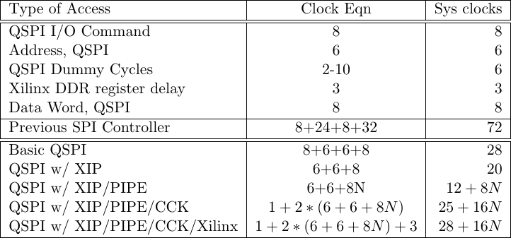 |
The top of this chart shows the number of clocks required for each part of a QSPI interaction. The basic transaction costs 8 clocks for the command word, followed by another 6 clocks to send 24-bits of address 4-bits at a time. After this point, the flash chip might require between 1 and 10 “dummy cycles”. This is an annoying requirement necessary to support Micron flash chips. Winbond and Spansion flash chips have a fixed number of dummy cycles: six–so we’ll use that going forward for our calculations. Following the dummy cycles, it takes 8 clocks to transfer one 32-bit word of information.
These are the numbers we’re dealing with.
Now for the controller options. Our last controller, operating in
SPI mode
alone, took 64 clock cycles to transfer a word. Switching to
Quad-SPI
alone brings us down to 28 cycles. Using the eXecute In Place mode allows
us to then skip the eight clocks of the
QSPI
I/O command, bringing our access time down another 8 cycles to 20 cycles. The
next request, however, will require another 20 cycles. On the other hand, if
we can string multiple requests for sequential addresses together into the
same request, using the pipelined mode of the
bus,
we can drop our access time from 20N clocks for N values down to 12+8N
clock cycles.
This is about as fast as a QSPI controller will get.
If you have to use the CCK port of a Xilinx
FPGA,
you’re clock rate will be
slowed down by at least 2x. I placed another clock in the chart above, to
allow the SCK to go low after the CS_n line becomes active. Then, if you are
using the registered Xilinx
DDR primitives,
you’ll be required to slow down another three clocks.
The “Universal” QSPI flash
core
can therefore provide performance somewhere between
12+8N clocks and 28+16N clocks per word, depending upon how it is set up,
how your board is designed, and the
flash
chip on that board.
Timing control loop
Let’s start out with our timing control, because the timing control signals are going to be pervasive throughout the rest of the core.
 |
In our highest speed configuration, we’re going to want to handle an SCK
signal equal to our controllers clock rate. Such a signal might generate
an output looking like Fig. 11 on the right. In this figure, the w_qspi_sck
control signal is being used to control the final o_qspi_sck output. (I’ll
also confess, these are top-level signal names. Within
the core,
I’ve used o_qspi_sck to reflect the signal shown at the right labeled
w_qspi_sck. In the non-ODDR modes, there’s no difference between these
two signals, only in the ODDR mode.)
Of course, we’ll want to be able to slow this clock down as well, so let’s create several signals from a basic clock divider circuit that we can use to control our logic below in the presence of a slower clock. These extra signals are shown in Fig. 12 below.
 |
The CS_n and SCK signals are part of the basic
QSPI
protocol. If CS_n
is inactive (high), then the other
SPI
signals, primarily clock and data, are allowed to be anything so that they
can be multiplexed together in order to control several chips. The SCK
signal controls the basic data transfer, and so we’ll focus on making sure
the SPI
data values only ever change when SCK falls.
The other clock control signals are:
-
ckstb: True when it’s time to move to the next set of output values.In a DDR output mode, this will be true on every cycle during a transaction. If we are dividing the clock by two, this will be true every other cycle.
-
ckneg: True when it’s time to set theSCKsignal lowSince we’ll only set
SCKlow at the beginning of a cycle, this signal is just a pseudonym for theckstbsignal above. -
ckpos: True when it’s time to set theSCKsignal highThis will take place mid-cycle.
Of course, if we are in a DDR output mode, that is with
SCKtoggling at the system clock rate, then this doesn’t nearly have as much meaning, so we’ll leave it high. -
ckpre: Some of the logic below will require an extra clock cycle to prepare for the next transition. This is the purpose ofckpre. It is designed so as to be true on the clock cycle prior tockstb.
The code within this section is parameterized by several pieces. The first is
the clock division parameter, OPT_CLKDIV. We’ll use this to control a clock
divider in a moment. The second parameter, really a localparam, is the
OPT_DDR parameter. We’ll set this any time OPT_CLKDIV == 0, and use
it to indicate that we are driving the SCK line at our full system clock rate,
using an ODDR output primitive.
localparam [0:0] OPT_ODDR = (OPT_CLKDIV == 0);In the case where OPT_ODDR is true, there’s only ever one clock per
SCK cycle. Hence, we’ll set all of these values true on every clock cycle.
	generate if (OPT_ODDR)
	begin

		always @(*)
		begin
			ckstb = 1'b1;
			ckpos = 1'b1;
			ckneg = 1'b1;
			ckpre = 1'b1;
		end
If we are dividing our clock by two, such as in order to use a CCK port
through a STARTUPE2 primitive,
then we’ll set OPT_CLKDIV to 1. We’ll also need to toggle these
signals–but only while the port is active. That way we can respond
to a request no matter what phase of the counter we are in.
	end else if (OPT_CLKDIV == 1)
	begin : CKSTB_ONE

		reg	clk_counter;

		initial	clk_counter = 1'b1;
		always @(posedge i_clk)
		if (i_reset)
			clk_counter <= 1'b1;
		else if (clk_counter != 0)
			clk_counter <= 1'b0;
		else if (bus_request)
			clk_counter <= (pipe_req);
		else if ((maintenance)||(!o_qspi_cs_n && o_wb_stall))
			clk_counter <= 1'b1;

		always @(*)
		begin
			ckpre = (clk_counter == 1);
			ckstb = (clk_counter == 0);
			ckpos = (clk_counter == 1);
			ckneg = (clk_counter == 0);
		end
For the sake of brevity, I’m going to skip the discussion of what it takes to divide the clock down slower then a factor of two. Fig. 12 above should show you what these signals need to look like in that case.
Before leaving this section, I’d like to draw your attention to the presence
of the three generate blocks for this timing: one for OPT_ODDR when the clock
divider is set to zero, one for when the clock divisions is set to one, and one
more for all other cases. That means that, when we get to
formally verifying
this core,
we’ll have to make certain that our formal
verification
work gets applied to each of these three blocks separately.
Reading a word
Now that we have the clock divider out of the way, we can turn our attention to the fun part: building the actual flash controller logic.
If you ever find yourself needing to build your own controller, whether it be a SPI, flash, SDRAM or whatever protocol, the way to do it is usually straight forward: Find the specification sheet for the device you wish to interact with, search through the sheet for the timing diagram illustrating the interaction or interactions you wish to implement, and then build a state machine whose trace matches that diagram.
Building a flash controller is no different.
In this case, we’ll be implementing the QUAD I/O READ function. If you look this function up in the data sheet for your device, you’ll find two sets of protocols. The first describes how to get into the QUAD I/O XIP mode. The second I/O function shows a timing diagram describing the QUAD I/O XIP mode we’ll be using.
For example, here’s what the timing diagram looks like for a Spansion device.
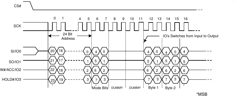 |
Here’s another one describing how our operation needs to work for a Winbond device.
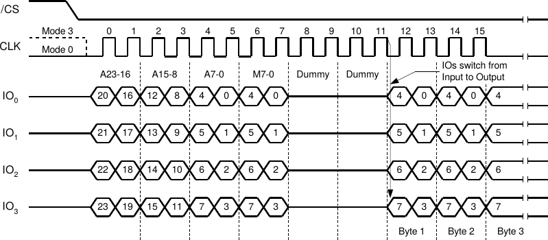 |
The data sheet for the Micron flash that I have doesn’t show the Quad I/O read from XIP mode, but it does show the Quad I/O read starting with the 8-bit command.
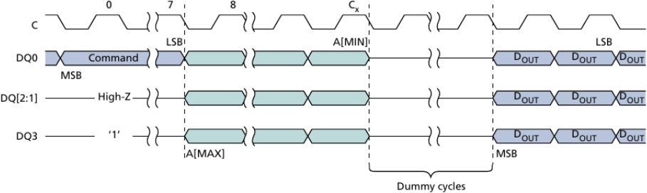 |
We’ll need to use this mode to get into the XIP mode, but more on that in a bit. For now, let’s just assume we are in the XIP mode where we can start immediately by sending the address to the flash device.
In all cases, we’ll need to go through several steps, and we’ll need to
control the chip select (negative logic), o_qspi_cs_n, the
SPI clock signal
sometimes called SCK, o_qspi_sck, and the four outgoing data wires,
o_qspi_dat. Since these wires will eventually be bi-directional at the top
level, we’ll use a third signal, o_qspi_mod, to control the final I/O driver.
We’ll also need to read the data lines from the
device, i_qspi_dat, once it starts returning information to us.
That means that we’ll need to support 3-I/O modes using o_qspi_mod:
-
NORMAL_SPI = 2'b00:DAT[0]is an output,DAT[1]is an input, andDAT[3:2]are both set high. -
QUAD_WRITE = 2'b10: All data wires,DAT[3:0], are outputs of our FPGA. -
QUAD_READ = 2'b11: All data wires,DAT[3:0], are inputs into our FPGA.
	localparam [1:0]	NORMAL_SPI = 	2'b00;
	localparam [1:0]	QUAD_WRITE = 	2'b10;
	localparam [1:0]	QUAD_READ = 	2'b11;
How the design interacts with the devices I/O controllers is typically beyond the scope of any of my QSPI flash designs, although it is required to actually implement them within any hardware. At one time, I would specify specific I/O connections in the toplevel:
	assign io_qspi_dat[0] = (w_qspi_mod[0]) ? w_qspi_dat[0] : 1'bz;
	assign io_qspi_dat[1] = (w_qspi_mod==2'b10) ? w_qspi_dat[1] : 1'bz;
	assign io_qspi_dat[3:2] = (w_qspi_mod == 2'b11) ? 1'bz
				: (w_qspi_mod == 2'b10) ? w_qspi_dat[3:2]
				: 2'b11;
I’ve stopped setting my I/O pins in this manner, however.
The primary reason for this is that Arachne-PNR would never guarantee that the placement of this final piece of combinatorial logic would be anywhere near the pin. As a result, I’ve now counseled several individuals who have declared Yosys broken when their design gets sufficiently large that the I/O logic no longer gets placed adjacent to their pins.
While I’m told that this is fixed in
NextPNR, I haven’t (yet) taken the time
to go back and verify this. Instead, I’ve gotten used to configuring the
vendor specific I/O buffers to handle this. Further, since I’m already using
one for the ODDR SCK pin, it makes sense to use the same thing for all of the
pins–if for no other reason than to keep the timing matching throughout the
design.
Hence our design will need to control o_qspi_cs_n, o_qspi_sck,
and o_qspi_dat[3:0]. We’ll also control an intermediate value, o_qspi_mod
to tell an external I/O controller how we want the I/O handled. Similarly,
we’ll be reading from i_qspi_dat[3:0], the data lines that come from that
external I/O controller.
So let’s go back to how this controller will need to control these various wires.
The basic logic is that upon any bus request, we will need to work our way through a sequence of steps.
Just like with the state machine examples in my tutorial, I often find that using a counter to control the steps in the timing diagram feels the most natural–especially in a particularly long sequence such as this one. In this case, the counter idles at zero, and starts counting down immediately following a bus request. Once the counter reaches zero, the interface will return to idle and we should be producing our Wishbone (WB) acknowledgment.
You can see this counter, clk_ctr, and how it relates to our design in Fig. 16
below.
 |
This one counter controls everything, so let’s walk through the steps of how it works.
Our logic starts with a bus request,
assign bus_request = (i_wb_stb)&&(!o_wb_stall)&&(!i_wb_we);where we set our counter to 14 plus the number of dummy cycles,
NDUMMY. This number of dummy cycles also includes two cycles for
the mode bits, 8'ha.
	initial	clk_ctr = 0;
	always @(posedge i_clk)
	if (i_reset)
		clk_ctr <= 0;
	else if (bus_request)
		clk_ctr <= 5'd14 + NDUMMY + (OPT_ODDR ? 0:1);
Note, above, that if we are not running in OPT_ODDR mode, that mode that
runs the SCK at the system clock speed, then we take an extra step to lower
the clock line after activating the chip select. This will cost us one extra
clock, and so this first value of clk_ctr depends upon OPT_ODDR in addition
to NDUMMY.
 |
|
On the other hand, if we are running in ODDR mode, then it feels like a waste
to spend a whole cycle to lower SCK, so both CS_n and SCK will drop
together, as shown in Fig. 18 on the right.
Once set, then on any following step during this operation, we’ll decrement our counter until it reaches zero.
	else if ((ckstb)&&(|clk_ctr))
		clk_ctr <= clk_ctr - 1'b1;
Once it reaches zero, we are idle.
Now that we have this counter, we can hang all of the rest of our logic upon it.
For example, here’s the outgoing chip select bit. Remember, this is an active low bit. On any bus request, we’ll clear this bit.
	initial	o_qspi_cs_n = 1'b1;
	always @(posedge i_clk)
	if (i_reset)
		o_qspi_cs_n <= 1'b1;
	else if (bus_request)
		o_qspi_cs_n <= 1'b0;
Then at the end of every clock interval, we’ll check the clk_ctr to
know if this operation is over. Once the counter gets to one, we’ll set
o_qspi_cs_n again to indicate the end of the operation on the next cycle.
	else if (ckstb)
		o_qspi_cs_n <= (clk_ctr <= 1);
The SPI
clock is a bit more difficult, particularly because of our requirements
creep. If we are running in OPT_ODDR mode, where the outgoing SCK is
determined by an ODDR I/O primitive, then we’ll output a 1'b1 anytime
we want the clock to toggle.
	initial	o_qspi_sck = (!OPT_ODDR);
	always @(posedge i_clk)
	if (i_reset)
		o_qspi_sck <= (!OPT_ODDR);
	else if (bus_request)
		o_qspi_sck <= 1'b1;
	else if (OPT_ODDR)
	begin
		if (clk_ctr[4:0] > 5'd1)
			o_qspi_sck <= 1'b1;
		else
			o_qspi_sck <= 1'b0;
If you look closely, you might argue that this o_qspi_sck signal is
identical to the o_qspi_cs_n signal. At this most basic mode, and only if
OPT_ODDR is true, then these two signals could share the same logic.
I should point out that I ended up using parameters quite extensively in this
core. OPT_ODDR isn’t the only one. I did this for reasons of code
optimization. By using OPT_ODDR, the synthesis tool can quickly recognize
the if (OPT_ODDR) statement, and that the else following will never get
used. Hence, the synthesis tool will remove the rest of this nested if.
Similarly, if OPT_ODDR isn’t true, this part of the if will get removed
and not count against the logic used by this core.
If OPT_ODDR isn’t true then things get just a little more interesting.
As per the SPI protocol we are following, the clock idles at 1'b1 over the
wire, and so it idles at 1'b1 in non-ODDR mode where we
are directly controlling the over-the-wire interface. On the other hand, if
we are running in OPT_ODDR mode, we are only controlling whether the clock
toggles. Hence in OPT_ODDR mode, the clock pin idles at 1'b0.
(See Figs. 11 and 12 for clarification)
Now, if the clock is low, and ckpos tells us that it is time to raise it,
then set it high. This will occur in the middle of our
state machine
interval, and only if OPT_ODDR isn’t set.
	end else if ((ckpos)&&(!o_qspi_sck))
	begin
		o_qspi_sck <= 1'b1;
Finally, if our clock divider tells us it is time to lower the clock, that
is if ckneg is true, then lower the o_qspi_sck output–but only if our
SPI cycle isn’t finished. Notice the check here, as above, for whether are or
are not still within any I/O operation.
	end else if ((ckneg)&&(o_qspi_sck)) begin

		if (clk_ctr[4:0] > 5'd1)
			o_qspi_sck <= 1'b0;
		else
			o_qspi_sck <= 1'b1;
	end
Now that we’ve set the chip select and the clock, we can turn our attention
to the data bits. These get set on any bus request, and
then shifted at the end of every clock interval. Ideally, that would mean
we’d set this anytime i_wb_stb && !o_wb_stall. However, I’ve become somewhat
of a stickler for low-logic solutions, and the reality is that these bits are
don’t cares if !i_wb_stb && !o_wb_stall, so I just check for !o_wb_stall
here.
	initial	data_pipe = 0;
	always @(posedge i_clk)
	if (!o_wb_stall)
	begin
		// Set the high bits to zero initially
		data_pipe <= 0;

		data_pipe[8+LGFLASHSZ-1:0] <= {
				i_wb_addr, 2'b00, 4'ha, 4'h0 };
	end else if (ckstb)
		data_pipe <= { data_pipe[(32+4*((OPT_ODDR ? 0:1)-1))-1:0], 4'h0 };

	assign	o_qspi_dat = data_pipe[28+4*(OPT_ODDR ? 0:1) +: 4];
Perhaps if I were interested in building a lower power design, I’d want to eliminate any extraneously toggling data.
	initial	data_pipe = 0;
	always @(posedge i_clk)
	if (!o_wb_stall)
	begin
		data_pipe <= 0;
		if (i_wb_stb)
			data_pipe[8+LGFLASHSZ-1:0] <= {
				i_wb_addr, 2'b00, 4'ha, 4'h0 };
	// ...
But low-power isn’t my current goal.
For now, you can see how LGFLASHSZ address bits get set, the lower two
address bits get cleared (since we are responding to a 32-bit data
bus request), and the 4'ha
mode bits get set. These mode bits will help to guarantee that we don’t leave
XIP mode once we’ve gotten into it.
Sure, the entire QSPI read operation is longer than this, but there’s never a time when we’ll need to output more valid bits than this. Indeed, after these bits get sent, the controller will switch the I/O lines from output to input modes, so again there’s no reason to care about these bits after the output duration of this operation ends.
The last QSPI I/O interface item that needs to be controlled is the I/O mode, to be used in determining which bits are set to outputs and which bits to inputs in the external I/O controller.
We’ll start in NORMAL_SPI mode, and then transition on a bus request
to QUAD_WRITE mode in order to send the address of the data we wish to read.
	initial	o_qspi_mod =  NORMAL_SPI;
	always @(posedge i_clk)
	if (i_reset)
		o_qspi_mod <= NORMAL_SPI;
	else if (bus_request)
		o_qspi_mod <= QUAD_WRITE;
Once we get past the address and mode bits, we can then go into QUAD_READ
mode to read our data.
	else if ((ckstb)&&(clk_ctr <= 5'd9))
		o_qspi_mod <= QUAD_READ;
That’s the logic necessary to control a read.
But what about the rest of our bus logic? While all of this is going on, we need to be doing a couple of things. First, the bus must be stalled. Second, we need to be collecting data from the QSPI data lines to return to the bus. Finally, once the operation completes, we need to acknowledge the bus request, signaling that the data we’ve collected is now valid.
Let’s start with the stall signal. On any bus request, we’ll set the stall signal high since it will be many cycles before we can respond to another bus request.
	initial	o_wb_stall = 1'b1;
	always @(posedge i_clk)
	if (i_reset)
		o_wb_stall <= 1'b1;
	else if (bus_request)
		o_wb_stall <= 1'b1;
Then, at the end of every clock interval, we’ll adjust the stall signal so that
it remains high until our operation is done. Once clk_ctr == 0, we’ll both
(potentially) acknowledge the request, and drop our stall signal.
	else if (ckstb)
	begin
		if (clk_ctr > 1)
			o_wb_stall <= 1'b1;
		else
			o_wb_stall <= 1'b0;
	end
We’ll come back to this in a bit and discuss how to handle the register delays
on our input wires, since that will force us to keep the o_wb_stall
line high even after our transaction has finished.
The Wishbone acknowledgement signal looks simple enough. Following the
clock cycle where clk_ctr==1, we’ll acknowledge this request.
	always @(posedge i_clk)
	if (i_reset)
		o_wb_ack <= 1'b0;
	else
		o_wb_ack <= (ckstb)&&(clk_ctr == 1);
Only … this is where we start to get in trouble with reality.
First, a formal proof
of this logic fails if the master drops the i_wb_cyc line before we have the
chance to set this acknowledgment. We can’t interrupt our
flash I/O cycle when this happens,
lest we fail to output the 0xa0 mode bits and the
flash chip get placed into a
state other than the XIP one. Therefore, we’ll need to keep track of
whether the bus master has dropped the i_wb_cyc line and then suppress any
acknowledgments if it had.
The pre_ack logic below keeps track of whether or not we are still
within the original
bus cycle.
	always @(posedge i_clk)
	if ((i_reset)||(!i_wb_cyc))
		pre_ack <= 1'b0;
	else if (bus_request)
		pre_ack <= 1'b1;
That way we can use it, within our calculation of the bus acknowledgment, to return a proper value.
	initial	o_wb_ack = 1'b0;
	always @(posedge i_clk)
	if (i_reset)
		o_wb_ack <= 1'b0;
	else if ((ckstb)&&(clk_ctr == 1))
		o_wb_ack <= (i_wb_cyc)&&(pre_ack);
This isn’t quite the last of our problems either. What if a user wants to write to our read-only memory? Such an operation is undefined, but we can’t allow the bus to stall waiting for the result of an unsupported operation. If I believed in bus errors, I might raise one here–and there are a lot of good reasons to do so. I chose instead to quietly acknowledge any write request without doing anything instead.
	else if ((i_wb_stb)&&(!o_wb_stall)&&(!bus_request))
		o_wb_ack <= 1'b1;
	else
		o_wb_ack <= 1'b0;
Our last step is to set and return our data value to the WB bus
That one’s easy, right? Anytime there’s a value to be read, shift it into our data register.
	always @(posedge i_clk)
	if (read_sck)
		o_wb_data <= { o_wb_data[27:0], i_qspi_dat };
But, when is there data to be shifted in? Here, I use a separate signal,
read_sck, to capture this logic. While I could have used ckstb, and
certainly did initially, I had to adjust this approach later to make certain
that o_wb_data never changes unless we are mid-operation with clk_ctr > 0
If we are in OPT_ODDR mode, the mode where SCK can toggle at the system
clock speed, then anytime the output clock is active, we should be reading
into our shift register.
	generate if (OPT_ODDR)
	begin : SCK_ACTUAL

		always @(*)
			read_sck = o_qspi_sck;
You can see the resulting waveform trace in Fig. 19 below.
 |
This would be catastrophic, though, if we only wanted to shift the data in
on every other clock. Hence, if we are dividing the clock by two, then
we want to read on the last clock of every clock cycle. One clock before
then, o_qspi_sck will be low.
	end else if (OPT_CLKDIV == 1)
	begin : SCK_ONE

		initial	read_sck = 1'b0;
		always @(posedge i_clk)
		if (i_reset)
			read_sck <= 1'b0;
		else
			read_sck <= (!o_qspi_sck)&&(clk_ctr > 0);
This extra logic is shown in the last line of the trace shown below in Fig. 20.
 |
Finally, if we are dividing by anything more than two, then we’ll register the
read_sck signal, and use the ckpre signal as our indication that we
need to sample on the next clock.
	end else begin : SCK_ANY

		initial	read_sck = 1'b0;
		always @(posedge i_clk)
		if (i_reset)
			read_sck <= 1'b0;
		else
			read_sck <= (o_qspi_sck)&&(ckpre)&&(clk_ctr > 0);

	end endgenerate
Again, this is shown in Fig. 21 below. Notice how ckpre is true one clock
before read_sck, as required to make this work. Notice also how the
clock goes through its negative cycle first, leaving the SCK positive
edge mid-interval.
 |
To verify that this logic works, I used one of those “poor man’s sequences” that I discussed earlier.
Why not use a regular SystemVerilog sequence? Well, I started out using the more traditional SVA sequences. However, ultimately it was the variable clock rate that made using SVA sequences impossible, and so I had to switch to the poor man’s sequence approach.
By a poor man’s sequence, I mean something like the following:
First, I define how long this operation will take in logical steps, not
clock steps. This
includes the first step, found only when OPT_ODDR is low, where the CS_n line
is low and SCK remains high, followed by the six clock intervals of
the address. This is then followed by a parameterizable number of dummy cycles,
and then our eight data read cycles. We can capture this total length with the
localparam, F_MEMDONE.
localparam F_MEMDONE = (OPT_ODDR ? 0:1) + 6 + NDUMMY + 8;We can then define a sequence vector of this many states, plus one more for the acknowledgment cycle, with the meaning that if any of the bits in this vector is a one, then we are in that state.
reg [F_MEMDONE:0] f_memread;The logic to control this sequence is actually fairly simple. On a reset, the sequence is cleared.
	initial	f_memread = 0;
	always @(posedge i_clk)
	if (i_reset)
		f_memread <= 0;
Otherwise, we advance the sequence at the end of every SCK clock period.
	else begin
		if (ckstb)
			f_memread <= { f_memread[F_MEMDONE-1:0], 1'b0 };
There’s one problem with only stepping the sequence at the end of every
SCK clock interval: what happens to the acknowledgment? o_wb_ack can only
be high for one clock cycle, not for as many cycles as there are in an
extended SCK clock interval. Therefore, we’ll need to clear the upper bit
if our clocking is extended at all.
		else
			f_memread[F_MEMDONE] <= 1'b0;
The last step is to start the sequence. We’ll start it on any bus
request. Well, almost. For reasons we’ll get into later we’ll start this
only on a bus request where the CS_n line is idle (high).
		if (bus_request && o_qspi_cs_n)
			f_memread[0] <= 1'b1;
	end
From here, we’ll shift this left one step per every state transition. Fig. 35 below shows an example of this, but only after adding in several more features, so let’s work our way up to that point.
Now we can make assertions about what’s supposed to happen in each step.
For example, we want to make certain o_qspi_sck is high during any OPT_ODDR
read operation.
	always @(posedge i_clk)
	if ((OPT_ODDR)&&(|f_memread[F_MEMDONE-1:0]))
		assert(o_qspi_sck);
We might also wish to assert that we start out this sequence in QUAD_WRITE
mode, and end it in QUAD_READ mode. There’s a couple steps in the middle
where our I/O mode doesn’t matter, but otherwise this fully constraints our
I/O modes.
	always @(posedge i_clk)
	if (|f_memread[6+(OPT_ODDR ? 0:1):0])
		assert(o_qspi_mod == QUAD_WRITE);
	else if (|f_memread[(OPT_ODDR ? 0:1)+7 +: NDUMMY])
	begin end
	else if (|f_memread)
		assert(o_qspi_mod == QUAD_READ);
In a moment, we’ll need a copy of what was read from the i_qspi_dat set of
input pins in order to verify that we received the right values. So let’s
create a second copy of the incoming data for that check.
	always @(posedge i_clk)
	if (ckpos && o_qspi_mod == QUAD_READ)
		f_past_data <= { f_past_data[28:0], i_qspi_dat[3:0] };
	end
Next, let’s examine those first six clocks. These are the ones where we need to be outputting the address we were given from the bus. The first step to this check is making sure we have a copy of the last requested address to check against.
	always @(posedge i_clk)
	if (bus_request)
	begin
		// Make sure all of the bits are set
		fv_addr <= 0;
		// Now set as many bits as we have address bits
		fv_addr[AW-1:0] <= i_wb_addr;
	end
We can now use this to compare against what we are presenting across the port.
For example, during our first time interval, we’ll want to output address
bits 21:18.
	always @(posedge i_clk)
	if (|f_memread[(OPT_ODDR ? 0:1) +: 7])
	begin
		// 6 nibbles of address, one nibble of mode
		if (f_memread[(OPT_ODDR ? 0:1)])
			assert(o_qspi_dat== fv_addr[21:18]);
Don’t let the OPT_ODDR scare you in this expression. This just references
the extra clock cycle used in the slow clock mode before lowering the SCK
line. During that cycle, output data values are don’t cares, so we don’t
check them here. However, if we are running in the faster mode, then we
don’t take an extra cycle–hence the reason for checking whether or not
OPT_ODDR is set here or not.
Here are the rest of the checks for the rest of the address intervals.
		if (f_memread[1+(OPT_ODDR ? 0:1)])
			assert(o_qspi_dat== fv_addr[17:14]);
		if (f_memread[2+(OPT_ODDR ? 0:1)])
			assert(o_qspi_dat== fv_addr[13:10]);
		if (f_memread[3+(OPT_ODDR ? 0:1)])
			assert(o_qspi_dat== fv_addr[ 9: 6]);
		if (f_memread[4+(OPT_ODDR ? 0:1)])
			assert(o_qspi_dat== fv_addr[ 5: 2]);
Don’t forget that, because we are addressing the flash with 32-bit word addresses, that the bottom two of twenty-four bits are necessarily zero.
		if (f_memread[5+(OPT_ODDR ? 0:1)])
			assert(o_qspi_dat=={ fv_addr[1:0],2'b00 });
Or, likewise, if we want to stay in XIP mode (and we do), that we have to
output a 4'ha following the address.
		if (f_memread[6+(OPT_ODDR ? 0:1)])
			assert(o_qspi_dat == 4'ha);
	end
Now let’s turn our attention to the returned result.
In OPT_ODDR mode, we get a result every clock tick. In this case,
the $past() function is ideal for checking if we are returning the right
values.
	always @(posedge i_clk)
	if (OPT_ODDR)
	begin
		if (f_memread[F_MEMDONE])
		begin
			assert(o_wb_data[31:28] == $past(i_qspi_dat,8));
			assert(o_wb_data[27:24] == $past(i_qspi_dat,7));
			assert(o_wb_data[23:20] == $past(i_qspi_dat,6));
			assert(o_wb_data[19:16] == $past(i_qspi_dat,5));
			assert(o_wb_data[15:12] == $past(i_qspi_dat,4));
			assert(o_wb_data[11: 8] == $past(i_qspi_dat,3));
			assert(o_wb_data[ 7: 4] == $past(i_qspi_dat,2));
			assert(o_wb_data[ 3: 0] == $past(i_qspi_dat,1));
On the other hand, if we haven’t yet reached the end of the sequence, then both the stall signal should be high and the acknowledgment signal should be low.
		end else if (|f_memread)
		begin
			assert(o_wb_stall);
			assert(!o_wb_ack);
		end
If we are running in a slower clock mode, then $past() won’t work for us.
Instead, we can use the copy we just made of the incoming data to prove
that we received the right value.
	end else if (f_memread[F_MEMDONE])
		assert((!o_wb_ack)||(o_wb_data == f_past_data[31:0]));
The rest of this logic should match the logic above.
	else if (|f_memread)
	begin
		assert(o_wb_stall);
		assert(!o_wb_ack);
	end
We also want to make certain that, on the very last clock tick, the counter has properly returned to zero.
	always @(posedge i_clk)
	if (f_memread[F_MEMDONE])
		assert(clk_ctr == 0);
We’ll use one final assertion to double check that f_memread only ever has
one value active at any given time.
	generate for(k=0; k<F_MEMACK-1; k=k+1)
	begin : ONEHOT_MEMREAD
		always @(*)
		if (f_memread[k])
			assert((f_memread ^ (1<<k)) == 0);
	end endgenerate
Finally, just to get some assurance that this actually works, we’ll add a
cover() statement to check that, yes, we truly can perform this operation.
	always @(posedge i_clk)
		cover(o_wb_ack && f_memread[F_MEMACK]);
We now have a basic, functioning, QSPI flash controller. Or do we? So far, I’ve only presented how to handle requests once we’ve already gotten into this special XIP mode. We’ll have to come back to the question of how to get into this mode in the first place still. Similarly, we haven’t discussed how to send or receive arbitrary commands yet, or how to handle I/O delays. Let’s push those topics off for a bit longer, and look at how to read a second word without needing to go through the address cycle again.
Reading another word
 |
With the logic above, we can now read a word from our flash chip. We can do this at the system clock rate, or any arbitrary division of it. In this section, let’s instead focus on what it takes to read data from the flash using the pipelined features of the Wishbone bus.
While you might wish to call this a burst bus mode, unlike other burst modes that I’ve worked with (WB, AXI, etc), this one doesn’t carry a burst length parameter, burst size, or even address increment information. For this reason, I often call this a pipelined mode rather than a burst mode, even though there are some obvious similarities between the two. As a result, you’ll find I often describe these as “pipe” or “piped” requests.
Within my design, this pipelined mode is controlled by the OPT_PIPE parameter.
Further, unlike many bus burst
modes, these piped requests are controlled on a beat by beat basis in the
master. There’s no pre-announcement of the number of values to be read, such
as in the AXI master specification
or in the Wishbone burst modes from the B3
specification that I’ve
carefully chosen not to
implement. Instead, we’ll
need to determine on a beat by beat basis if the next read request continues the
burst, or if we need to raise o_qspi_cs_n and start over with a new
QSPI
transaction.
Here you can see the definition of the OPT_PIPE parameter controlling whether
or not we support this mode in the first place.
	// OPT_PIPE makes it possible to string multiple requests together,
	// with no intervening need to shutdown the QSPI connection and send a
	// new address
	parameter [0:0]	OPT_PIPE    = 1'b1;
If this parameter is set, the controller will respond to requests for subsequent
addresses. Hence, if you request a read from address A, and then while the
controller is busy making that happen you request a second read from address
A+1 (i.e. one word, or 32-bits later), then the controller should recognize
and honor this request before closing up the interface.
Sadly, that means we’re going to need to go back over a lot of our logic above and adjust it to make these subsequent reads possible.
The first step, though, is a bit of complicated logic determining if a subsequent read is even pending that would extend our burst access in the first place.
	generate if (OPT_PIPE)
	begin : OPT_PIPE_BLOCK
		reg	r_pipe_req;
		wire	w_pipe_condition;

		reg	[(AW-1):0]	next_addr;
An important part of this check is to know if a bus request is pending for
the next address. The first step of that logic is to calculate what that
next address, or next_addr, will be. In particular, this address is defined
as one more than the last address accepted. Hence, anytime !o_wb_stall, we
can create a copy of the incoming address plus one. (Notice we dropped the
check for i_wb_stb again.) Following requests for this next_addr
will then be honored without closing the interface.
		always  @(posedge i_clk)
		if (!o_wb_stall)
			next_addr <= i_wb_addr + 1'b1;
This will capture the next_addr from not only the beginning of our first
request, but will also update it at the beginning of any subsequent address
as well, since the logic above, based upon the !o_wb_stall signal alone,
doesn’t care which of the two it is responding to.
A pipe request requires several things that all need to be true.
First, this has to be part of the last transaction. Remember how we used
pre_ack to keep track of whether the last transaction was aborted?
Here, pre_ack must be true–indicating that the last request was never
aborted. Second, there must be an outstanding request, so i_wb_stb must
be true as well. The new request must also be a read request, so !i_wb_we.
Further, it must be a request while we are already busy, and so the CS_n pin
must be active so !o_qspi_cs_n. The clock counter must be greater than
zero, and the outstanding request must be for the next address.
		assign	w_pipe_condition = (i_wb_stb)&&(!i_wb_we)&&(pre_ack)
				&&(!o_qspi_cs_n)
				&&(|clk_ctr[2:0])
				&&(next_addr == i_wb_addr);
This all makes sure that we are not only receiving a next address read request, but also that we are getting that request while we are still reading from the last address.
Since that’s a lot of logic, we’ll register it to keep it from slowing down the rest of the core.
		initial	r_pipe_req = 1'b0;
		always @(posedge i_clk)
		if ((clk_ctr == 1)&&(ckstb))
			r_pipe_req <= 1'b0;
		else
			r_pipe_req <= w_pipe_condition;

		assign	pipe_req = r_pipe_req;
Of course, if we aren’t supporting burst reads, then this value needs to be kept at zero–so the synthesizer can optimize away any unused logic.
	end else begin
		assign	pipe_req = 1'b0;
	end endgenerate
Registering all this logic is going to change our timing diagram somewhat, as shown in Fig. 23 below.
 |
Notice from the figure that the logic recognizing a pipelined request needs
to first notice the request when clk_ctr == 3. Then pipe_req gets set
one clock later, when clk_ctr == 2, and so the o_wb_stall line gets
dropped when clk_ctr == 1. This is all set up so that clk_ctr can then
jump back from clk_ctr==1 to clk_ctr == 8 to start the second read.
The formal tools,
however, discovered the error in this basic set up. If
I ever take more than one clock cycle per SCK, then it might be that
clk_ctr == 1 for multiple cycles before o_wb_stall needs to be lowered.
Thanks to the formal
tools,
I think I found all of the missing logic tests.
All that’s left then is to patch this into our prior logic. The biggest
changes will be to our counter, clk_ctr, and our stall signal, o_wb_stall.
Neither the o_qspi_cs_n logic nor the o_qspi_sck logic needs to change,
since both of these are already set appropriately on any bus request.
Let’s start by updating clk_ctr. Before, on a read request, we set the
clk_ctr to 14+NDUMMY+(!OPT_ODDR). Now, if pipe_req and bus_request are
true, we’ll need to set it to 8 just before the operation ends.
	// We start out as before
	initial	clk_ctr = 0;
	always @(posedge i_clk)
	if (i_reset)
		clk_ctr <= 0;
	else if ((bus_request)&&(!pipe_req))
		// Notice that this is only appropriate for
		// regular bus reads, and so the check for
		// !pipe_req
		clk_ctr <= 5'd14 + NDUMMY + (OPT_ODDR ? 0:1);
	else if (bus_request) // && pipe_req
		// Otherwise, if this is a piped read, we'll
		// reset the counter back to eight.
		clk_ctr <= 5'd8;
	else if ((ckstb)&&(|clk_ctr))
		// The rest is as it was before
		clk_ctr <= clk_ctr - 1'b1;
At first, updating the stall signal is easy. We still raise the stall signal on a bus request, regardless of whether or not its a piped (burst) request.
	initial	o_wb_stall = 1'b1;
	always @(posedge i_clk)
	if (i_reset)
		o_wb_stall <= 1'b1;
	else if (bus_request)
		o_wb_stall <= 1'b1;
Where things start to get difficult is when determining when to drop the stall line in order to accept this transaction.
It turns out that there’s two separate pieces of logic required. First, if
we are in OPT_ODDR mode and hence running at the system clock, then we’ll
need to drop o_wb_stall when clk_ctr == 2 so that o_wb_stall will be low
when clk_ctr == 1 as shown in Fig. 23 above.
	else if (ckstb || clk_ctr == 0)
	begin
		if (ckpre &&(i_wb_stb)&&(pipe_req)&&(clk_ctr == 5'd2))
			o_wb_stall <= 1'b0;
		else if (clk_ctr > 1)
			o_wb_stall <= 1'b1;
		else
			o_wb_stall <= 1'b0;
Remember, we can’t make a mistake here, and timing is critical. Once mistake,
where o_wb_stall is low for one too many clock cycles, and we might
accidentally accept an extra request that we have no intention of processing.
On the other hand, if we are running slower than our clock speed, then we’ll
need to drop the stall signal while clk_ctr == 1 as discussed above.
This needs to be done one clock before ckstb when all of our states change,
and so we use the ckpre signal for that purpose. Notice that, if OPT_ODDR
is true, ckstb in the above condition will always be true, so this next bit
of logic will get ignored.
	end else if (ckpre && (i_wb_stb)&&(pipe_req)&&(clk_ctr == 5'd1))
		o_wb_stall <= 1'b0;
Again, if you get confused by this logic at all, refer back to Figs. 11 or 12 above.
Verifying the piped reads follows much of the same logic as the original memory read verification: we use a poor man’s sequence. This sequence is only ever nine steps in length, since all the variable length stuff was handled above. These eight states represent the eight new steps on the QSPI bus, as well as a final one to return an Wishbone acknowledgment.
	localparam	F_PIPEDONE = 8;
	// ...
	reg	[F_PIPEDONE:0]	f_piperead;
Now we can define a shift register with eight states (plus one for the acknowledgment), and step through it every time a clock period completes. This should look very similar to the shift register associated with the poor man’s sequence for reading in the first place.
	initial f_piperead = 0;
	always @(posedge i_clk)
	if ((i_reset)||(!OPT_PIPE))
		f_piperead <= 0;
	else if (ckstb) begin
		// Shift left, to advance the states in our sequence
		f_piperead <= { f_piperead[F_PIPEDONE-1:0], 1'b0 };

		// Likewise, we start this sequence on a bus request when we
		// are already running
		f_piperead[0] <= (bus_request && !o_qspi_cs_n);
Of course, if the states last longer than a single clock, then we’ll need to make certain that any bus acknowledgments still don’t last any longer than a single clock.
	end else if (!OPT_ODDR)
		f_piperead[F_PIPEDONE] <= 1'b0;
Using this state sequence vector, we can now make assertions about this second part of our state machine. For example, on that last beat of the sequence, either the data is right, or the acknowledgments must be low–in which case we don’t care what’s in the data.
	always @(posedge i_clk)
	if (f_piperead[F_PIPEDONE])
		assert((!o_wb_ack)||(o_wb_data == f_past_data));
Now let’s look at the rest of the steps in the sequence. Prior to our
acknowledgment, we should be stalled until the end of the SCK clock cycle.
	else if (|f_piperead)
	begin
		if (!ckstb)
			assert(o_wb_stall);
Once we hit the end of the SCK clock cycle, we should still be stalled for all
stages except the one before we are done. That one exception is the stage,
shown in Fig. 23 above when clk_ctr == 1, where we might possibly accept
another request.
		else if (!f_piperead[F_PIPEDONE-1])
			assert(o_wb_stall);
Finally, unless we are acknowledging the last memory cycle, the acknowledgment line must also be low. (Remember, we checked for our own acknowledgment cycle earlier in this cascaded if statement.)
		if (!f_memread[F_MEMDONE])
			assert(!o_wb_ack);
	end
One last assertion is necessary to tie our f_piperead vector to the clock
counter. On the very last cycle of f_piperead, the clk_ctr should be at
zero, unless we are extending into an additional burst read following this
one in which case clk_ctr should be eight.
	always @(posedge i_clk)
	if (f_piperead[F_PIPEDONE])
		assert(clk_ctr == 0 || clk_ctr == F_PIPEDONE);
For all other cycles, the clk_ctr should specify which of the f_piperead
bits is on.
	else if (|f_piperead)
		assert(f_piperead[F_PIPEDONE-clk_ctr]);
As one final step to know that our core truly passes, we’ll add a cover statement to cover the acknowledgment from one of these pipe reads.
	generate if (OPT_PIPE)
	begin
		always @(posedge i_clk)
			cover(o_wb_ack && f_piperead[F_PIPEDONE]);
	end endgenerate
Now, when we run SymbiYosys in cover mode, we’ll get a trace that we can examine assuring us that our design truly did what we were expecting.
The Startup Sequence
 |
Our core now possesses all of the functionality necessary to read from the flash, just not any of the functionality necessary to get into the Quad I/O XIP read mode that all of our reads will start from. Once there, we can read at full speed (or slower) upon any request, and we can continue that read request as long as the master continues issuing subsequent read requests. Getting into this mode in the first place will be the topic of this section. Well, that and how to patch the logic for such a startup sequence into the logic we’ve already written above.
Before getting into the details, I should note that I’ve built more than one of these startup scripts before. Sadly, they all end up being very device dependent, often because different Flash devices support different reset commands, and some need special instructions to set chip specific configuration registers. Hence, while the previous two sections are all (fairly) device independent, and while they all apply to any flash device that supports the Quad I/O XIP read mode, things become quite device dependent in this section.
When I built my first startup script,
I built my startup sequence from a giant counter. After letting the
flash idle for a period of time,
following the Spansion
specification I was following for starting the
flash, I would then toggle the CS_n
line as a form of a reset sequence, and then issue a single read command.
Sometimes this required setting the Quad-SPI enable bit in the configuration
register.
This all worked until I tried using the Micron
flash chip. In that case, toggling
the CS_n line without toggling SCK wasn’t guaranteed to do anything useful.
Worse, before setting the Quad-SPI enable bit, you had to set the write enable bit. And, if that wasn’t
all, the Micron
flash chip
required up to 10-cycles between the address and the
data. Not only that, but that number of cycles is clock rate dependent. If
you didn’t run at 100MHz, you might be able to use fewer dummy cycles–making
the number of dummy cycles not only vendor but also clock rate dependent. If
that wasn’t enough, my 100 MHz flash
implementation required setting the drive strength, measured in Ohms, in order
to actually get up to 100MHz, and that requires setting the write enable bit
again.
So I rebuilt my flash driver in order to support this Micron flash chip as well as the others.
Because of the number of times I’ve ended up rebuilding this startup script, I chose to rebuild it this last time using an array of startup micro-commands rather than a counter driven script. While this might not be as low logic as I like, it will at least be easy enough to adjust from one flash device to the next.
This, therefore, is the one piece of our “Universal” flash
controller
that remains device dependent–not counting the number of dummy cycles,
the FPGA
dependent number of wait states on registered I/O, the device dependent
SCK rate, or ….
Here’s how our micro-control commands will be formatted.
 |
-
We’ll use one bit to select between a command to be send to the device, and some number of counts to wait idle before the next command. I call this the wait bit,
M_WAITBIT, within the code and marked it asSfor sleep in Fig. 25 above. If this bit is set, the other 10-bits of the command word will indicate the number of counts to remain idle with theCS_nline inactive (high). If the bit is not set, theCS_nline will be made active (low). Indeed, this sleep mode is currently the only way to setCS_ninactive between commands. -
The next two bits, shown as
Mabove, will select the mode the command will be in, whetherNORMAL_SPI,QUAD_WRITE, orQUAD_READ. -
The final 8-bits will record an 8-bit data byte to be sent to the device–in either high or low speed, or ignored in
QUAD_READmode.
I’ll admit, this is even my second version of this micro-code interface. My first version was a basic bit-banging microcode interface. I switched to the more complicated command interface when the bit-banging one started to become difficult to maintain. Now, with all of the commands specifying 8-bit byte values, the command script has become much easier to read and check by eye.
The good news is that we will barely need to adjust anything else in our design to make this startup script work once it comes time to integrate it.
The startup script begins with the array of instructions, each 11-bits long.
	localparam	M_LGADDR=5;
	//
	reg	[M_WAITBIT:0]	m_cmd_word	[0:(1<<M_LGADDR)-1];
These words are set within a giant initial block. In general, this block needs to start by placing the flash chip into a known state from which we can send an SPI command to enter the QSPI XIP read state,
	m_cmd_word[5'h08] = { 1'b0, NORMAL_SPI, 8'hff }; // Addr 1
	m_cmd_word[5'h09] = { 1'b0, NORMAL_SPI, 8'hff }; // Addr 2
	m_cmd_word[5'h0a] = { 1'b0, NORMAL_SPI, 8'hff }; // Addr 2
	// Idle, to raise the CS_n line
	m_cmd_word[5'h0b] = { 1'b1, 10'h3f };
and end with a Quad Read I/O command, 0xeb,
24-bits of address (I set these to zero in general), a mode command, 0xa0,
some number of dummy cycles as determined by your specification sheet, and
then reading one or two bytes for good measure.
	m_cmd_word[5'h14] = { 1'b0, NORMAL_SPI, 8'heb };
	// Addr #1
	m_cmd_word[5'h15] = { 1'b0, QUAD_WRITE, 8'h00 };
	// Addr #2
	m_cmd_word[5'h16] = { 1'b0, QUAD_WRITE, 8'h00 };
	// Addr #3
	m_cmd_word[5'h17] = { 1'b0, QUAD_WRITE, 8'h00 };
	// Mode byte
	m_cmd_word[5'h18] = { 1'b0, QUAD_WRITE, 8'ha0 };
	// Dummy clocks, x10 for the MICRON flash
	//   This includes the 2 clocks for the mode byte above
	m_cmd_word[5'h19] = { 1'b0, QUAD_WRITE, 8'h00 };
	m_cmd_word[5'h1a] = { 1'b0, QUAD_WRITE, 8'h00 };
	m_cmd_word[5'h1b] = { 1'b0, QUAD_WRITE, 8'h00 };
	m_cmd_word[5'h1c] = { 1'b0, QUAD_READ,  8'h00 };
	// Now read a byte for form
	m_cmd_word[5'h1d] = { 1'b0, QUAD_READ,  8'h00 };
	// Idle
	m_cmd_word[5'h1e] = -1;
	m_cmd_word[5'h1f] = -1;
Some chips will also require you to set the Quad I/O bit in a configuration
register. That annoying Micron chip requires that
we first send a write enable, and then set the enhanced configuration
register, followed by sending the write enable again and the setting the
enhanced volatile configuration register before we can start our flash
command. In other words, check your
flash
chip vendor’s data sheet to see what information needs to be sent.
The startup interface within our controller centers and revolves first around
an internal signal I call maintenance, because in this maintenance (i.e.
startup) mode the design is offline for maintenance. Once the maintenance
flag clears, we’ll enter into our normal operations.
	wire	m_ce, new_word;
	assign	m_ce = (!m_midcount)&&(ckstb);
	assign	new_word = (m_ce && m_bitcount == 0);

	initial	maintenance = 1'b1;
	initial	m_cmd_index = M_FIRSTIDX;
	always @(posedge i_clk)
We both start out in maintenance mode, and we return to it upon any reset.
	if (i_reset)
	begin
		m_cmd_index <= M_FIRSTIDX; // i.e. 0
		maintenance <= 1'b1;
Then, whenever it is time to move forward to the next word, we step forward
one index into our microcode array, m_cmd_index, stopping only when we get
to the last word in our sequence.
	end else if (new_word)
	begin
		maintenance <= (maintenance)&&(!m_final);
		if (!(&m_cmd_index))
			m_cmd_index <= m_cmd_index + 1'b1;
	end
M_FIRSTIDX above is used to help speed us through
formal verification,
making it so the design skips the first several commands (mostly sleep
commands) and then goes directly into the startup sequence. That way, we can
get a cover() statement to generate a
trace showing us the whole
sequence.
	always @(posedge i_clk)
	if (f_past_valid)
		cover($fell(maintenance));
But I’m getting ahead of myself.
The m_final register above will be true when we get to the end of the
sequence. More on that in a moment as well.
Now that we have a command index into our micro-command table, we’ll want to use it to read from our array of startup commands.
	initial	m_this_word = -1;
	always @(posedge i_clk)
	if (new_word)
		m_this_word <= m_cmd_word[m_cmd_index];
We’re also going to need a flag to tell us when we are on the last command
word. We’ll call this m_final.
	initial	m_final = 1'b0;
	always @(posedge i_clk)
	if (i_reset)
		m_final <= 1'b0;
	else if (new_word)
		m_final <= (m_final || (&m_cmd_index));
Next, let’s implement our sleep or wait counter. This is the one that counts
down some number of sleep cycles, with o_qspi_cs_n held high (inactive).
Of course, the counter resets to its longest count, -1, on reset, and it
starts in the middle of a sleep cycle.
		initial	m_midcount = 1;
		initial	m_counter   = -1;
		always @(posedge i_clk)
		if (i_reset)
		begin
			m_midcount <= 1'b1;
			m_counter <= -1;
Then, when it’s time to step to the next state, and time to move to the
next micro-command word, the counter starts up only if the M_WAITBIT (i.e.
the sleep bit) is set within the command word and the sleep count is greater
than zero.
		end else if (new_word)
		begin
			m_midcount <= m_this_word[M_WAITBIT]
					&& (|m_this_word[M_WAITBIT-1:0]);
			if (m_this_word[M_WAITBIT])
				m_counter <= m_this_word[M_WAITBIT-1:0];
Once set, the timer counts down to zero. Likewise, the flag m_midcount
will reflect that we are waiting for the timer to complete.
		end else begin
			m_midcount <= (m_counter > 1);
			if (m_counter > 0)
				m_counter <= m_counter - 1'b1;
		end
Once this m_midcount flag clears, we can then move to the next microcode
instruction. This is also why the logic above depends upon m_ce, which
itself is only true if !m_midcount: we only move forward to the next
instruction if our counter has reached zero.
What about the CS_n line and the mode bits? Let’s set them here, as well as
a m_bitcount to keep track of which bit within our eight that we are currently
transmitting.
		initial	m_cs_n      = 1'b1;
		initial	m_mod       = NORMAL_SPI;
		initial	m_bitcount  = 0;
		always @(posedge i_clk)
		if (i_reset)
		begin
			m_cs_n <= 1'b1;
			m_mod  <= NORMAL_SPI;
			m_bitcount <= 0;
On every ckstb, we’ll move forward to the next step in our sequence.
		end else if (ckstb)
		begin
			if (m_bitcount != 0)
				m_bitcount <= m_bitcount - 1;
Once every instruction has been acted upon, if this is the final instruction, then let’s cause these values to stop toggling.
			else if ((m_ce)&&(m_final))
			begin
				m_cs_n <= 1'b1;
				m_mod  <= NORMAL_SPI;
				m_bitcount <= 0;
Otherwise if we are in the middle of a timer count, or if we are about to start
a timer count down, then again set the bits to idle. CS_n is deactivated,
and the port is placed in a NORMAL_SPI mode. The bit count is also left
at zero.
			end else if ((m_midcount)||(m_this_word[M_WAITBIT]))
			begin
				m_cs_n <= 1'b1;
				m_mod  <= NORMAL_SPI;
				m_bitcount <= 0;
Finally, if we aren’t mid byte, and if this isn’t the last byte, and we
aren’t in a sleep cycle or about to start one, then we can accept
a new byte to transmit. CS_n is activated (lowered) automatically, and the
mode is drawn from the next two bits of the word. The bit count is set to
the number of remaining SCK clock periods necessary to send this word,
either 1 for a two-cycle word, or 7 for an eight cycle word.
			end else begin
				m_cs_n <= 1'b0;
				m_mod  <= m_this_word[9:8];
				m_bitcount <= (!OPT_ODDR && m_cs_n)
					? 4'h2 : 4'h1;
				if (!m_this_word[9])
					m_bitcount <= (!OPT_ODDR && m_cs_n)
						? 4'h8 : 4'h7;
			end
		end
Well, almost. If we aren’t running in OPT_ODDR mode, and we aren’t continuing
a previous command, then we’ll add in one extra clock cycle for SCK to be
high before dropping.
But what data should be sent? That comes from the rest of the bits in the
micro-command word, bits 7:0 as outlined in Fig. 25 above.
		always @(posedge i_clk)
		if (m_ce)
		begin
		    if (m_bitcount == 0)
		    begin
On any new command to send data to the
flash chip, we’ll set the outgoing
data register, m_dat to the top four bits of the word for the QUAD* modes.
Otherwise, if we will be transmitting in NORMAL_SPI mode, then we’ll instead
set bit zero to the top bit, and the other three are don’t cares. m_byte is
then used to capture the remaining bits to be sent.
			if (!OPT_ODDR && m_cs_n)
			begin
			    m_dat <= {(3){m_this_word[7]}};
			    m_byte <= m_this_word[7:0];
			end else begin
			    m_dat  <= m_this_word[7:4];
			    m_byte <= m_this_word[3:0], 4'h0 };
			    if (!m_this_word[M_WAITBIT-1])
			    begin
				// Slow speed
				m_dat[0] <= m_this_word[7];
				m_byte   <= { m_this_word[6:0], 1'b0 };
			    end
			end
Finally, while we are within a word, we’ll want to shift the m_byte data
over by either one or four bits in order to grab the next bits to send.
		    end else begin
			m_dat <= m_byte[7:4];
			m_byte <= { m_byte[5:0], m_this_word[0] };
			if (!m_mod[1])
			begin
				// Slow speed
				m_dat[0] <= m_byte[6];
				m_byte <= { m_byte[5:0], m_this_word[0] };
			end
		end
	end
The last wire to set is the clock register, m_clk, that will be used to
drive the SCK pin. If we are in OPT_ODDR mode, where we are
running our clock at the system clock rate, this is as simple as setting the
clock to be identical to the negated CS_n pin.
		if (OPT_ODDR)
		begin
			always @(*)
				m_clk = !m_cs_n;
		end else begin
Otherwise, the m_clk pin will set the o_qspi_sck and hence the SCK wire
directly, so we’ll need to spend a bit more time at this. On a reset, the
SCK clock wire needs to idle at one. Otherwise, whenever m_clk is already
low, then the clock is raised on the ckpos signal. Further, in the middle
of a count down, the clock is kept idle (high). Otherwise, the clock goes
low if there’s another bit (nibble) to be sent.
			always @(posedge i_clk)
			if (i_reset)
				m_clk <= 1'b1;
			else if (m_cs_n)
				m_clk <= 1'b1;
			else if ((!m_clk)&&(ckpos))
				m_clk <= 1'b1;
			else if (new_word && m_this_word[M_WAITBIT])
				m_clk <= 1'b1;
			else if (ckneg)
				m_clk <= 1'b0;
		end
That’s the startup logic.
Since it doesn’t depend upon the inputs at all, it’s easily tested by a basic testbench. Alternatively, the one cover statement shown above will calculate a trace for us, showing what this startup routine does.
But how shall we integrate this within the rest of the design?
Actually, that’s the easy part, and part of the magic of using the
maintenance flag. First notice that there’s no feedback path from the
flash chip to this micro-code startup
design. That means that an extra clock cycle (or two) won’t affect our logic.
This makes it easy to adjust each of our basic controller output port logic
block to respond to the maintenance flag when it is set, and to ignore
the startup registers if not.
For example, in the case of o_qspi_cs_n, we’d have
	initial	o_qspi_cs_n = 1'b1;
	always @(posedge i_clk)
	if (i_reset)
		o_qspi_cs_n <= 1'b1;
	else if (maintenance)
		o_qspi_cs_n <= m_cs_n;
	else /// everything continues as before.
In the case of o_qspi_sck, we’d have
	initial	o_qspi_sck = (!OPT_ODDR);
	always @(posedge i_clk)
	if (i_reset)
		o_qspi_sck <= (!OPT_ODDR);
	else if (maintenance)
		o_qspi_sck <= m_clk;
	else // everything continues as before
The same applies to o_qspi_mod, the bits used to control the external I/O
directions,
	initial	o_qspi_mod =  NORMAL_SPI;
	always @(posedge i_clk)
	if (i_reset)
		o_qspi_mod <= NORMAL_SPI;
	else if (maintenance)
		o_qspi_mod <= m_mod;
	else // everything continues as before
the Wishbone stall register,
	initial	o_wb_stall = 1'b1;
	always @(posedge i_clk)
	if (i_reset)
		o_wb_stall <= 1'b1;
	else if (maintenance)
		o_wb_stall <= 1'b1;
	else // everything continues as before
and so forth and so on.
If we’ve done this all right, we can then get a cover trace showing that our startup script works using a simple,
	always @(posedge i_clk)
		cover($fell(maintenance));
as I mentioned above.
Only, this doesn’t practically work.
The first problem is that I start the script with a very long set of delays.
These are required by some
flash chips. The problem with these
long delays is that the
formal tools
can’t practically work through that many cycles. So, to cut these delays
down, I introduced M_FIRSTIDX above–as a way to start the startup sequence
in the middle–but only during formal
verification.
The second problem was the delays within the control structure, and this is
a problem for the same reason as the long delays upon startup. To deal with
these, I arbitrarily kept the maximum number of counts to 3, but only during
FORMAL mode.
		initial	m_counter   = -1;
		always @(posedge i_clk)
		if (i_reset)
		begin
`ifdef	FORMAL
			m_counter <= 3;
`else
			m_counter <= -1;
`endif
		end else if (new_word)
		begin
			if (m_this_word[M_WAITBIT])
			begin
				m_counter <= m_this_word[M_WAITBIT-1:0];
`ifdef	FORMAL
				if (m_this_word[M_WAITBIT-1:0] > 3)
					m_counter <= 3;
`endif
			end
		end else // continue as above
My third problem was that even with all this help, the startup design
still didn’t pass cover().
If you’ve ever had to debug a cover() failure, it can be quite annoying,
since the
formal tools
provide no information to you telling you why the
cover() request failed. Instead, all you learn is that the cover()
part of the proof failed.
The secret to solving problems like this with cover() is to break the
cover() problem up into smaller problems, to help you bisect and find the
problematic cycle.
While this was my approach, I may have also gone a bit overkill at it, as you’ll see below.
	always @(posedge i_clk)
	begin
		cover(!maintenance);
		cover(m_cmd_index == 5'h0a);
		cover(m_cmd_index == 5'h0b);
		cover(m_cmd_index == 5'h0c);
		cover(m_cmd_index == 5'h0d);
		cover(m_cmd_index == 5'h0e);
		cover(m_cmd_index == 5'h0f);
		cover(m_cmd_index == 5'h10);
		cover(m_cmd_index == 5'h11);
		cover(m_cmd_index == 5'h12);
		cover(m_cmd_index == 5'h13);
		cover(m_cmd_index == 5'h14);
		cover(m_cmd_index == 5'h15);
		cover(m_cmd_index == 5'h16);
		cover(m_cmd_index == 5'h17);
		cover(m_cmd_index == 5'h18);
		cover(m_cmd_index == 5'h19);
		cover(m_cmd_index == 5'h1a);
		cover(m_cmd_index == 5'h1b);
		cover(m_cmd_index == 5'h1c);
		cover(m_cmd_index == 5'h1d);
		cover(m_cmd_index == 5'h1e);
		cover(m_cmd_index == 5'h1f);
	end
This way, if cover(m_cmd_index == 5'h12) passed, but 5'h13 didn’t,
I could look at the number of steps between states and estimate how many
more steps the
formal tools
needed to reach the ultimate cover(!maintenance). When dividing the clock
by six, such that CLK_DIV == 5, this meant checking 560 states before the
proof would complete!
In the end, I also created some poor man’s sequences to describe the various possible micro-commands and make certain that each were properly carried out. We’ll skip these, since they basically follow the same form as the others above.
Arbitrary commands
The next step in implementing this core was to create an optional
configuration port through which arbitrary commands could be sent to
flash chip. Further, I chose to use
the parameter, OPT_CFG, to control whether this arbitrary command port should
be integrated into the
controller.
	//
	// OPT_CFG enables the configuration logic port, and hence the
	// ability to erase and program the flash, as well as the ability
	// to perform other commands such as read-manufacturer ID, adjust
	// configuration registers, etc.
	parameter [0:0]	OPT_CFG     = 1'b1;
There are several reasons why we might want such a port. First, if we don’t implement any start up sequences, the arbitrary command capability can be used to create a startup sequence to place us into the XIP mode where the flash will respond to a sequence starting with an address instead of a command. Second, arbitrary command sequences are necessary for erasing and programming the flash, should you want that capability. Finally, while debugging the I/O, to see what is working and what is not, arbitrary commands are an absolute necessity to get a perspective of what is going on either right or wrong.
Of course, to do this, the flash controller will need to be able to place the flash chip into a state where it would no longer respond to read requests. This will necessitate that we add at least two more states to our basic state diagram, as shown in Fig. 26 below.
 |
In the new configuration mode state, any attempts to read from the flash memory will be erroneous–sort of like any requests to write to the flash were erroneous earlier. As before, such read attempts could be responded to with a bus error, although I have chosen to instead return an empty acknowledgment instead. This means that any software controller will be responsible for making certain reads from flash memory aren’t attempted during the configuration mode.
Of course, if you read through any flash chip specification, this will appear backwards. Most flash chips support many modes, of which the read mode we are using is a subset of the “Quad I/O read” mode. Instead, as far as our controller is concerned, our read mode is our primary reason for being. That’s why it is our primary mode in our state diagram above.
When I first started designing this configuration port, I was only
interested in implementing traditional
SPI
instructions with this port: send 8-bits of data on o_qspi_dat[0], and
receive 8-bits of data on i_qspi_dat[1].
The problem with this initial view is that switching back into our QSPI mode requires sending the following:
-
The address, written in QUAD output mode.
-
A mode nibble (sometimes byte) of
4'ha(or4'ha0). This needs to be sent in QUAD output mode, while driving all of the wires.If the mode byte is not sent in its entirety across all four bit lanes, the flash chip will not return to XIP mode following this interaction.
-
Dummy bytes, where the clock is ticked. This can be sent in any I/O mode, but must allow the I/O direction to be switched.
-
Some amount of data, read in QUAD input mode, so that the flash chip fully places us into the XIP mode we want for everything else. This must also be done in QUAD input mode to avoid contention on the various wires.
In other words, in order to support an arbitrary command interface, we need to
support all three modes: NORMAL_SPI, QUAD_WRITE and QUAD_READ just to be
able to return our interface to the state where our logic above will apply.
Not only that, but some commands require 8-bits, some 16, some 24, and some
more bits–such as the command we need to send to return to XIP mode. To keep
this interface simple, I chose to only support 8-bit transactions, in a way
where larger/longer transactions could be composed from multiple 8-bit
transactions. That means that the configuration port
must support leaving the CS_n line low at the end of every
transaction, and then only raising it later upon command. Further, at the
end of every transaction, the port should be stable: o_qspi_cs_n will be
high or low as specified in the transaction, and o_wb_data will be constant.
This necessitated creating five separate control port operations, controlled by a single control word written to our controller over the bus and shown in Fig. 27 below:
 |
-
A traditional 8-bit SPI interaction.
This would be started upon a write request, but would end with
o_qspi_cs_nleft active.o_wb_datawould maintain, in its bottom 8-bits, the values read from the flash.I called this a low speed configuration request.
To initiate such a request, one would a single word to the control port. Of this word, the lower 8-bits would contain the data to be sent, the
C(CS_n) bit would be low, theSbit (Quad I/O rate) low, and theMbit (Configuration mode) would be set high. Once the operation completed, you could then read the results back from the data word. A second write to the configuration port settingMlow would exit the configuration mode and raise (deactivate) theCS_nline. The direction, orDbit, would be a don’t care in this operation. -
A Quad-SPI 8-bit interaction to write 8-bits to the port.
Fig 28: Sending 8-bits using Quad I/O 
This is a two cycle
SCKrequest, also leavingo_qspi_cs_nactive (low) at the end. This two-cycle operation would begin, as before, by writing a command word to the configuration port. The bottom 8-bits of this command word would specify the data bits to be sent to the Quad-SPI port. Likewise, theMbit would be high placing us into configuration mode, theC(CS_n) bit would be low, theS(speed) bit would be high to send us into QSPI mode, and theD(the direction) bit would be high to indicate a write operation. As with the traditional request, the Quad-SPI port would be left witho_qspi_cs_nactive (low). Further, the port will be left with the mode bits set so as to continue this active write until either the next command, or untilo_qspi_cs_nis deactivated (raised). -
A Quad-SPI 8-bit read interaction
Fig 29: Reading 8-bits using Quad I/O 
This is essentially the same as the last interaction, only the goal is to read 8-bits of data from the port, four at a time. The big difference is that the direction bit,
Din Fig. 27, of the command word needs to be clear. As before, the I/O mode will be left in its last mode,QUAD_READ, and theo_qspi_cs_nline will be left active (low) until the next read. -
A read from this configuration register port should return the last 8-bits read from the device.
Fig 30: Flash controller bus connections, showing two shared ports 
Here, I got a bit greedy. I merged the two return ports together, as shown in Fig. 30. I set it up so that the bus return signals,
o_cfg_stall,o_cfg_ack, ando_cfg_data, would be shared between the flash memory and configuration ports. I also placed the current configuration port state in bits16:8, with the last 8-bits read placed into bits7:0.Much to my surprise, this came back to bite me later when I was working on improving the address decoding within AutoFPGA. Perhaps I shouldn’t have been surprised. The configuration port, as currently designed, rather breaks the rules of the Wishbone bus, specifically one request should return one acknowledgment only, and that acknowledgment should come back on the port where the request was made. This meant that I had a problem when my updated and improved AutoFPGA interconnect later looked for an acknowledgment specifically from the configuration port, when I was sending it over the flash memory port.
I managed to find a quick fix, but I might need to come back to this controller later and rework some of its bus interface. For now, though, it works with AutoFPGA (again).
-
Finally, one final but necessary operation is to deactivate
o_qspi_cs_nand possibly, but not necessarily to close the configuration port at the same time.Deactivating
o_qspi_cs_nsimply means writing a word to the port with theC(CS_n) configuration bit set. Closing the configuration port means also writing a0to theMor mode bit of the configuration word, after which the design will return to its normal mode for reading from the flash memory.Do be cautioned: for reasons of space within the design, the software driver must be careful to place the flash back into Quad I/O XIP mode. The flash controller does not do this automatically. On the other hand, this isn’t that hard to do from the configuration port.
When we get to our formal properties, we’ll need to cover each of these separate operations.
The transactions themselves are built around a configuration
bus interface
to our core, shown in Fig. 30 above, consisting of only an additional
Wishbone strobe bit,
i_cfg_stb, as well as
a set of “special” bits used to decode the instruction word shown above in
Fig. 27 above and defined within the core below:
	// Set this bit to "turn on" the configuration mode
	localparam [4:0]	CFG_MODE =	12;
	// Set the QSPEED_BIT to use any of the higher speed operations:
	//   QUAD_READ or QUAD_WRITE
	localparam [4:0]	QSPEED_BIT = 	11;
	// My dual I/O cores use a DSPEED_BIT
	localparam [4:0]	DSPEED_BIT = 	10; // Not supported
	// Set the DIR_BIT to write, clear it to read
	localparam [4:0]	DIR_BIT	= 	 9;
	// USER_CS_n offers user control of the CS bit.  Set to deactivate CS,
	//   clear it to use the interface
	localparam [4:0]	USER_CS_n = 	 8;
To highlight how this interface might work, suppose we wanted to read the
manufacturer ID (SPI
CMD 8'h9f) from the device. We would need to:
-
First exit from the Quad I/O XIP mode the core is normally in. That means we’d need to write, to the configuration port:
a. One word of a potential address:
32'h10ff.These
8'hffdata bits are carefully chosen to send an “undefined” command to the SPI in the case that we aren’t in Quad I/O XIP mode. As a result, this is also a low-speed command. At high speed, these would be interpreted as 24’bits of an address, followed by two mode nibbles–all with the low-order bit held high. Since the last two bits are set, this will clear the mode word, so that the flash chip will exit XIP mode at the end of the command.b. We’ll send one additional word for good effect, just to guarantee that we actually complete the read command. (On a Micron flash, you might need to send more. Hence, we’ll write 32’h10ff to the port again to send another 8 clocks.
c. Writing a 32’h1100 to the port keeps it in the configuration mode, but deactivates the
CS_nbit–so that we can now transition to our next command.Fig 31: Exiting from XIP mode 
-
We can now write the
32'h109fto the port. This will send the8'h9fcommand to the flash chip in normal SPI mode.Fig 32: Sending a 9F via normal SPI mode 
-
Another 8-clocks are necessary to read the manufacturers ID from the port, so we’ll send an additional
32'h1000. -
During the last command, the controller will read 8-bits from the flash chip. Now, reading from the controller will return those 8-bits.
Fig 33: Reading the byte following the 9F via normal SPI mode 
-
Writing 32’h1100 will clear the port and deactivate (raise) the
CS_n, but leave the controller in its configuration mode.Fig. 33 above shows all three of these transactions. First, the read. Notice how I’m only showing
io_qspi_dat[1]here. This is the traditional SPI MISO channel. The bits in this channel are then accumulated intoo_wb_data, which is then read on the second configuration port transaction shown above. After the third transaction, the SPI port is returned to idle.
Once we are done with our configuration commands, whatever they might be, we’ll need to place the design back into Quad I/O read mode–so the controller can go back to what it was doing before. Doing this may require some device specific setup, as we discussed in the setup section. Once accomplished, it then requires sending a command to the controller from the configuration mode.
-
First, we send the Quad I/O read command,
32'h10eb -
Then the address. In our case, this is a simple dummy address–anything will work, so we send three bytes of zeros. The trick is–these need to be written to the port at high speed. Hence, we set the speed bit and the direction bit, so we write
32'h1a00three times to the configuration port. -
Now we send the mode bit, by writing
32'h1aa0. -
Depending upon your flash, you may need to clock it up to eight more times. (Thanks Micron!) These dummy cycles can be in either read or write mode, though, so we’ll write
32'h1800to clockSCKtwice several times over. -
We’ll then read one byte of data from the flash by writing a
32'h1800to the port. -
The configuration port is then closed by writing
32'h0to the port.Once complete, all of the above read commands that start in Quad XIP mode will work.
At least, that’s the idea. We still need to make all of this capability happen. Further, we need to make it happen without disturbing any of the capability we’ve already built above.
To make the logic easier to read, I created a series of simplifying assignments.
The first one, bus_request, is very similar to the logic we discussed earlier.
The difference now is that we only accept a bus_request to read from
flash memory when we are not in our
configuration mode, cfg_mode.
	assign	bus_request  = (i_wb_stb)&&(!o_wb_stall)
					&&(!i_wb_we)&&(!cfg_mode);
After that, a couple of more signals. First, cfg_stb simplifies checking
for a bus request on this configuration port.
assign cfg_stb = (OPT_CFG)&&(i_cfg_stb)&&(!o_wb_stall);Many of these requests, such as reading from the port, releasing the port,
or returning CS_n high can be acknowledged immediately. This includes
request of the configuration port when our OPT_CFG parameter was low,
describing the case where we haven’t built the configuration port into the
design at all. We’ll capture these empty interaction requests with cfg_noop.
	assign	cfg_noop     = ((cfg_stb)&&((!i_wb_we)||(!i_wb_data[CFG_MODE])
					||(i_wb_data[USER_CS_n])))
				||((!OPT_CFG)&&(i_cfg_stb)&&(!o_wb_stall));
The rest of these simplifying assignments describe actual requests.
assign user_request = (cfg_stb)&&(i_wb_we)&&(i_wb_data[CFG_MODE]);Well, not quite. They are user requests as long as the CS_n bit is set
low.
assign cfg_write = (user_request)&&(!i_wb_data[USER_CS_n]);The other three commands will require require some amount of flash interaction. Primary among these are the writes that place or keep us in configuration mode.
	assign	cfg_hs_write = (cfg_write)&&(i_wb_data[QSPEED_BIT])
					&&(i_wb_data[DIR_BIT]);
	assign	cfg_hs_read  = (cfg_write)&&(i_wb_data[QSPEED_BIT])
					&&(!i_wb_data[DIR_BIT]);
	assign	cfg_ls_write = (cfg_write)&&(!i_wb_data[QSPEED_BIT]);
Here are the three types of interactions we’ll support from here:
-
cfg_hs_write, a high speed write request is made of the configuration port. This will cause 8-bits to be transmitted to the flash over two clock cycles.This was shown in Fig. 28 above.
-
cfg_hs_read, a high speed read request is be sent to the flash. This will create twoSCKclock cycles, after which the 8-bits read across those cycles can be read from the wishbone port. Note that, despite this being called a read command, it is actually a Wishbone bus write that commands a QSPI read. Therefore, a second Wishbone operation is still required to read the results back out.This was shown in Fig. 29 above.
-
cfg_ls_write, this signals a basic SPI flash command. This will cause us to write 8-bits to the SPI port, and read 8-bits back, across 8 SPI clock cycles. These 8-bits can later be read from the configuration port via the Wishbone bus.This was shown in Fig. 6 above.
Those are our three primary operations that we are going to need to support in order to support an arbitrary read/write configuration interface directly to the flash.
I should point out that this is a second generation version of this interface. The first one was based upon bit-banging the various flash wires. I have since abandoned that interface in favor of this current one since: 1) “most” of these operations are already supported with our current basic logic, and 2) bit-banging over a slow bus driven by a serial debugging port is highly inefficient. (Can I highlight the highly in inefficient?)
That’s our vision. Now we just need to integrate this into the rest of the design.
The first step is to keep track of any enduring modes that will last beyond a single request. In particular, this subset of the design requires tracking four mode bits. One to determine whether or not the configuration mode of the interface is active,
	initial	cfg_mode = 1'b0;
	always @(posedge i_clk)
	if ((i_reset)||(!OPT_CFG))
		cfg_mode <= 1'b0;
	else if ((i_cfg_stb)&&(!o_wb_stall)&&(i_wb_we))
		cfg_mode <= i_wb_data[CFG_MODE];
one to determine the value of the chip select in this mode,
	initial	cfg_cs = 1'b0;
	always @(posedge i_clk)
	if ((i_reset)||(!OPT_CFG))
		cfg_cs <= 1'b0;
	else if ((i_cfg_stb)&&(!o_wb_stall)&&(i_wb_we))
		cfg_cs    <= (!i_wb_data[USER_CS_n])&&(i_wb_data[CFG_MODE]);
and the last two in order to determine the speed and direction of the I/O pins.
	initial	cfg_speed = 1'b0;
	initial	cfg_dir   = 1'b0;
	always @(posedge i_clk)
	if (!OPT_CFG)
	begin
		cfg_speed <= 1'b0;
		cfg_dir   <= 1'b0;
	end else if ((i_cfg_stb)&&(!o_wb_stall)&&(i_wb_we))
	begin
		cfg_speed <= i_wb_data[QSPEED_BIT];
		cfg_dir   <= i_wb_data[DIR_BIT];
	end
Note the use of the OPT_CFG parameter. As before, if OPT_CFG is not
defined then this let’s the synthesis tool know that it can remove all of the
logic surrounding these values and replace them with constants–simplifying the
rest of the design along the way as well.
With these adjusted bits, we can now return to our basic design blocks.
The first one we’ll adjust to support this mode is the clk_ctr. Here,
we’ll add two more options–one for a low-speed request that will take
eight clock cycles, and one for a higher speed request that will take
only two clock cycles.
	initial	clk_ctr = 0;
	always @(posedge i_clk)
	if ((i_reset)||(maintenance))
		clk_ctr <= 0;
	else if ((bus_request)&&(!pipe_req))
		clk_ctr <= 5'd14 + NDUMMY + (OPT_ODDR ? 0:1);
	else if (bus_request) // && pipe_req
		clk_ctr <= 5'd8;
	else if (cfg_ls_write)
		// Here's the low speed request
		clk_ctr <= 5'd8 + ((OPT_ODDR) ? 0:1);
	else if (cfg_write)
		// and here's the high speed request
		clk_ctr <= 5'd2 + ((OPT_ODDR) ? 0:1);
	else if ((ckstb)&&(|clk_ctr))
		clk_ctr <= clk_ctr - 1'b1;
Remember, if OPT_ODDR is false, then we take one extra clock cycle after
CS_n becomes active for the clock to lower and begin our first cycle.
For the most part, the SCK logic doesn’t change at all. It’s essentially
what it was before.
The chip select line needs adjustment, however. In particular, this line needs
to respond to both read commands, which we’ve discussed above, as well as
configuration writes. Hence, on a write to the configuration port, CS_n is now
adjusted.
	initial	o_qspi_cs_n = 1'b1;
	always @(posedge i_clk)
	if (i_reset)
		o_qspi_cs_n <= 1'b1;
	else if (maintenance)
		o_qspi_cs_n <= m_cs_n;
	else if ((cfg_stb)&&(i_wb_we))
		o_qspi_cs_n <= (!i_wb_data[CFG_MODE])||(i_wb_data[USER_CS_n]);
After the write to the configuration port, the chip select pin follows the last written value.
	else if ((OPT_CFG)&&(cfg_cs))
		o_qspi_cs_n <= 1'b0;
Otherwise the chip select is controlled in an identical fashion to what it was above.
	else if ((bus_request)||(cfg_write))
		o_qspi_cs_n <= 1'b0;
	else if (ckstb)
		o_qspi_cs_n <= (clk_ctr <= 1);
Port direction control starts out as before: on a request to read from memory, we start out writing to the port, so we can send the address.
	initial	o_qspi_mod =  NORMAL_SPI;
	always @(posedge i_clk)
	if (i_reset)
		o_qspi_mod <= NORMAL_SPI;
	else if (maintenance)
		o_qspi_mod <= m_mod;
	else if ((bus_request)&&(!pipe_req))
		o_qspi_mod <= QUAD_WRITE;
On the other hand, if we have a burst continuation or pipe request then we need to keep reading. Likewise, if there’s a configuration port request to read at high speed, then we also go into high speed read mode.
	else if ((bus_request)||(cfg_hs_read))
		o_qspi_mod <= QUAD_READ;
The next two adjustments are basic. On a high speed write request, we set all pins to outputs,
	else if (cfg_hs_write)
		o_qspi_mod <= QUAD_WRITE;
whereas on either a low-speed request or any time the bus remains in
configuration mode at low speed, then the port I/O modes transition back
to normal SPI
mode: io_qspi_dat[3:2] are outputs, io_qspi_dat[1] is an input, and
io_qspi_dat[0] is our output data pin.
	else if ((cfg_ls_write)||((cfg_mode)&&(!cfg_speed)))
		o_qspi_mod <= NORMAL_SPI;
The last piece of logic we’ve discussed before: After sending the address and the mode command, the wires should become all read wires. This only applies, however, if we aren’t already in any configuration mode. In that case, we need to maintain whatever I/O standard that we’ve been commanded to remain in.
	else if ((ckstb)&&(clk_ctr <= 5'd9)&&((!cfg_mode)||(!cfg_dir)))
		o_qspi_mod <= QUAD_READ;
The o_qspi_dat logic is the last of the
QSPI
registers that needs to be adjusted.
As you may recall, we set this value any time o_wb_stall was low,
	initial	data_pipe = 0;
	always @(posedge i_clk)
	begin
		if (!o_wb_stall)
		begin
			// Set the high bits to zero initially
			data_pipe <= 0;

			data_pipe[8+LGFLASHSZ-1:0] <= {
					i_wb_addr, 2'b00, 4'ha, 4'h0 };
The difference is that now we need to set the data bits associated with any
outgoing data. Note also that we don’t need to check the direction of the
operation, in case it is QSPI_READ or QSPI_WRITE, since this will be
handled by the vendor-specific I/O drivers external to this this
controller.
			if (i_cfg_stb)
				data_pipe[31:24] <= i_wb_data[7:0];

			if ((i_cfg_stb)&&(!i_wb_data[QSPEED_BIT]))
			begin // Low speed I/O
				data_pipe[28] <= i_wb_data[7];
				data_pipe[24] <= i_wb_data[6];
			end

			if (i_cfg_stb)
			begin // These can be set independent of speed
				data_pipe[20] <= i_wb_data[5];
				data_pipe[16] <= i_wb_data[4];
				data_pipe[12] <= i_wb_data[3];
				data_pipe[ 8] <= i_wb_data[2];
				data_pipe[ 4] <= i_wb_data[1];
				data_pipe[ 0] <= i_wb_data[0];
			end
The rest of the data logic is as it was before. On a ckstb signal, we shift
everything left by four. This includes when we are in NORMAL_SPI mode.
That’s why we wrote to every fourth pin above.
		end else if (ckstb)
			data_pipe <= { data_pipe[(32+4*((OPT_ODDR ? 0:1)-1))-1:0], 4'h0 };
Alternatively, we might have shifted a variable number of bits on each clock, either one or four. I’ve chosen this approach to minimize the logic required, but we’ll have to check in a moment how effective this approach was.
During our startup script, we can just copy the startup data into the top four
values of the data_pipe–leaving the rest of the bits as don’t cares.
		if (maintenance)
			data_pipe[28+4*(OPT_ODDR ? 0:1) +: 4] <= m_dat;
	end
These same top four bits are then used to drive our data wires, o_qspi_dat.
assign o_qspi_dat = data_pipe[28+4*(OPT_ODDR ? 0:1) +: 4];Notice the use of the 4*(OPT_ODDR ? 0:1) expression above. This simply gives
us four dummy output bits for the case where we take an extra clock to drop
the SCK line after the CS_n line goes low–as shown above in Fig. 12.
Moving on to the bus logic, we’ll start with the stall line since it doesn’t change much with this new capability. The big new difference is that, upon any configuration request, whether it be a regular SPI operation or a high speed one, the stall line goes high.
	initial	o_wb_stall = 1'b1;
	always @(posedge i_clk)
	if (i_reset)
		o_wb_stall <= 1'b1;
	else if (maintenance)
		o_wb_stall <= 1'b1;
	else if ((cfg_write)||(bus_request))
		o_wb_stall <= 1'b1;
	// The rest is as before
Our bus return logic needs to change just a touch as well. As before, we’ll want to acknowledge any request as soon as it completes.
	initial	o_wb_ack = 1'b0;
	always @(posedge i_clk)
	if (i_reset)
		o_wb_ack <= 1'b0;
	else if ((ckstb)&&(clk_ctr == 1))
		o_wb_ack <= (i_wb_cyc)&&(pre_ack);
Similarly, we want to acknowledge any memory write requests–requests that we are not going to act upon, immediately as well.
	else if ((i_wb_stb)&&(!o_wb_stall)&&(!bus_request))
		o_wb_ack <= 1'b1;
The one change is that, following a configuration write where CS_n is either
not activated or deactivated, or following any read from the configuration
port, we’ll want to acknowledge such requests immediately.
	else if (cfg_noop)
		o_wb_ack <= 1'b1;
	else
		o_wb_ack <= 1'b0;
One other signal changes to create this configuration port capability, and
that is the o_wb_data signal containing the data to be returned to the
bus. Unlike before,
we now have to shift our data by either one bit or four bits, depending
upon the mode we are in. Here, we’ll use o_qspi_mod[1], the bit that
determines whether we are in NORMAL_SPI mode or either QUAD_READ or
QUAD_WRITE modes to determine how many bits to shift in.
Of course, you don’t want to forget that, in NORMAL_SPI mode, the incoming
SPI
data bit is bit one, as in i_qspi_dat[1], and not bit zero or
i_qspi_dat[0]. This just follows from the typical
QSPI
pin mapping.
	always @(posedge i_clk)
	begin
		if (read_sck)
		begin
			if ((OPT_CFG)&&(!o_qspi_mod[1]))
				o_wb_data <= { o_wb_data[30:0], i_qspi_dat[1] };
			else
				o_wb_data <= { o_wb_data[27:0], i_qspi_dat };
		end
As a last step in this process, if we are in configuration mode, then we’ll set the next nine bits to indicate that fact so we can read back off the mode we are in.
		if ((OPT_CFG)&&(cfg_mode))
			o_wb_data[16:8] <= { 4'b0, cfg_mode, cfg_speed, 1'b0,
				cfg_dir, cfg_cs };
	end
Sadly, these bits are somewhat ambiguous, since I merged the two bus return ports together as shown in Fig. 30. Following a proper data read from the flash memory, these bits may be set to anything–depending upon what was read from the memory. A configuration port read would then return this same value. However, without splitting the output between the two ports, something we chose not do, we are stuck with this ambiguity.
Since there are three basic extended operations we are supporting in this
section, we’ll create three new
poor man’s sequences:
f_cfglswrite, f_cfghswrite, and f_cfghsread. By now, though, you should
have the hang of these. First, there’s a logic block defining the sequence
logic, then another one defining how the rest of the core needs to behave
during the sequence, and lastly a cover statement to make sure the
acknowledgment at the end of the sequence can be reached.
Delayed I/O
I’ll admit, by the time I got to this point in my design process, I was feeling pretty good. My design was “working”, the logic did what I wanted in simulation, and all of the formal proofs, were passing. I just needed to place it onto my hardware to try it out. What could possibly go wrong?
Sadly, everything could go wrong.
High speed I/O, such as at DDR rates and above, really requires for design stability purposes that the outputs be registered and that they go through a vendor specific I/O module, like this one for Xilinx or even this one for Intel. Registering the outputs, though, breaks all my logic above. Registering the inputs also costs another clock cycle.
If this design hadn’t become “FrankenIP” yet, it was about to do so now.
Yes, this was also the day I just gave up in frustration. I had worked this design to perfection, and now reality didn’t agree with me.
The next day, though, I’d figured out how to move forward.
The key is that only the inputs need to be delayed. None of the control logic
above, clk_ctr, o_qspi_cs_n, o_qspi_sck, o_qspi_dat, is dependent upon
any inputs, whereas o_wb_data, and o_wb_ack are. In other words, if I just
separated the read logic from the write logic by a programmable number of
clocks, then everything should work as before.
 |
Let’s call this extra read delay, RDDELAY, and make it a parameter.
	//
	// RDDELAY is the number of clock cycles from when o_qspi_dat is valid
	// until i_qspi_dat is valid.  Read delays from 0-4 have been verified.
	// DDR Registered I/O on a Xilinx device can be done with a RDDELAY=3
	// On Intel/Altera devices, RDDELAY=2 works
	// I'm using RDDELAY=0 for my iCE40 devices
	//
	parameter	RDDELAY = 3;
That way it should be easy to re-target this design from one device with one I/O delay to another.
The next step was to delay all of the input data processing. If you recall,
the timing of the input data processing was dependent upon two signals:
o_wb_ack and read_sck–in addition to the more obvious o_wb_data.
o_wb_ack we set as soon as the clock counter reached zero.
My first step, therefore, was to rename the o_wb_ack logic so that it produced
an acknowledgment that would need to be delayed. I called this new signal
dly_ack. If the RDDELAY was zero, the two would be identical.
	generate if (RDDELAY == 0)
	begin : RDDELAY_NONE

		always @(*)
			o_wb_ack = dly_ack;
If the RDDELAY was non-zero, I’d delay dly_ack using a shift register.
	end else
	begin : RDDELAY_NONZERO

		reg	[RDDELAY-1:0]	ack_pipe;

		initial	ack_pipe = 0;
		always @(posedge i_clk)
		if (i_reset || !i_wb_cyc)
			ack_pipe <= 0;
		else if (RDDELAY > 1)
			ack_pipe <= { ack_pipe[RDDELAY-2:0], dly_ack };
		else
			ack_pipe <= dly_ack;

		always @(*)
			o_wb_ack <= ack_pipe[RDDELAY-1];

	end endgenerate
There’s a couple things to note about this logic. First, if the
bus master
aborts the transaction, then the acknowledgment delay shift register is set to
zero. Second, if RDDELAY==1, the delay is just a single clock delay.
Otherwise, we have to reference values from RDDELAY-2 down to zero. My
original plan was to use Verilog’s rules of assignment:
If an N-bit value is assigned to a less-than N-bit register, the upper bits
are ignored. Unfortunately, while this worked with some tools, it failed with
others. Eventually, I came up with the logic above that has (so far) worked
in all of my tools.
Finally, at the end of this shift, o_wb_ack can be set to its delayed value.
I then repeated this logic with the read clock, creating a new value I called
actual_sck to describe the outgoing read clock, and then delayed read_sck
to describe the sample time on the input. Now, if I updated o_wb_data on
our (now delayed) read_sck signal, I could use the same logic as before.
The sticky parts, however, turned out to be the bus access.
The first problem was that my set of Wishbone formal interface properties counts the number of outstanding accesses, and in order to pass induction the flash controller controller has to assert that it’s own idea of how many accesses are outstanding needs to match those of the bus interface properties. Once I delayed acknowledgments through this pipe, my counts were all off. It might be that, while processing a QSPI flash read, some value gets acknowledged from a prior read.
Fixing this required maintaining a count of how many bus acknowledgments were in the pipeline.
`ifdef FORMAL
	integer k;
	always @(*)
	if (!i_wb_cyc)
		f_extra =  0;
	else begin
		f_extra = 0;
		for(k=0; k<RDDELAY; k=k+1)
			f_extra = f_extra + (ack_pipe[k] ? 1:0);
	end
`endif
Yes, I’ll admit to some amount of cringing as I created a for loop like this. I’ve just told too many individuals not to use for loops in their Verilog code. This loop, on the other hand, is actually somewhat short and so, if you look at the logic, it can be implemented with a simple lookup table. Of course, this value is also defined only in the formal context, so I really don’t need to be worried about meeting timing here either.
Those were the easy changes.
The harder change was the
bus stall
signals, o_wb_stall.
At issue were the immediate acknowledgment signals, such as when you read from
the configuration register, or write to it without setting the CS_n pin
active. Similarly, I grouped the attempts to write to the
flash memory in this group. According
to our design above, all of these bus requests get acknowledged immediately.
In addition, o_wb_data gets changed immediately following any configuration
write, and so the cfg_mode, cfg_cs, cfg_dir and so forth bits get set
immediately upon the write.
The formal tools again showed me this bug: If I set the configuration state on a bus request immediately following the read request, the outgoing read data might not match what was read from the flash. This would be a catastrophic error, violating the whole purpose in designing a flash controller–even if it would only ever be a very rare event.
I solved this problem in two steps. First, I adjusted the o_wb_stall
logic to stall on any incoming request if RDDELAY was greater than zero.
	initial	o_wb_stall = 1'b1;
	always @(posedge i_clk)
	if (i_reset)
		o_wb_stall <= 1'b1;
	else if (maintenance)
		o_wb_stall <= 1'b1;
	else if ((RDDELAY > 0)&&((i_cfg_stb)||(i_wb_stb))&&(!o_wb_stall))
		o_wb_stall <= 1'b1;
	else if ((RDDELAY == 0)&&((cfg_write)||(bus_request)))
		o_wb_stall <= 1'b1;
	// ...
Second, I added a flag I called xtra_stall to indicate that there was
an extra stall cycle, based upon the RDDELAY value that needed to be
placed into the cycle.
	else if (ckstb || clk_ctr == 0)
	begin
		if (ckpre &&(i_wb_stb)&&(pipe_req)&&(clk_ctr == 5'd2))
			o_wb_stall <= 1'b0;
		else if ((clk_ctr > 1)||(xtra_stall))
			o_wb_stall <= 1'b1;
		else
			o_wb_stall <= 1'b0;
	end else if (ckpre
			&& (i_wb_stb)&&(pipe_req)&&(clk_ctr == 5'd1))
		o_wb_stall <= 1'b0;
If xtra_stall was true, the design would now wait for any
bus interactions
to clear the final pipeline before releasing the stall line.
While the xtra_stall calculation was simple if RDDELAY==0, basically
xtra_stall = 0, it was a touch more complicated otherwise. The first problem
is that, unlike the acknowledgment, the extra stall had to be active if any
stall request was in the pipeline–not just if there was one at the end of the
pipeline. After writing this logic over and over a couple of times, I eventually chose to make it work with a pipeline similar to that of the one necessary
for synchronizing an asynchronous
reset. Then this didn’t
work, I returned to a more traditional shift register configuration–such as
the one we used above.
The first part of this logic set a value, not_done, indicating that we’d
want to stall an additional cycle. On any bus request, if RDDELAY > 0, we’d
want to stall an additional cycle. Second, if any interaction with the
flash
was ongoing, we’d want to stall an additional cycle. This includes not only
those cases where we haven’t yet gotten to the last state of the transaction,
i.e. clk_ctr > 1, but also those cases where we are on the last state, but
we’re taking multiple cycles there and we haven’t (yet) gotten to the last one.
	reg	[RDDELAY-1:0]	stall_pipe;
	reg	not_done;

	always @(*)
	begin
		not_done = (i_wb_stb || i_cfg_stb) && !o_wb_stall;
		if (clk_ctr > 1)
			not_done = 1'b1;
		if ((clk_ctr == 1)&&(!ckstb))
			not_done = 1'b1;
	end
Notice that this always block uses blocking assignments, i.e. it uses the
= sign. While I generally discourage the use of blocking assignments
within clocked always blocks, I use them religiously in any combinatorial
blocks–such as the one above. The rule, though, is that you cannot create
a latch in the process. Hence, the initial assignment that makes certain
not_done always has at least some value. Any subsequent assignments will
override that that initial one, and are primarily written that way just to
keep things simple and easy to read.
Now, using this not_done value, we can set the stall_pipe and hence the
xtra_stall value.
	initial	stall_pipe = -1;
	always @(posedge i_clk)
	if (i_reset)
		stall_pipe <= -1;
	else if (RDDELAY > 1)
		stall_pipe <= { stall_pipe[RDDELAY-2:0], not_done };
	else
		stall_pipe[0] <= not_done;

	always @(*)
		xtra_stall = stall_pipe[RDDELAY-1];
Notice that setting a value to -1, according to Verilog’s rules, will set
all the bits in stall_pipe. It should do this without error or warning.
Sadly, Verific’s parser (used by the major vendors) will create a warning
regarding truncating a 32-bit value to RDDELAY bits. Still, it gets the
job done.
The really fascinating part of this extension to handle I/O delays is how the formal sequences can be adjusted to handle things.
First, I expanded the various poor man’s sequence lengths by creating new length parameters equivalent to the originals plus the new length,
	localparam	F_MEMACK  = F_MEMDONE + RDDELAY;
	localparam	F_PIPEACK = F_PIPEDONE + RDDELAY;
and so on.
Then, I adjusted the driving loop to make it so that the first half of the sequence proceeded at the rate of the SPI interface, but the second half, the half counting our new RDDELAY clock extensions, at the rate of the system clock.
	initial f_memread = 0;
	generate if (RDDELAY == 0)
	begin
		// This our prior code, ommitted here for brevity
	end else begin

		always @(posedge i_clk)
		if (i_reset)
			f_memread <= 0;
		else begin
			// Advance the pipe whenever SCK advances
			if (ckstb)
				f_memread <= { f_memread[F_MEMACK-1:0], 1'b0 };
Above, as before, we step the whole register any time the
SPI clock moves us
forward to the next step in our sequence. If OPT_ODDR is true, ckstb will
be true on every clock, and so this sequence will step forward on every clock.
On the other hand, if OPT_ODDR isn’t true, then we’ll step the new register
bits on every clock, rather than just once per ckstb step above. Therefore,
we’ll step the last RDDELAY couple of steps at the full system clock speed.
			else if (!OPT_ODDR)
				f_memread[F_MEMACK:F_MEMDONE]
					<= { f_memread[F_MEMACK-1:F_MEMDONE],1'b0};
Somethings don’t change. We still need to start the sequence on any request
to read from flash memory, as long as
we aren’t already in the middle of a read, at which point we’d start the
poor man’s sequence
for a pipelined read, f_piperead.
			if (bus_request && o_qspi_cs_n)
				f_memread[0] <= 1'b1;
		end
	end endgenerate
This might make more sense if you “saw” it in action, as shown in Fig. 35 below.
 |
Notice how, for the first several steps of the f_memread sequence, everything
takes two clocks. Indeed, it is lined up with the output data lines,
o_qspi_dat. The incoming lines, i_qspi_dat, however are delayed by three
clocks, RDDELAY=3. This means that when, in the output time units, it would
be time to read D[7:4], the data aren’t yet on i_qspi_dat[7:4]. During
this time, f_memread transitions once every other clock. Once it gets to
the end, at f_memread[25] in this case, it starts transitioning on every
clock for RDDELAY clocks (3 in this case). Then, on the last clock,
f_memread[28], o_wb_ack is true.
The same would play out in f_piperead, the sequence for the continuation
read. Here, in Fig. 35, you can see the beginning of the pipelined read, and so
the port stays active. You may also notice that f_piperead and f_memread
are overlapping. We already dealt with some of this above.
Although these changes need to be applied to all of the various sequence vectors, at this point that’s about all that’s left.
Does this mean the design works? Well, sure, it had all of its functionality by this point, and it passed a formal verification check, but … did it work?
Debugging
Did this formally verified design work on its first time out? Of course not, but it did come pretty close. What I’ve shared above is the result of my debugging work, after all of the pain associated with getting it working.
On the other hand, if you need to get a QSPI flash controller working, you might be curious about what it took to get this one to work.
Care to hear it?
Most of the debugging took place over the configuration port, for the simple reason that the configuration port offers the external user complete control over the QSPI port, and hence complete control over the flash. Even better, I was able to control the configuration port from the debugging bus–allowing me to script commands to be sent to the flash and examine byte by byte any returns from the flash.
The first step was to shut off the start up sequence, by setting
OPT_STARTUP=0. This helps to keep the flash
controller
from interfering with our debugging work on the configuration port.
Then, once the design was loaded, I used wbregs (my
PEEK-POKE
command when using the debugging
bus) to place the
flash chip
into a mode where it would then respond to normal
SPI
commands.
./wbregs flashcfg 0x0001100	# Activate config mode
./wbregs flashcfg 0x00010ff	# Send 16(x4) bits of ones, break the mode
./wbregs flashcfg 0x00010ff
./wbregs flashcfg 0x0001100	# Inactivate the port
Incidentally, if you’d like to follow along, the script I used is still present in the OpenArty repository where I started working with it.
These commands should place the flash into the right mode. However, when debugging this interaction, I had no real way of knowing (yet), since none of these commands returned responses.
The second step was to request the manufacturer ID from my device. This is an
SPI 0x9f
command, after which every byte clocked through the
SPI
interface will return an additional byte of the ID–eventually returning not
only the manufacturer, but also the product number and the size of the
flash memory.
# echo READ-ID
./wbregs flashcfg 0x000109f     # Issue the read ID command
./wbregs flashcfg 0x0001000     # Read the ID
./wbregs flashcfg
./wbregs flashcfg 0x0001000     #
./wbregs flashcfg
./wbregs flashcfg 0x0001000     #
./wbregs flashcfg
./wbregs flashcfg 0x0001000     #
./wbregs flashcfg
./wbregs flashcfg 0x0001100     # End the command
If you remember from our previous discussions of
wbregs,
wbregs address data writes data to the address given by address,
whereas wbregs address reads the value from address and returns it
as a result. Hence, this set of
SPI
commands first writes 8'h9f to the
SPI port,
then writes 8'h00 to the
SPI port
and reads the returned result.
This is then repeated three more times, before we issue the command to
deactivate CS_n, while yet leaving the configuration port active. (Remember
the bit fields definitions from Fig. 27 above?)
If all goes well, at this point the number should match those from the data sheet for your flash chip.
In my case, things didn’t go quite so well.
No, this didn’t surprise me either. While I had verified much of the controller’s functionality, I hadn’t verified that the Xilinx I/O driver was working with this design. As it turns out, there were some other bugs in the AutoFPGA configuration script for the flash controller as well.
I didn’t discover this, though, until I picked 32’bits to run through my Wishbone Scope, and looked at the resulting trace.
	initial	r_last_cfg = 1'b0;
	always @(posedge i_clk)
		r_last_cfg <= cfg_mode;
	assign	o_dbg_trigger = (!cfg_mode)&&(r_last_cfg);
	assign	o_debug = { o_dbg_trigger,
			i_wb_cyc, i_cfg_stb, i_wb_stb, o_wb_ack, o_wb_stall,//6
			o_qspi_cs_n, o_qspi_sck, o_qspi_dat, o_qspi_mod,// 8
			i_qspi_dat, cfg_mode, cfg_cs, cfg_speed, cfg_dir,// 8
			actual_sck, i_wb_we,
			(((i_wb_stb)||(i_cfg_stb))
				&&(i_wb_we)&&(!o_wb_stall)&&(!o_wb_ack))
				? i_wb_data[7:0] : o_wb_data[7:0]
			};
A trace is worth a thousand LEDs in so many ways.
Further, because the commands were separated so far apart in time, I used the compressed version of the Wishbone scope, and so I was still able to capture (roughly) the entire ad-hoc interaction.
Once I fixed the AutoFPGA configuration script, the I/O drivers started working and I could now read an ID from the port. Exciting, no?
The problem was that it was the wrong ID. Looking at the trace again, I could
see that the right ID was getting returned, only that I had the wrong
RDDELAY value. This helped me get the final shifting for the ID right, so
it was now 0x20ba1810 as I was expecting.
By the way, if you ever have to do debug this kind of interaction, I cannot recommend highly enough that you use this known ID value. The trace returned from the manufacturer ID request confirmed for me that my normal SPI transmit was working, and I could read off how to get the manufacturer ID back out.
However, when I turned OPT_STARTUP back on, rebuilt the updated design and
loaded it onto the board–it still wasn’t working.
At this point, I switched to simulation–just to check that the design was
running OPT_STARTUP like it was supposed to. (In hind sight, I should’ve
started with
simulation
as soon as I was done with my
formal proof.)
As you may recall, I had formally
verified
almost all of the core–but not the startup sequence. I had committed that to
simulation.
Sure enough, looking at the
Verilator
generated trace showed that
startup sequence logic wasn’t doing what I wanted.
Once fixed, I went back and ran the design on the board again. When the design still didn’t work, I returned to the Micron data sheet to see if I was missing anything.
As it turns out, when using the Micron flash, you need to enable the QSPI mode before entering into it every time!
How did I figure this out? By using the flashid.sh script again. This time, after assuring myself that the manufacturer’s ID was (still) correct, I read the status register. This looked good. I read the flag status register. This looked good again. (Yes, I am trying to read random status registers from the chip to see what’s going on.) Reading the Non-volatile configuration register showed that I had not activated QSPI I/Os. I wrote a new value to this register. It didn’t change. I tried again, this time adding the “Write-Enable” command first. Now it changed. Now, when I sent the commands to enter QSPI XIP I/O read mode it worked!
I quickly scripted up a C++ erase_sector function.
bool	FLASHDRVR::erase_sector(const unsigned sector, const bool verify_erase) {
	unsigned	flashaddr = sector & 0x0ffffff;

	// Remove us from QSPI mode
	take_offline();

	// Send a write enable
	m_fpga->writeio(R_FLASHCFG, F_END);
	m_fpga->writeio(R_FLASHCFG, F_WREN);
	m_fpga->writeio(R_FLASHCFG, F_END);

	DEVBUS::BUSW	page[SZPAGEW];

	// Send the erase sector command to the configuration port
	printf("Erasing sector: %06x\n", flashaddr);

	m_fpga->writeio(R_FLASHCFG, F_SE);
	m_fpga->writeio(R_FLASHCFG, CFG_USERMODE | ((flashaddr>>16)&0x0ff));
	m_fpga->writeio(R_FLASHCFG, CFG_USERMODE | ((flashaddr>> 8)&0x0ff));
	m_fpga->writeio(R_FLASHCFG, CFG_USERMODE | ((flashaddr    )&0x0ff));
	m_fpga->writeio(R_FLASHCFG, F_END);

	// Wait for the erase to complete
	flwait();

	// Turn quad-mode read back on, so we can read next
	place_online();

	// Now, let's verify that we erased the sector properly
	if (verify_erase) {
		// ... skipped for brevity
	}

	return true;
}
Then I scripted up a C++ page_program command.
bool	FLASHDRVR::page_program(const unsigned addr, const unsigned len,
		const char *data, const bool verify_write) {
	DEVBUS::BUSW	buf[SZPAGEW], bswapd[SZPAGEW];
	unsigned	flashaddr = addr & 0x0ffffff;

	//
	// ... Skipping preliminary checks for good measure here
	//

	// Write enable
	m_fpga->writeio(R_FLASHCFG, F_END);
	m_fpga->writeio(R_FLASHCFG, F_WREN);
	m_fpga->writeio(R_FLASHCFG, F_END);

	//
	// Write the page
	//

	// Issue the page program command
	m_fpga->writeio(R_FLASHCFG, F_PP);
	// The address of the page to be programmed
	m_fpga->writeio(R_FLASHCFG, CFG_USERMODE|((flashaddr>>16)&0x0ff));
	m_fpga->writeio(R_FLASHCFG, CFG_USERMODE|((flashaddr>> 8)&0x0ff));
	m_fpga->writeio(R_FLASHCFG, CFG_USERMODE|((flashaddr    )&0x0ff));
	// Write the page data itself
	for(unsigned i=0; i<len; i++)
		m_fpga->writeio(R_FLASHCFG,
			CFG_USERMODE | CFG_WEDIR | (data[i] & 0x0ff));
	m_fpga->writeio(R_FLASHCFG, F_END);

	printf("Writing page: 0x%08x - 0x%08x", addr, addr+len-1);
	if ((m_debug)&&(verify_write))
		fflush(stdout);
	else
		printf("\n");

	// Wait for the write to complete
	flwait();

	// Turn quad-mode read back on, so we can verify the program
	place_online();
	if (verify_write) {
		// Skipped for brevity
	} return true;
}
Sure enough, I was now able to erase and then program my first flash chip (a Micron) using this new controller with this C++ driver.
My excitement, however, was short lived.
It only mostly worked.
I increased the drive strength on the FPGA pins in question.
Now it worked better, but still not consistently enough.
The problem was that every now and then, the flash chip would fail to return the data I had written to it. On a second read, however, it would then read the right value. This suggested to me that there may have been a synchronization problem between the two.
At this point, I started rolling up my sleeves to build a synchronization circuit to capture the bits in the middle of the eye. This would’ve been quite a fun project, and a fun one to blog and explain about.
Perhaps to my relief, perhaps to my displeasure, someone was kind enough to point out on twitter that the Micron flash chip had options for impedance matching that could be quite important at high speeds. The first change I made fixed everything.
Bummer. That synchronization post would’ve been fun. I might still write one later, but for another purpose.
Of course, I then had to go back and adjust my startup script to include this new setup command.
You might also note, I would test changes to the startup script first using the flashid.sh shell script. (Yes, I love the capability the debugging bus offers for scripting unknowns together to find a solution.)
The good and relieving news was that it all worked. I could now run my favorite OpenArty demonstration software on the ZipCPU again.
Conclusions
I’ve now tested this new controller with both a Micron flash chip as well as a Winbond flash chip. I’ve also tested a sister controller to this one that uses Dual SPI mode (two data bits, not four, using both MISO and MOSI in a bidirectional fashion)–all with great success.
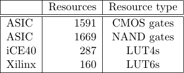 |
Even better, in spite of all the logic we dumped into this core, it still builds
into a rather small footprint, as shown in Fig. 36 to the right. In this
figure, the first line shows the number of CMOS gates, in total, that would be
used by this core with all options on, RDDELAY=0, and OPT_CLKDIV=7. The
second line is the same, but limited to measuring the number of
NAND gates the design would use,
were it to use nothing but
NAND gates,
flip flops
and NOT gates.
The third line, marked as iCE40, shows how many 4-input LUTs would be required
by a design with RDDELAY=0 and OPT_CLKDIV=0. This may be a rather
misleading statistic, though, since yosys
is known to pack logic into the reset circuitry present in the iCE40
flip flops.
The last line is a conservative estimate of the number of 6-input LUTs that
would be required in a Xilinx design–the actual
number is likely going to be much lower. Even in that case, it looks like
we’ve done pretty well! Indeed, this
controller
has a small logic foot print, just as we had desired from the beginning.
All that said, wow, that was a lot of ground to cover! We’ve now gone over
most of the
details in this flash
controller
from the ground up. We discussed the basic requirements of a good
flash controller, and
how to build one that ran at a high speed. Yes, this does run roughly twice
the speed of the Xilinx default
flash controller–if your board allows you to run the SCK pin in ODDR mode.
We also went though how to then modify that initial basic controller that we
started with to handle burst reads, getting into the
QSPI
XIP read mode in the first place, sending arbitrary commands to the
SPI,
and even how to handle I/O delays from using registered I/Os. Once we were
finished, I discussed all of the steps necessary to debug this new flash
controller.
No, I haven’t discussed the vendor specific I/O drivers. You should be able to find a decent discussion of them in the respective vendor literature. Instead, I’m trying to keep this blog somewhat vendor independent.
In practice, while I really like how easy it is to port this flash controller from one design to the next, the debugging bus that this depends upon is horrendously slow. Particularly slow are the steps necessary to determine if an erase step is required, or to determine that either the erase or programming steps were successful. Both of these are ideal tasks for a small program running within the FPGA, so if we continue this discussion that might be where we end up next.
Also, as more of a side note, I don’t normally write blog articles this long. This has taken several weeks to write, and is likely going to take you a long time to read. My apologies to you if this isn’t what you are looking for. I’ll try to keep future posts shorter. That said, my prayer for you is that this post will all be worth your while as well, so that you might either trust my own “Universal” flash controller now, or if not that you would at least have a good idea of where to start from when building your own.
One final note, there’s a reason why I’m calling this a “Universal” flash controller, controller, with the “Universal” in quotations. As currently built, this controller will be able to properly interact with all of the flash chips I’ve seen to date. However, I haven’t tested it on every chip in order to be able to prove that it truly is Universal. Moreover, I am aware of other classes of flash devices for which I already know this controller will not work. Still, I like the term “Universal”–even if I have to place it in quotation marks.
God, who at sundry times and in divers manners spake in time past unto the fathers by the prophets, Hath in these last days spoken unto us by his Son, whom he hath appointed heir of all things, by whom also he made the worlds (Heb 1:1)