
Getting Started with the Wishbone Scope
Ever found yourself stuck with an FPGA design that didn’t work and no idea why not? This seems to be a common problem within FPGA design. Perhaps the design works within a simulator. Perhaps you don’t know how to simulate the hardware component the design is working with. Either way, you will want to know how to somehow draw information out of the broken design to see where it fails.
We’ll show an example of how to do that here, using two primary components to make this happen. The first is any device or simulation imeplementing a generic DEVBUS interface into a wishbone bus implemneted within your FPGA. If you don’t have such an interface as part of your design, the HEXBUS interface should still suite your purposes nicely, although it will require a serial port to communicate on. The second necessary component is a wishbone scope, which you can access using the DEVBUS interface.
There are two parts required to adding a wishbone scope into your design, the Verilog integration and the software component. The first part is to connect the scope to your design: both by selecting wires from within your design that you wish to examine, as well as identifying trigger logic within your design to know when to capture those wires. (The block RAM used to capture a trace isn’t unlimited.) The second part is the logic necessary to read that capture off of the FPGA, and format it into a VCD file that you can use to view your data on a clock for clock basis using gtkwave.
We’ll walk through the two steps separately, and then show an example of using them to view a bus interaction.
Changes to your design
There are only four basic changes to your design that you’ll need to make in order to connect a wishbone scope into your FPGA design.
First, you’ll need to add the scope to your wishbone interconnect within your design. This involves six basic points of adjustment:
-
You’ll need to decode the scope’s address. I like to create an address select line (not to be confused with the byte SELect linse), indicating that the current address references the scope. Make sure that ADDR[0] is not a part of this computation, as the scope needs that line to determine which internal register is being accessed.
-
You’ll need to add the scope to the design, and wire the wishbone inputs to the scope. The STB line from the wishbone master needs to be gated (anded) with the address select logic result. The scope requires only one ADDR bit, so no others need to be connected. The wishbone outputs: ACK, STALL, and DATA will be declared and connected.
-
The ACK line needs to be logically OR’d with other ACK lines within your design. This logic should already exist, if you have a working wishbone interconnect, so follow along there and see what’s required.
-
As with the ACK, the DATA line needs to be integrated into the bus data return. In particular, the bus data return to the master should contain the scope’s data anytime time the scope’s ACK line is true.
-
Because the wishbone scope will never stall the bus, you can technically ignore the STALL line. For form and maintainability, though, you’ll probably want to use this line to create the wishbone master’s STALL return line. This is usually created by a large OR of every device’s address decode line AND’ed with their STALL line.
-
I often use a touch of logic to determine whether or not many ACK’s are begin returned at once, if more than one device is selected, or if no devices are selected. This logic will need to be adjusted as well.
If you are going to use the scope that already exists within the DBGBUS’s test infrastructure, all of this logic has already been taken care of for you. For more details, we also discussed how to do this in the article on building a simple wishbone interconnect.
The second step is deciding what you wish to trigger on. This is as simple a piece of logic as you wish. Within the DBGBUS’s implementation, you’ll find a line that looks like:
assign scope_trigger = (mem_sel)&&(wb_stb);This triggers the scope on any attempt to reference the block RAM peripheral within the testbus, although what you choose to trigger on is up to you. Want to trigger on any time the wishbone error is set as an example? The following logic would do that:
assign scope_trigger = (wb_err);We’ll stick to the former, though.
Third, you’ll want to select those wires that you want to capture and record. These wires can be anything you are interested in within your design. In our case, we’re going to capture some signals from within the wishbone bus’s interaction.
assign	debug_data = { wb_cyc, wb_stb, wb_we, wb_ack, wb_stall,
		wb_addr[5:0], 1'b1,
		wb_odata[9:0],
		wb_idata[9:0] };
The wishbone scope fixes this amount of debug data at 32-bits per clock, otherwise we might have grabbed more of this bus interaction. If you need more, you should be able to using multiple scopes at the same time to achieve a wider capture.
As a final step, you can limit the
scope so that it only captures data any
time a particular bit is true within your design. This capability is very
useful for digital signal processing applications, where the data of interest
may not exist on every clock. This is the i_ce input to the scope.
For this simple example, we’ll keep this set to ‘1’.
While we aren’t going to reconfigure the basic wishbone scope for this example, there are several configuration parameters that can be set. These parameters include:
-
The log of the size of the memory within the scope, LGMEM. By default, this is set to 10, so by default the scope will use 2^10 words of block RAM. Powers of two from anywhere between 2^2 and 2^31 are possible–with the natural consequence being that your actual FPGA hardware will limit how memory you can actually use.
-
Whether or not the scope is synchronous with your wishbone clock or not. This is the SYNCHRONOUS flag. It defaults to true (
1). If you ever need to collect data on one clock and read it on another, then set this to zero. That will trigger the inclusion of a lot of clock transfer logic within the design.For our design, we’ll leave this at the default as a synchronous scope, but that will also require the same
i_clkparameter being passed to the core twice. -
The default holdoff parameter sets the initial holdoff of the scope. This holdoff parameter may be changed at a later time by simply writing the new holdoff to the control register. Setting it within a parameter just sets the initial value of the holdoff register.
If the holdoff is set to zero, the trigger will be aligned with the last data sample in the scope’s memory. As the holdoff time is increased, the trigger location will move towards the beginning of the scope’s memory.
As another way to put it, once triggered, the FPGA waits for a number of clocks given by the holdoff value before stopping its collect. Hence, a holdoff of zero can be used to capture any logic leading up to an event, whereas a holdoff of the size of the buffer will capture any logic immediately following an event.
The default parameter value for the default holdoff places the trigger near the middle of the collect.
That’s it! That’s all you need to do to set up a wishbone scope within the FPGA part of your design.
The software controller
To use the Wishbone scope, you’ll also want to set up a software controller to handle the communication between the design, and to reformat the result into whatever you wish it to be. This is the purpose of the scope software controller. It is also specific to the logic you’ve chosen to capture, so this section will show you how to set it up.
When I initially used the Wishbone scope in my earlier projects, all the scope controller ever did was to check that the scope had indeed been triggered, and then dump every piece of data that had been collected to the terminal.
At one time, I wrote a new software controller every time I needed a scope within my design. If you wander through my designs, you can even find examples of these older scope controllers, such as this example that I used when debugging an SDRAM controller. These controller’s, though, all had the same logic:
Step one: Check if the scope is ready to be read, and exit if not.
v = m_fpga->readio(R_SCOPE);
if (0x60000000 != (v & 0x60000000)) {
	printf("Scope is not yet ready\n");
	...
	exit(0);
}
Step two: Calculate the size of the scope and allocate a buffer
lglen = (v>>20) & 0x01f;
scoplen = (1<<lgln);
buf = new DEVBUS::BUSW[scoplen];
Step three: Read the scope’s memory from the FPGA, transferring it from the FPGA to a buffer on your local computer.
m_fpga->readz(R_SCOPD, scoplen, buf);Step four: Decode the scope’s data
for(unsigned i=0; i<scoplen; i++) {
	// Do something to printf buf[i] to the screen
	...
}
After a while, though, I found myself cut/copy and pasting the same code from one controller to the next. Just the code above created a lot of boilerplate.
To help get reduce the amount of boilerplate code, the scope now has a controller scope class. Since building that scope control class, the scope’s capabilities have significantly increased. For example, the scope controller can now create a VCD file. It can now identify which sample produced the trigger (thanks to some bench testing, and so it can place the inferred trigger into the VCD file as well. So let’s instead discuss how to interact with this scope controller object.
The first step to using this controller. framework is to create your own subclass of the controller. to desccibe your particular wire choices within your RTL logic.
For the example we are working with, we’ll call this controller subclass a MEMSCOPE–since it’s going to look at interactions with the block RAM memory.
class	MEMSCOPE : public SCOPE {
public:
	MEMSCOPE(FPGA *fpga, unsigned addr) : SCOPE(fpga, addr) {};
	~MEMSCOPE(void) {}
	...
The scope object is created with a pointer to the FPGA object implementing the DEVBUS interface, together with the address of where this scope is within our wishbone bus.
Two virtual methods then need to be overloaded. The first method, called decode(), simply decodes the scope wires onto stdout. This is where the printf() interface I used to use ends up. The difference, though, is that the class takes care of reading from the scope, calculating the memory address, as well as marking where the trigger is. To make this work, be careful not to end any of the printf()’s within your decode function with a newline.
virtual	void	MEMSCOPE::decode(DEVBUS::BUSW val) const {
	int	cyc, stb, we, ack, stall, addr, odata, idata;

	cyc   = (val >> 31)&1;
	stb   = (val >> 30)&1;
	we    = (val >> 29)&1;
	ack   = (val >> 28)&1;
	stall = (val >> 27)&1;
	addr  = (val >> 21)&0x3f;
	odata = (val >> 10)&0x3ff;
	idata = (val      )&0x3ff;

	printf("%s", (cyc)?"CYC":"   ");
	printf(" %s", (stb)?"STB":"   ");
	printf(" %s", (we) ?"W" :"R");
	printf("[@....%02x]...%03x->...%03x", addr, odata, idata);
	printf(" %s", (ack)?"ACK":"   ");
	printf(" %s", (stall)?"(STALL)":"       ");
}
The second method that needs to be overloaded is the define_traces() method. This is where the connection is made between your design and the VCD file the scope object can generate. To make this possible, the scope object offers a register_trace() function. register_trace() takes three arguments. The first is the name of the wire or trace that’s being defined. The second argument specifies how many bits the trace has of the 32 the scope has captured. The third and final argument specifies which bit position this value starts at. Hence, we can define all of our traces with a simple:
virtual	void	MEMSCOPE::define_traces(void) {
	register_trace("wb_cyc",    1, 31);
	register_trace("wb_stb",    1, 30);
	register_trace("wb_we",     1, 29);
	register_trace("wb_ack",    1, 28);
	register_trace("wb_stall",  1, 27);
	register_trace("wb_addr",   6, 21);
	register_trace("wb_odata", 10, 10);
	register_trace("wb_idata", 10,  0);
}
All that remains is to create and run this scope controller.
Creating it is simple, after connecting to your FPGA and creating an object supporting the DEVBUS interface, you can just create the new scope from a pointer to the DEVBUS and the FPGA address of the scope:
MEMSCOPE *scope = new MEMSCOPE(m_fpga, R_SCOPE);You can check whether or not the scope is ready to be read with a simple
if (!scope->ready()) {
	printf("Scope is not yet ready:\n");
	...
}
Otherwise we’ll simply print our results, and write out a VCD file:
else {
	scope->print();

	scope->writevcd("scopd.vcd");
}
That’s it! That’s all the software required to use the Wishbone scope and to capture and output a VCD file containing the scope information.
Trying it out
Let’s use this with the debugging bus interface example design, and show how we can pull the data we need out of the design.
You’ll first need to build the example design. To do this, you’ll need to have g++, Verilator, git, and GTKWave installed.
git clone https://github.com/ZipCPU/dbgbus
cd dbgbus
make
We’ll demonstrate grabbing the scope’s output while running the Verilator, simulation, although you could use this with your FPGA just as well. Indeed, if your FPGA is connected to the TCP/IP port that our Verilator, simulation is using, then you can interact with your FPGA with no changes. The first step will be to start the simulation in one window:
cd bench/cpp
./testbus_tb
Were you trying to do this on an FPGA, you’d instead use the netuart program to bridge a serial port on your FPGA to the TCP/IP port that our DEVBUS software interface will interact with.
Either way, your next step will be to move to another window and interact with your FPGA. If you are using the DBGBUS demo, you’ll need to either read or write from the memory to trigger the scope:
cd sw/
./wbregs mem 0xdeadbeef
Now that the scope has finished its collection (even in simulation it’s pretty quick from trigger to stop), let’s use our scope controller to grab the result:
./memscopeThis will take a couple of moments to read the data from the simulation. (It’s a lot faster when using real hardware.) On my computer it can take close to a full minute, but that might be very CPU dependent.
The result, though, will be a file scopd.vcd. To examine this, just type
gtkwave scopd.vcdWith a little work with gtkwave, here’s what our results look like:
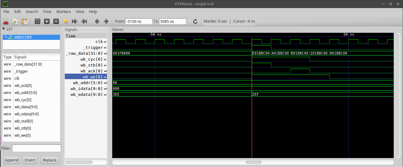 |
That’s it!
Did you see how easy that was? The only hard part was building the means to communicate between the FPGA and your host PC. After that, all that you really needed to do was to add the wishbone scope component to the wishbone bus within your design, and then define the traces you wanted to follow in your subclass of the software scope controller.
Stick around, though. Gisselquist Technology is working on a simpler way to connect your wishbone device components together using autofpga.
And the things that thou hast heard of me among many witnesses, the same commit thou to faithful men, who shall be able to teach others also. (2Tim 2:2)