
Building a basic AXI Master
 |
Over the course of the last year, I spent a lot of time on this blog discussing how to build AXI slave components. We discussed first how to verify an AXI-lite slave, and then how to build an AXI-lite slave that is neither broken nor crippled like Xilinx’s example IP packager design was. We then spent some time discussing the most common AXI mistake I’ve come across, AXI addressing and skid buffers. We could then examine Xilinx’s AXI slave, discover the bugs within it, and write our own slave with twice the throughput.
That’s all well and good for AXI slaves, but what about AXI masters? To date, we haven’t discussed the logic behind creating an AXI master on the blog at all. So, today, I thought I’d spend some time discussing how to build an AXI master that you could then use to interact with an AXI design.
Specifically, let’s discuss how to bridge from a Wishbone (WB) slave to an AXI master interface.
Classes of AXI Masters
 |
For the purpose of discussion, I’m going to divide AXI all master designs into one of four general categories or classes: single beat, single beat pipelined, bursting, and multichannel bursting. I’ve shown each of these four classes on the left in Fig. 2, together with their defining characteristics. In general, they are ordered from the least complexity to the most. Let’s take a brief moment, though, to look a bit deeper at the defining characteristics of masters written in each of these classes, and see how that affects both design and performance.
Single beat masters
A single beat master is an AXI master that issues requests, one at a time, and then waits for the response from that request before issuing a second request. These masters are perhaps the easiest masters to build, since you don’t need to keep track of how many transactions are outstanding at all.
 |
A good example of such a master is my recent AXI-lite master for the “hexbus”
debugging
bus.
This master uses the RREADY and BREADY signals as states in a state
machine to know whether or not it is in the middle of a read or write cycle.
Once the last acknowledgment is returned, the
core
returns to idle, lowers RREADY and BREADY, and is then ready to accept a
new burst request. Indeed, the trace shown in Fig. 3 above was drawn from this
core.
The key to this being a single beat master is that both AWLEN and ARLEN
are held at zero. This drastically simplifies the logic of the master:
1) you can hold WLAST high and ignore RLAST, and 2) you don’t need to worry
about the maximum burst length, whether or not your burst addresses are
incrementing or not, or whether or not the burst will cross a 4kB boundary.
Indeed, this is the easiest type of AXI master to write. Even more, you should be able to verify it using the AXI-Lite properties we’ve already discussed on this blog. Indeed, the induction property is quite simple: there’s either one burst outstanding on one of the two channels, or no bursts are outstanding at all.
Single beat pipelined
 |
The problem with single beat masters is simply throughput: you aren’t going to get much throughput from a single beat master. If that’s not a problem for your application, such as if you just need to create a simple AXI control script to control some minor AXI core, single beat masters are awesome. Forget the advice you’ve gotten from your vendor tech support, shown for reference in Fig. 4, just build a single beat master. If you want performance, however, then you will need to issue multiple requests without waiting for their responses. This is the purpose of the single beat pipelined master.
A single beat pipelined master will potentially issue multiple single beat requests before ever getting the first response, as illustrated in Fig. 5 below.
 |
There are two big differences between single beat masters and single beat pipelined masters. The first difference is that you really need a state machine to handle issuing requests and a separate state machine to handle request responses. You may even need a third state machine to coordinate the two, as we’ll see in a moment. The second big difference between the two is that the single beat pipelined master must maintain a counter of outstanding transactions and possibly even an internal FIFO to keep track of what needs to be done when the response returns.
In general, the single beat pipelined master is still fairly easy to design.
One key to the single beat pipelined processor, though, is that the AWID and
ARID fields need to be held constant. This will make sure your responses
get returned in order.
The biggest problem you’ll need to look out for with any single beat pipelined master implementation is that the counter of outstanding transactions cannot be allowed to overflow. This is easily caught by formal methods and specifically by an inductive proof. With simulation, you might instead be tempted to to set the number of bits in the counter to an arbitrarily large number just to keep the counter from overflowing. Sadly, this just creates the deceptive appearance that something works even when it doesn’t. You really need the formal inductive proof here to know that your design will always work.
Bursting, single channel
Single beat pipelined masters are awesome. They are the simplest masters that should be able to achieve the full speed of the bus.
The key word in that sentence is should.
Unfortunately, many AXI components are
optimized around burst processing and perform dismally with single beat
bursts. Xilinx’s AXI block RAM
interface
provides a perfect example of such a crippled core.
This block RAM core
requires 3+N clocks per burst, where N is the length of the
burst (AxLEN+1). As we’ll see in a moment, if your master interface doesn’t
support bursting, you’ll suffer from a 25% maximum throughput when interacting
with one of these cores.
Ouch!
Consider for example the trace shown below in Fig. 6, showing how three AXI bursts of four beats each requires 21 clocks to go through Xilinx’s block RAM interface.
 |
While this slave is able to handle one clock per beat of information, it can’t handle two bursts in short succession without taking some time to reset its internal logic. In this case, the core requires three clocks to reset and get ready for the next burst. With a 16-beat burst, perhaps 85% throughput isn’t really all that bad.
While 85% throughput might not be “that bad”, consider the throughput shown in Fig. 7 below, where this same core needs to respond to five separate AXI bursts for one beat of information each.
 |
Go ahead and count those clock cycles. For every ARVALID & ARREADY, the
core
requires three clock cycles before it will accept a new transaction. That’s
then one transaction every four cycles, to yield a 25% throughput. Yeah, ouch.
Didn’t you purchase your
FPGA
because you wanted raw processing speed? If this 25% throughput is
unacceptable to you, and it should be, then you’ll either need to fix this
(very crippled) AXI slave
interface, or adjust your
master to issue burst requests.
Bursts take more work since there’s a lot of rules associated with issuing
bursts in a protocol compliant manner.
The most obvious change is simply that you’ll now need to keep track
of both the number of beats outstanding as well as the number bursts
outstanding. The master will also need to carefully make certain that WLAST
is properly set on the last beat of every write burst.
Those are the easy changes. The more challenging changes have to deal with burst addressing and length calculations.
-
Bursts to or from a fixed address can be no longer than 16 beats in length. This applies to wrapped addressing as well. If the address increments, however, bursts of 256 beats are allowed.
-
Bursts are not allowed to cross 4kB boundaries.
Making sure bursts don’t cross 4kB boundaries, together with making certain that they are limited at 256 (or 16) beats, together with making certain that you only issue burst requests for the bursts you need, can become a very complex process. Sure, you could take two (or more) clocks to run your calculations, but then you might no longer be achieving 100% throughput.
No, the key or trick to this calculation, shared with me by one of my twitter followers, is to pick a maximum burst length that isn’t longer than 4kB, and then to align the start of all subsequent bursts on a burst length boundary. This will spare you from checking against both the burst length and the 4kB boundary before issuing a burst request.
-
For performance reasons you’ll also want to do your business and then get off the bus. Therefore, I recommend not ever attempting a bus transfer until you can make that transfer at 100% throughput within a burst.
Remember, every time your core is using the bus, there’s resources that need to be allocated to tracking that connection within the interconnect. If your core isn’t using the bus, those resources can be dedicated for other purposes.
While I hope to blog about how to do this eventually, you can check out some of my examples in the meantime. I have three examples of bursting AXI masters that you are free to examine if you are interested in more information. These are my AXI S2MM, MM2S, and DMA (MM2MM) cores. Compare, for example, the throughput these cores can achieve, as measured by my new AXIDMACHECK design design, with that of the crippled throughput achieved by the block RAM controller shown above.
 |
This figure, Fig. 8 above, shows a memory to stream master using the bus followed by a stream to memory master using the same bus and both interacting with an AXI block RAM core.
Notice how each master issues multiple burst transfers in a row, all at 256
beats each. You might also wish to note that the xVALID and xREADY
channels are high for extended periods of time. (Okay, the WREADY channel
has an issue due to the fact that we didn’t align the AW* and W* channels
within the slave–something
that would be easily fixed by adding a skid
buffer to the write
channel.)
I’ll also readily admit that comparing the AXI block RAM controller above with these DMA controllers going through an interconnect on to an optimized slave isn’t really a fair apples to apples comparison. My own AXI block RAM slave isn’t nearly as crippled as Xilinx’s AXI block RAM controller is. No, it’s not fair since the trace shown in Fig. 8 above also includes both master and interconnect. Still, you should be able to get the idea: if you are using AXI bursts, you should still be able to achieve 100% throughput even when crossing burst boundaries. Indeed, I might argue that you shouldn’t accept anything less.
As with the single beat pipelined master, this class of cores maintains
constant values for AWID and ARID for simplicity.
Bursting, multiple channel
The fourth type of
AXI
master is the one that adjusts AWID and ARID. This
class really describes a master that has multiple transaction sources internal
to it. Each transaction source makes requests of a different stream of data,
and in return can demultiplex those different streams back out based upon the
returned BID and RID values.
They key difference between constant AXI ID’s and varying AXI ID’s is that AXI only guarantees that returned responses will be in order when those responses have the same ID. In other words, if you use multiple IDs, you’ll never know which ID of the many transactions IDs you may have outstanding will be the next one returned.
At one time I had a nice example of a bursting, multiple channel master. That master would issue multiple requests with incrementing ID’s associated with them. The ID’s were then held in a sort-of random access FIFO that allowed values within to be returned in a random order. The FIFO structure then reordered the responses so that they would be returned in order.
I’ve since torn this master apart and replaced it with an implementation of the simpler bursting master logic that we’ll discuss the implementation of below.
Why did I tear it up and replace it? There were a couple of reasons. First, it was very difficult to verify that it worked. Yes, it worked in practice for about two years or so, but I couldn’t really verify that it would always work. Second, the reorder buffer slowed it down by adding an additional clock or two of latency to the logic.
Today, I only have one example of such a master, my AXI crossbar core. Sadly, that’s not really a very useful master to use as an example of how to build a bursting multiple channel AXI master. Worse, from an example point of view, my crossbar implementation doesn’t exploit the ID’s to its advantage at all. In its current implementation, it just forwards the ID’s downstream. While this is a protocol compliant approach, the crossbar doesn’t benefit from the purpose of the ID’s when doing so. (Yes, I’m hoping to fix this, feel free to check back with me later on whether or not I’ve updated this, and if so what the cost was of doing so.)
Where multiple channel AXI masters really start to shine is if a single master needs to access multiple slaves. Imagine an interconnect, that doesn’t truly support IDs, such as my current AXI crossbar implementation. In such an interconnect, a master might issue two requests: one for slave 1, and then a second one for slave 2. The interconnect that doesn’t support ID’s must first route the request to slave 1 and then wait for the response from slave 1 before routing the second request to slave number 2, as shown in Fig. 9 below.
 |
If the first slave takes a long time, the second request will be stuck behind that first one until that reply comes back. In the example shown in Fig. 9 above, the first slave takes four clocks to return. This keeps the interconnect from routing the second packet to the second slave until this first response returns. The second packet, therefore, suffers from a delay of seven clock cycles, when a single clock cycle delay might have been possible.
On the other hand, if the interconnect, were to provide full ID support, it should route the first request to slave 1, and then route the second request to slave 2 even before slave 1 responds.
 |
Unfortunately, while this looks faster in our figure above, the complexity
of the operation coupled with the desire for high clock speeds makes it so
that this form of
interconnect,
isn’t necessarily faster at all. For example, the
interconnect,
must now make certain that it keeps track of outstanding requests of every
<master,ID> combination, rather than one counter per master. It needs to
know to what slave such <master,ID> pairs are assigned to, as well as the
number of outstanding transactions assigned to that slave. This counter
is required to prevent a request from the same <master,ID> from being sent
to a subsequent slave and returning before the first slave’s response
returns. This means it needs 2^{IDW}*(num masters) counters, which might
each need to be updated on every cycle.
To make matters worse, what happens if both slave one and slave two respond to the same master at the same time? One of those two requests will need to be stalled. This return arbitration is likely going to cost another clock, and another skid buffer.
That leads to two obvious results of all of this extra logic: First, all logic within an FPGA or an ASIC has a cost. You’ll pay for this extra cost. Second, just because it sounds better on paper doesn’t mean it truly is in practice.
There’s a third cost as well: Xilinx’s demonstration AXI slave, generated by their IP packager, will break if ever driven by a bursting multiple channel master. It will also break in a busy environment when driven by an interconnect, that needs to arbitrate return responses. If your company uses designs built from these example designs, you’ll need to update them before upgrading your interconnect just to keep your design from suddenly seizing.
This leads me to the following summary comparing single vs multichannel masters, shown in Fig. 11 below.
 |
Put simply, I haven’t yet found an example that makes the cost, both in logic and latency, worth the price in complexity.
Designing a single beat, pipelined AXI master
 |
For today’s design, let’s focus on an AXI master that can handle single beat requests in a pipelined fashion. This would be the kind of AXI master you might write if you didn’t know from one beat to the next if another request would be coming, or even if so if you didn’t know where the next request would be made to. Alternatively, maybe you do know the address of the next address, but it doesn’t fit into any of AXI’s predetermined next burst address choices. Perhaps your are examining an image down the rows rather than across the columns. Perhaps you are attempting to feed a convolutional neural network from voxels in a three dimensional space. If for whatever reason you find yourself unable to use bursts, this class of AXI master should work nicely for you.
The good news for all of these applications is that Xilinx’s SDRAM MIG controller controller can handle single beat random access requests for reads or writes (not both) with 100% throughput–depending of course upon your access pattern. This is based upon my own experience with it. The bad news is that their AXI block RAM controller cannot, as discussed above.
We’re going to go a bit beyond that minimum requirement today, however, and discuss a Wishbone (pipelined, not classic) to AXI bridge such as you might wish to use to access a MIG memory core from Wishbone. Due to the specifics of our Wishbone bus implementation, this is going to force some additional requirements on the bridge.
-
Wishbone only allows a single request, either read or write, at a time. AXI allows independent read and write channels. In order to make certain we maintain the correct ordering between read and write responses, this core will only ever accept read requests or write requests. Further, all requests will be flushed before switching between the two.
Yes, we could go faster by keeping track of which requests we issued and in what order, but we’ll try to keep things a bit simpler today.
-
My own Wishbone implementations allow a bus abort. By this, I mean that if a Wishbone master wants to abort all outstanding transactions, it can do this by just dropping the cycle line for one clock cycle. After that, all pending acknowledgments need to be suppressed.
Unfortunately, AXI offers no similar capability. This is the reason why so many individuals have struggled to reset AXI DMA cores: if your AXI slave is broken, the DMA might hang. However, you can’t reset the DMA while a transaction is outstanding–no matter what the DMA instructions might tell you. AXI requires one bus response for every bus request.
This will mean that we need to keep track of the number of outstanding AXI responses, in case the Wishbone master ever wish to abort an outstanding transaction, and so keep subsequent responses from producing Wishbone acknowledgments.
 |
-
I also insist that every Wishbone master must issue a bus abort following any bus error. While the Wishbone specification doesn’t necessarily require this, my own implementations do.
In many ways, this just makes sense. What should a CPU do on a bus error? In general, the “right” answer is to halt the program at the first bus error return. What should a DMA do on a bus error? It should halt the transfer as soon as possible on the first erroneous return.
-
There’s one more piece of logic in this bridge that isn’t necessarily required by a generic bridge, and we’ll gloss over it below: this bridge will also (optionally) cross from a smaller bus size to (possibly) a much larger bus size. The reason for this is quite simple: I use this core to drive the AXI interface of an MIG generated SDRAM controller, and the natural width provided by the SDRAM tends to be much larger.
Yes, I suppose I could use one of the AXI size adjustment bridges within Xilinx’s interconnect. I could, but it doesn’t really make sense to. The size adjustment is just a minimal amount of logic yet it requires a FIFO and a clock of latency in each direction. If I can merge those clocks together, I can then reduce the overall latency in my design.
Were it not for these changes, this AXI master design would be really simple:
- Set the WB stall signal so that we’ll stall if any request is waiting to be sent forwards. This is perhaps the most complex part, since there are many reasons why we might need to stall the upstream bus. Let’s walk through each of them.
	always @(*)
	begin
		o_wb_stall = 0;
First, we might stall if ever the AW channel is stalled.
		if (o_axi_awvalid && !i_axi_awready)
			o_wb_stall = 1'b1;
We might also need to stall for essentially the same reason if the write data channel is stalled.
		if (o_axi_wvalid && !i_axi_wready)
			o_wb_stall = 1'b1;
The same applies to the read address channel.
		if (o_axi_arvalid && !i_axi_arready)
			o_wb_stall = 1'b1;
If you are counting combinatorial logic bits, like you should be, then we are now at six bits. That’s not really so bad, it fits nicely in just one 6-LUT.
Only … we haven’t yet added our extra requirements. Specifically, if we are waiting on read (or write) returns and we now want to reverse the direction of the bus, then we need to stall until the system is flushed enough that we can reverse the bus direction.
		if ((i_wb_we != direction)&&(!empty))
			o_wb_stall = 1'b1;
Remember, we’ve chosen the approach that we’ll only ever go in one direction at a time, and we’ll flush the design before switching directions.
Finally, if we are in the process of flushing all bus returns following a bus abort, or if our counter is about ready to overflow, then we’ll need to stall the incoming bus as well.
		if (flushing || nearfull)
			o_wb_stall = 1'b1;
	end
Since that’s a lot of logic, we’ll be using a skid buffer below to make sure it gets registered before leaving our core.
- On any Wishbone.
write request, where
i_wb_stb && i_wb_we, setAWVALID,WVALIDAWADDR, andWDATA.
	always @(posedge i_clk)
	if (i_reset)
	begin
		// Always clear any handshaking signals on reset.
		//
		o_axi_awvalid <= 1'b0;
		o_axi_wvalid <= 1'b0;
	end else if (i_wb_we && i_wb_stb && !o_wb_stall)
	begin
		// On any new write request, set both AWVALID and AWREADY
		o_axi_awvalid <= 1'b1;
		o_axi_wvalid  <= 1'b1;
	end else begin
Once each of these gets accepted, we’ll clear it to prepare for the next transaction.
		if (i_axi_awready)
			o_axi_awvalid <= 1'b0;
		if (i_axi_wready)
			o_axi_wvalid <= 1'b0;
	end
Always be aware, when building a cascaded if structure like this, of what
would happen in an earlier if statement were true. In this case, o_wb_stall
will keep us from setting both AWVALID and WVALID if ever one of the
two is still stalled from a prior request. Otherwise, it would preempt the
clearing of one of the two, and so it allows us to send multiple requests
on consecutive clock cycles.
This was what we wanted.
Let me pause here for a moment to note that this is the structure your
logic will need–even if you are building a pipelined master for a different
purpose. Surprisingly, this write logic structure doesn’t change much from
one design to the next. 1) You always want to reset any *VALID
signals. 2) You’ll always want to set both AWVALID and WVALID together
on any new write request (even if the
spec doesn’t require that they be
synchronized). 3) Once the
the appropriate *READY line has been raised, you’ll want to clear each of
AWVALID and WVALID individually. 4) Don’t start a new request
until both would otherwise be clear on the next cycle.
Not all designs keep the write address and write data channels synchronized. I find that it’s easier to verify the designs if the two channels are synchronized, so we’ll force them to be synchronized here by not initiating any new transactions until both signals from the last transaction have been accepted. Further, as I’ve learned from my new DMA testbed project shown in Fig. 8 above, if you don’t keep the two write channels synchronized, then the entire write operation will be slowed down every time a slave needs to synchronize them.
Moving on to the write channel, the logic is similar but subtly different.
	always @(posedge i_clk)
	if (!o_axi_wvalid || i_axi_wready)
	begin
		o_axi_wdata <= i_wb_data;
		o_axi_wstrb <= i_wb_sel;
	end
While you might reset any data associated with a request as well, it’s not
necessary to do so. In an effort to keep our logic low, we’ll set both
WDATA and WSTRB above any time the channel isn’t stalled. This isn’t
necessarily the low power approach. If you wanted lower power, you
would want to minimize the number of transitions on your wires–particularly
on any bus wires. Adding a
little bit of logic here to make that happen isn’t all that hard,
	always @(posedge i_clk)
	if (i_wb_stb && i_wb_we && !o_wb_stall)
	begin
		o_axi_wdata <= i_wb_data;
		o_axi_wstrb <= i_wb_sel;
	end
but in this case it just makes timing more difficult. Remember, for example,
that o_wb_stall had a rather large computational burden on it already.
This is why I chose to gate these values on (!o_axi_wvalid || i_axi_wready)
instead.
Setting AWADDR is a touch more difficult, simply because
Wishbone is word
addressed whereas AXI is byte addressed.
Hence, we’ll need to take the
Wishbone
address and append some number of zeros to it.
	localparam	DW = 32; // Wishbone data width

	// ...

	wire	[$clog2(WB_DATA_WIDTH)-4:0]	axi_lsbs = 0;

	// ...

	always @(posedge i_clk)
	if (!o_axi_awvalid || i_axi_awready)
		o_axi_awaddr <= { m_addr, axi_lsbs };
Note that this also follows the same logical structure that WDATA followed
above: the address gets updated if ever the channel isn’t stalled. As before,
a lower power approach exists, but I’ve chosen to go with the lower logic
approach here.
- Read requests are similar. On any read request, where
i_wb_stb && !i_wb_we, setARVALIDandARADDR.
Setting ARADDR is identical to what we did before with AWADDR, but
ARVALID is just a touch different simply because we don’t have two channels
that need synchronization.
	always @(posedge i_clk)
	if (i_reset)
		// Clear on any reset
		o_axi_arvalid <= 1'b0;
	else if (i_wb_stb && !i_wb_we && !o_wb_stall)
		// Set on any request
		o_axi_arvalid <= 1'b1;
	else if (i_axi_arready)
		// Clear once the request is accepted
o_axi_arvalid <= 1'b0;- As long as the bus widths are the same, we can just return the read values.
	always @(*)
o_wb_data <= i_axi_rdata;- Wishbone
has no ability to stall any returns. This makes setting any
o_wb_ackoro_wb_errsignal easy.
Unlike AXI,
Wishbone has two return
signals, ack and err. AXI has a
valid signal together with a 2-bit status captured by the xRESP signal. Of
the four possible status returns, we only care if the top bit is high
indicating an error. Hence, we
can write:
	assign	o_wb_ack = !flushing && ((i_axi_bvalid && !i_axi_bresp[1])
				||(i_axi_rvalid && !i_axi_rresp[1]));

	assign	o_wb_err = !flushing && ((i_axi_bvalid && i_axi_bresp[1])
				||(i_axi_rvalid && i_axi_rresp[1]));
The big difference here from what might otherwise be a simple return is
this flushing signal. I use this signal as part of the core’s reset
logic. If we are ever
flushing the pipeline, then we want to ignore any and all acknowledgments
as we return back to an idle
state.
- Given that Wishbone has no ability to stall the return acknowledgment, we can also hold the respective backpressure signals high.
	assign	o_axi_bready = 1'b1;
	assign	o_axi_rready = 1'b1;
Indeed, I’d recommend you hold these signals high in any master you build. If you hold these constant, you might be able to get the optimizer to remove any return skid buffer that might be within the interconnect. That said, I haven’t consistently held these values high within my own designs. While my AXI S2MM and MM2S cores do hold these high, my AXI-lite debugging bus master captures state information within these two ready signals so adjusting the logic so as to hold these signals high would require some rework.
Well, at least that’s the basics.
There’s one ugly trick remaining, and that is counting the number of transaction returns we are expecting so that we can 1) flush the channel on any error or bus abort, and 2) know that the channel is clear in order to change direction.
The reason why this is ugly is that any time you place a counter within your design, a counter that should never overflow, then you also need to place a check within your design to make certain that the counter truly never overflows. Don’t forget this check!
Our basic counter will count up any time o_wb_stb && !o_wb_stall, and
down any time BVALID || RVALID.
	always @(posedge i_clk)
	if (i_reset)
		npending <= 0;
	else case({ (o_wb_stb && !o_wb_stall), (i_axi_bvalid || i_axi_rvalid)})
	2'b01: npending <= npending + 1;
	2'b10: npending <= npending - 1;
	endcase

	assign	empty = (npending == 0);
	assign	full == (npending == (1<<LGFIFO));
	assign	nearfull == (npending == (1<<LGFIFO))-1;
Or at least that’s the idea. In my implementation
below,
I’m going to register empty, full, and nearfull so that I don’t
burden the logic on any subsequent
clocks
with those calculations.
Once we know when there are no requests outstanding, we can then keep track of direction. Specifically, we can change direction any time there’s nothing pending.
	always @(posedge i_clk)
	if (empty)
		direction <= i_wb_we;
That leaves us with only one more piece of logic: when do we need to flush the bus pipeline of any pending requests?
	initial	flushing = 0;
	always @(posedge i_clk)
	if (i_reset)
		flushing <= 0;
On any read or write error, we’ll want to start flushing the pipeline–since we are assuming that the Wishbone master will immediately abort any ongoing bus transactions following an error return.
	else if ((i_axi_rvalid && i_axi_rresp[1])
		||(i_axi_bvalid && i_axi_bresp[1])
Similarly, if the master ever drops the cycle line while a request is pending then we’ll also want to flush any ongoing operations.
		||(!i_wb_cyc && !empty))
		flushing <= 1'b1;
Once the pipeline has been flushed and there are no more outstanding transactions, then we can return to servicing incoming requests.
	else if (empty)
		flushing <= 1'b0;
Or, at least that’s a brief overview of how
this core
would work if it were really that simple. In general, your own core may
easily follow the same structure, since this isn’t all that different from any
AXI master in general. At least it’s
not that different from any other AXI
master that 1) holds the AxID fields constant, and 2) holds AxLEN==0.
Notice also that setting the the Ax* register fields was fairly simple.
Handling returns wasn’t that hard either. The big trick to this
core
is the counter that counts the number of ongoing transactions.
Imagine that: after years of studying FPGA designs you find that the tricky part of the design turns out to be a counter, the very same thing you studied back on day one when you started learning digital logic.
AXI Master Logic
It’s now time to walk through the logic of
the core
itself. As we do this walk through, you’ll see a couple big differences
from the conceptual logic we quickly sketched above. The first big
difference is that we use a
skid buffer
on the input to reduce the timing burden on the actual o_wb_stall signal.
The second big difference is that this
core can
handle an upsizing data width conversion. This would be really easy, save for
selecting the correct subword from the returned data word. The last big
difference is that several of the transaction counter flags are registered.
Perhaps these differences really aren’t all that big. Either way, let’s start our walk through in detail.
The bus
interconnect
generator, AutoFPGA
in this case, knows the size of the
bus widths this
core connects
to. The parameters C_AXI_DATA_WIDTH and DW capture the width of the
AXI
bus and the
Wishbone
bus respectively. In a
similar manner, C_AXI_ADDR_WIDTH and AW capture the address widths of the
two busses, AXI and
WB respectively,
as well.
module wbm2axisp #(
	parameter C_AXI_DATA_WIDTH	= 128,// Width of the AXI R&W data
	parameter C_AXI_ADDR_WIDTH	=  28,	// AXI Address width (log wordsize)
	parameter C_AXI_ID_WIDTH	=   1,
	parameter DW			=  32,	// Wishbone data width
	parameter AW			=  26,	// Wishbone address width (log wordsize)
	parameter [C_AXI_ID_WIDTH-1:0] AXI_WRITE_ID = 1'b0,
	parameter [C_AXI_ID_WIDTH-1:0] AXI_READ_ID  = 1'b1,
	parameter LGFIFO		=   6
	) (
	input	wire			i_clk,	// System clock
	input	wire			i_reset,// Reset signal,drives AXI rst
The two IDs, AXI_WRITE_ID and AXI_READ_ID, will contain our constant
AXI ID values–assuming the
interconnect even uses them.
The LGFIFO parameter captures the size of the FIFO above. You can think of
this as the log of the number of transactions you might have outstanding, the
bit width of our transaction counter if you will. It’s more than that though.
When doing a data conversion, even going up, you need to keep track of the
low order address bits in order to be able to select the correct data word
on return. This requires a per-beat FIFO, and LGFIFO also keeps track of
the log of the number of elements in our FIFO. At LGFIFO=6, we can keep
track of 64 outstanding transactions. That’s enough latency that we shouldn’t
need to worry about being impacted by the (horrendous) latency of the MIG
SDRAM controller.
We can simplify some of these parameters as well here. In particular, the
conversion from a word based address to a byte based address on a
bus that might not be the same
size is going to take a bit of help. These localparams will help simplify
that conversion.
	localparam	LG_AXI_DW	= $clog2(C_AXI_DATA_WIDTH);
	localparam	LG_WB_DW	= $clog2(DW);
	localparam	FIFOLN = (1<<LGFIFO);
	localparam	SUBW = LG_AXI_DW-LG_WB_DW;
It’s important to note that the address widths of the two busses are coupled
in a way that’s not really captured by the parameters above. In particular,
the AXI address width must be equal to
the Wishbone address
width plus the number of subword address bits. (Note that the
AXI address width doesn’t change as the
bus changes data widths,
unlike the Wishbone
address width.) Here, we can use the Verilog $stop function to make certain
that the design won’t even build if the parameters aren’t set up properly.
	initial begin
		if (C_AXI_DATA_WIDTH < DW)
			$stop;
		if (C_AXI_ADDR_WIDTH != AW + $clog2(DW)-3)
			$stop;
		if (	  (C_AXI_DATA_WIDTH / DW !=32)
			&&(C_AXI_DATA_WIDTH / DW !=16)
			&&(C_AXI_DATA_WIDTH / DW != 8)
			&&(C_AXI_DATA_WIDTH / DW != 4)
			&&(C_AXI_DATA_WIDTH / DW != 2)
			&&(C_AXI_DATA_WIDTH      != DW))
			$stop;
	end
Most of the bus wires don’t ever need to be changed. The more values we fix like this, the simpler our logic will be below.
	localparam	DWSIZE = $clog2(DW)-3;
	assign o_axi_awid    = AXI_WRITE_ID;
	assign o_axi_awlen   = 8'h0;	// Burst length is one
	assign o_axi_awsize  = DWSIZE[2:0];
	assign o_axi_wlast   = 1;
	assign o_axi_awburst = 2'b01;	// Incrementing address (ignored)
	assign o_axi_awlock  = 1'b0;	// Normal signaling
	assign o_axi_arlock  = 1'b0;	// Normal signaling
	assign o_axi_awcache = 4'h2;	// Normal: no cache, no buffer
	assign o_axi_awprot  = 3'b010;	// Unpriviledged, unsecure, data access
	assign o_axi_awqos   = 4'h0;	// Lowest quality of service (unused)
	//
	assign o_axi_arid    = AXI_READ_ID;
	assign o_axi_arlen   = 8'h0;	// Burst length is one
	assign o_axi_arsize  = DWSIZE[2:0];
	assign o_axi_arburst = 2'b01;	// Incrementing address (ignored)
	assign o_axi_arcache = 4'h2;	// Normal: no cache, no buffer
	assign o_axi_arprot  = 3'b010;	// Unpriviledged, unsecure, data access
	assign o_axi_arqos   = 4'h0;	// Lowest quality of service (unused)
In particular, you should note that we’ve held the AxID values constant,
and that AxLEN == 0 for every burst. These are the two defining
characteristics of this particular class of AXI
master.
They also allow me to simplify the WLAST calculation, and simply hold that
signal high above. Similarly, the AxSIZE parameter is set based upon the
size of the Wishbone
bus,
$clog2(DW)-3. You might wish to note that by referencing a bit-range
within a constant localparam, I’ve been able to get past the bit-width warning
Verilator
might otherwise produce.
Most of the rest of the signals above will be ignored by the large majority
of AXI components out there. In general
they can be set to 0, although I’ve tried to be a bit fancier here by setting
AxPROT to 3'b010 and AxCACHE to 4'h2. I haven’t really had any good
feedback, either from the AXI
specification or any cores that
depend upon these values, to know if they’ve been well chosen or not.
I mentioned above that I’d need to know the number of bits that needed to be
set to convert a WB
address to an AXI address. In order to
avoid setting these bits to {($clog2(DW)-3){1'b0}} every time, I’ve created
a simple helper value in axi_lsbs.
	wire	[$clog2(DW)-4:0]	axi_lsbs;
	assign	axi_lsbs = 0;
I don’t normally discuss register declarations here, but I did want to make one point regarding the following declarations.
	reg			direction, full, empty, flushing, nearfull;
	reg	[LGFIFO:0]	npending;
	//
	wire			skid_ready, m_valid, m_we;
	reg			m_ready;
	wire	[AW-1:0]	m_addr;
	wire	[DW-1:0]	m_data;
	wire	[DW/8-1:0]	m_sel;
After finding one major vendor tool that couldn’t properly handle a reference to a register that was defined later in a design, I’ve been slowly converting all of my designs so that the register or wire declarations are all done at the top of every module and before any logic that might reference them. Yes, this simple “language feature” that was treated differently by diffferent tools led to simulation/synthesis mismatch. By declaring my registers up top, I should be able to help avoid that again in the future.
The second thing to comment on are the m_* signals. In order to simplify the
WB
bus, I added a
skid buffer.
As we’ll see further down, these m_* signals capture the outputs of that
skid buffer,
so they should (roughly) mirror the i_wb_* signals. (The names aren’t
perfect matches, though, since I’m using m_value to mirror i_wb_stb.)
As discussed above, if ever nothing is pending we can change the direction the design is going in.
	initial	direction = 0;
	always @(posedge i_clk)
	if (empty)
		direction <= m_we;
Here’s the first big change from above. Remember the count of outstanding transactions? Here’s that count again, only this time we’re going to keep track of and register all of the other associated signals along the way.
	initial	npending = 0;
	initial	empty    = 1;
	initial	full     = 0;
	initial	nearfull = 0;
	always @(posedge i_clk)
	if (i_reset)
	begin
		npending <= 0;
		empty    <= 1;
		full     <= 0;
		nearfull <= 0;
	end else case ({m_valid && m_ready, i_axi_bvalid||i_axi_rvalid})
	2'b10: begin
		npending <= npending + 1;
		empty <= 0;
		nearfull <= &(npending[LGFIFO-1:1]);
		full <= &(npending[LGFIFO-1:0]);
		end
	2'b01: begin
		nearfull <= full;
		npending <= npending - 1;
		empty <= (npending == 1);
		full <= 0;
		end
	default: begin end
	endcase
I should note that I’ve now debugged several student designs that have
gotten this simple logic wrong. It’s not if (m_valid && m_ready) then
increment the counter, else if (bvalid||bready) decrement it. This seems
to be a common mistake. Don’t forget the likelihood that both might be true
at the same time! Verilog design is not software design, everything runs in
parallel.
Don’t let the the m_valid signal look new at all. It’s simply a replacement
for the i_wb_stb signal but on the other side of the
skid buffer, since I
used the AXI handshaking terminology
when building my skid
buffer.
For that reasons, the m_ready signal is a !stall indicator at the same
interface.
The flushing logic matches what we discussed above. We start flushing the
design on any bus
error
or bus abort condition, and
then keep flushing until there are no more outstanding transactions. We’ll
use the formal tools to make certain we have this and our counter right
along the way.
	initial	flushing = 0;
	always @(posedge i_clk)
	if (i_reset)
		flushing <= 0;
	else if ((i_axi_rvalid && i_axi_rresp[1])
		||(i_axi_bvalid && i_axi_bresp[1])
		||(!i_wb_cyc && !empty))
		flushing <= 1'b1;
	else if (empty)
		flushing <= 1'b0;
That brings us to the skid buffer. We’ll send all of the incoming bus signals into the skid buffer. This allows us to present this design component to the interconnect using a registered stall signal, albeit while burdening the logic of the other incoming signals.
	skidbuffer #(.DW(1+AW+DW+(DW/8)),
		.OPT_OUTREG(1'b0))
	skid (i_clk, i_reset || !i_wb_cyc,
		i_wb_stb, skid_ready,
			{ i_wb_we, i_wb_addr, i_wb_data, i_wb_sel },
		m_valid, m_ready,
			{ m_we, m_addr, m_data, m_sel });

	always @(*)
		o_wb_stall = !skid_ready;
Let me pause here, though, to point out the !i_wb_cyc term in the
skid buffer’s
reset input. This is part of flushing the design in case of a
bus
abort–anything that hasn’t gone to the
AXI side of the design needs to be wiped
clean if ever !i_wb_cyc. (Yes, it took a couple times through with the
formal tools to get this right.)
Remember the o_wb_stall logic we worked through above? This is now the
m_ready logic below. It captures whether or not we are ready to accept
a signal from the skid
buffer or not.
	always @(*)
	begin
		m_ready = 1;

		if (flushing || nearfull || ((m_we != direction)&&(!empty)))
			m_ready = 1'b0;
		if (o_axi_awvalid && !i_axi_awready)
			m_ready = 1'b0;
		if (o_axi_wvalid && !i_axi_wready)
			m_ready = 1'b0;
		if (o_axi_arvalid && !i_axi_arready)
			m_ready = 1'b0;
	end
As you may rememeber, this ready signal was a key part of the simplified
AXI-lite design. It
fulfills the same basic function here, even though we’ve combined both
read and write channels when building it. The goal is simply that we know
we are accepting a
Wishbone signal into the
AXI
side of the interface anytime m_valid && m_ready are true together.
The AWVALID and WVALID logic below should match our logic above signal
for signal, save for the difference of using the outputs from the
skid buffer.
	initial	o_axi_awvalid = 0;
	initial	o_axi_wvalid = 0;
	always @(posedge i_clk)
	if (i_reset)
	begin
		o_axi_awvalid <= 0;
		o_axi_wvalid  <= 0;
	end else if (m_valid && m_we && m_ready)
	begin
		o_axi_awvalid <= 1;
		o_axi_wvalid  <= 1;
	end else begin
		if (i_axi_awready)
			o_axi_awvalid <= 0;
		if (i_axi_wready)
			o_axi_wvalid <= 0;
	end
The WDATA logic is slightly different as well. In this case, we assume
we are upsizing. We also know that
bus
sizes are only ever powers of two.
This allows us to just repeat our data register across o_axi_wdata.
The alternative, shifting m_data by an amount given in the low order bits
of m_addr, would be annoying to do and get right. Duplicating everything
is just the simple way to handle it.
	always @(posedge i_clk)
	if (!o_axi_wvalid || i_axi_wready)
		o_axi_wdata   <= {(C_AXI_DATA_WIDTH/DW){m_data}};
Here’s the ARVALID logic. Again, it’s much like you might expect.
	initial	o_axi_arvalid = 0;
	always @(posedge i_clk)
	if (i_reset)
		o_axi_arvalid <= 0;
	else if (m_valid && !m_we && m_ready)
		o_axi_arvalid <= 1;
	else if (i_axi_arready)
	begin
		o_axi_arvalid <= 0;
	end
The big thing to note about this ARVALID logic is that 1) it represents
a separate state machine from the RVALID logic below, and 2) we allow
multiple transactions to be outstanding.
We can also update the address registers any time the respective address channels aren’t stalled.
	always @(posedge i_clk)
	if (!o_axi_awvalid || i_axi_awready)
		o_axi_awaddr  <= { m_addr, axi_lsbs };

	always @(posedge i_clk)
	if (!o_axi_arvalid || i_axi_arready)
		o_axi_araddr  <= { m_addr, axi_lsbs };
Notice the !VALID || READY check. This one’s easy to mess up. In one
Xilinx ethernet design,
the designer only checked for READY, not !VALID || READY. The
design
would then fail in the presence of a multiple master-ID capable
interconnect
that had to arbitrate return responses. Further, it’s worth reflecting on the
fact that !VALID || READY is the negation of VALID && !READY,
AXI stall condition.
Hence, any time the respective address channels are not stalled,
then we want to adjust the addresses.
When it comes to setting WSTRB, I chose a rather verbose approach. If
the two data widths are the same, m_sel can just be copied to WSTRB.
If not, you need to be careful which WSTRB bits get set–since these
indicate which bytes will actually be written as part of the
AXI transaction.
Here’s the generate statement for two of the combinations.
	generate if (DW == C_AXI_DATA_WIDTH)
	begin

		always @(posedge i_clk)
		if (!o_axi_wvalid || i_axi_wready)
			o_axi_wstrb   <= m_sel;

	end else if (DW*2 == C_AXI_DATA_WIDTH)
	begin

		always @(posedge i_clk)
		if (!o_axi_wvalid || i_axi_wready)
		begin
			if (m_addr[0])
				o_axi_wstrb   <= { m_sel, {(DW/8){1'b0}} };
			else
				o_axi_wstrb   <= { {(DW/8){1'b0}}, m_sel };
		end

	end else if // ...
	// ...
	end endgenerate
As I mentiond above, if there was no data width conversion, then setting
o_wb_ack, o_wb_err, and o_wb_data were fairly straightforward.
	generate if (DW == C_AXI_DATA_WIDTH)
	begin : NO_READ_DATA_SELECT_NECESSARY

		always @(*)
			o_wb_data = i_axi_rdata;

		always @(*)
			o_wb_ack = !flushing&&((i_axi_rvalid && !i_axi_rresp[1])
				||(i_axi_bvalid && !i_axi_bresp[1]));

		always @(*)
			o_wb_err = !flushing&&((i_axi_rvalid && i_axi_rresp[1])
				||(i_axi_bvalid && i_axi_bresp[1]));
Where things get tricky are when we need to do a data width conversion.
Sending the right data down the write channel wasn’t that hard, but the
read channel is a touch harder. In particular, we’ll need a small FIFO
to keep track of the low order bits of the address–at least enough of a
FIFO to select the right subword from the returned RDATA value later.
	end else begin : READ_FIFO_DATA_SELECT

		reg	[SUBW-1:0]	addr_fifo	[0:(1<<LGFIFO)-1];
		reg	[SUBW-1:0]	fifo_value;
		reg	[LGFIFO:0]	wr_addr, rd_addr;
		wire	[C_AXI_DATA_WIDTH-1:0]	return_data;
Because of this difficulty, we’ll need to take an extra clock to select the data we want during the return. That means that the acknowledgment and bus error lines will need to be registered in order to keep things aligned.
		initial	o_wb_ack = 0;
		always @(posedge i_clk)
		if (i_reset || !i_wb_cyc || flushing)
			o_wb_ack <= 0;
		else
			o_wb_ack <= ((i_axi_rvalid && !i_axi_rresp[1])
				||(i_axi_bvalid && !i_axi_bresp[1]));

		initial	o_wb_err = 0;
		always @(posedge i_clk)
		if (i_reset || !i_wb_cyc || flushing)
			o_wb_err <= 0;
		else
			o_wb_err <= ((i_axi_rvalid && i_axi_rresp[1])
				||(i_axi_bvalid && i_axi_bresp[1]));
As you’ll see above, it’s not just a simple matter of registering these signals. They now need to be subject to the reset signal and the bus abort signal, in addition to the signals they were sensitive to before.
I suppose technically I might’ve only chosen to register the read return and not the write returns as well, since I’m preventing the AXI side from ever having both reads and writes outstanding. On second thought, though, the logic above is complex enough that I’m torn between whether or not to always register these return signals before leaving this core or not.
Now we need some FIFO logic. The good part of this is that our npending,
empty, and full signals above properly mirror the number of elements in
this FIFO. That will at least clear up some of the challenge of getting
the control signals right.
We’ll still need to adjust the address of the FIFO on any write.
		initial	wr_addr = 0;
		always @(posedge i_clk)
		if (i_reset)
			wr_addr <= 0;
		else if (m_valid && m_ready)
			wr_addr <= wr_addr + 1;
And we’ll still need to write the value we need into the FIFO. Here, we’re just grabbing the low order bits of the Wishbone address. These are the bits which we’ll need later to select which subword of the return data word is the one we need.
		always @(posedge i_clk)
		if (m_valid && m_ready)
			addr_fifo[wr_addr[LGFIFO-1:0]] <= m_addr[SUBW-1:0];
As with the write address above, on a read we’ll adjust the read address.
		initial	rd_addr = 0;
		always @(posedge i_clk)
		if (i_reset)
			rd_addr <= 0;
		else if (i_axi_bvalid || i_axi_rvalid)
			rd_addr <= rd_addr + 1;
Do note that neither of these FIFO addresses are subject to either bus errors or bus aborts. They live on the AXI side of the bridge, and so they don’t get reset whenever we need to flush the pipeline.
Since the FIFO is fairly short and the number of bits in each word are fairly small, we can use distributed RAM here. That means we can both read from the FIFO and use the value we’ve read from it on the same clock cycle.
		always @(*)
			fifo_value = addr_fifo[rd_addr[LGFIFO-1:0]];
The last step of this processing is to select the bus word we are interested in. If the sub-bits of our address were zero, those would be the low order subword. Remember, AXI stores the low address bytes in the least significant positions of their data word. That makes this shift easy to do.
		assign	return_data = i_axi_rdata >> (fifo_value * DW);
		always @(posedge i_clk)
			o_wb_data <= return_data[DW-1:0];

	end endgenerate
This isn’t really the end of the story. AXI is naturally a little endian bus. Yes, I know the spec says that it’s neither big nor little endian, but if you look at how words are laid out on the bus, words naturally end up in a little endian, setting. Wishbone on the other hand is also neither big nor little endian, but it doesn’t specifically state which bytes within a word are more or least significant.
If you ask me, the entire little endian format is messed up since I can’t see a number in it’s natural order from a hex dump: most significant byte first. As a result, I’ve built the ZipCPU so that it would be big endian from the beginning. Sadly, this also leaves me swimming upstream as I fight between my own view of the world and what seems to be the dominant view of the topic.
My point is simply this, I may need to come back through here later and swap the byte order of these various words if I really want to interact with AXI bus components. Thankfully, I haven’t needed to yet. Instead, I’ve been able to get by with what I call “word-endian” where as long as words are properly placed on the bus (MSB=MSB) then everything is good. Unfortunately, I’m fighting against the Borg here, and it’s not clear how much longer I’ll last before being assimilated.
The last step in this core is to make certain we hold the various ready signals high. As discussed above, this might permit the optimizer to reduce the amount of logic required surrounding this core–but there are no guarantees.
	assign	o_axi_rready = 1'b1;
	assign	o_axi_bready = 1'b1;
We’ll skip the formal methods check of this core today.
`ifdef	FORMAL
	//
	// ... Formal properties ...
`endif
endmodule
It’s not nearly all that hard to do, so I may come back and present it later. The big thing is that it depends upon my formal AXI property set–something that I’ve been known to offer to patron’s of the blog.
Performance
At this point you might be wondering, how did we do? So let’s look at a couple of traces to illustrate the kind of performance that’s possible–but that you aren’t likely to see in real life.
 |
Fig. 14 on the left shows the write performance going through the
core. I’ve
trimmed the figure down so you don’t see any of the constant signals associated
with this transaction. In particular, this trace and the ones following will
have AWREADY, WREADY, and ARREADY all held high. Don’t expect this in
practice when working either with an
interconnect
or any of Xilinx’s cores, but it’s nice when it does happen.
As you consider Fig. 14, pay close attention to the fact that both
AWVALID and WVALID, as well as by inference above
AWREADY and WREADY, are all high for multiple clocks in a row. This
is the key characteristic of any single beat, pipelined master.
Indeed, this is how bus components should work.
Note also how the write address and data channels are each synchronized. While this isn’t required by the protocol, it’s really the ideal configuration for high speed.
Looking at latency, you’ll notice a two clock loss. First, there’s a clock
taken between the
Wishbone request and the
AXI request. This follows from the
AXI requirement that outputs should
not combinatorially depend upon inputs, even though that’s not strictly the
case here since these are
Wishbone inputs and not
AXI inputs. Second, there’s another
clock lost between AWVALID and BVALID. This time, the clock lost is
required by the AXI protocol. Were we
to adjust the width of the return, we would lose another clock in the return
path as well.
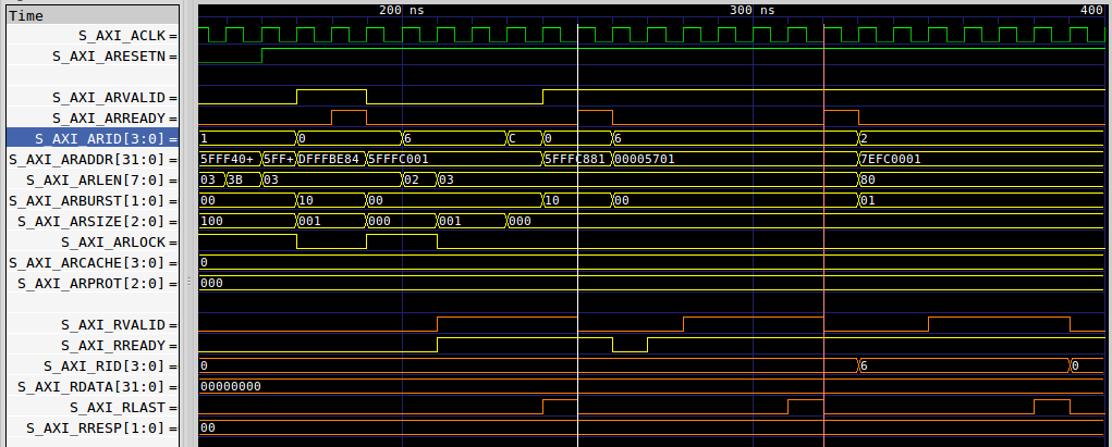
Let’s take a look at the read performance now, as shown in Fig. 15.
 |
Fig. 15 also shows a series of 3 transactions. As with Fig. 14 above, you may
assume that ARREADY is held high. Again, the key characteristic of
a single beat, pipelined master is that the master is issuing new read
requests before the first response has been received.
Of course, the amount of latency shown in Fig. 15 is also ridiculously and uncharacteristically low. The typical interconnect alone will add another four clocks of latency to any design. Still, this is decently representative of how the protocol should work on a good day.
Suppose we try again, but this time we attempt to stress our core a bit. In particular, let’s take a look at how fast we can issue four write requests followed by four read requests. Remember, we promised ourselves we’d flush the pipeline between these requests too. Worse, let’s insist that our buffer fill up with all four values along the way, so that we have had four values outstanding in each direction before returning.
This more complicated trace is shown in Fig. 16 below.
 |
Again, the key characteristic in this trace of this class of AXI master is that the master is capable of issuing multiple requests long before the first request comes back. In this case, the master allows four write burst beats to be outstanding. It then waits for the four write beats to be returned before issuing five more read beats. Even better, the latency shown in Fig. 16 is closer to what you are likely to see in reality, even if still a little short.
Conclusion
Some time ago we discussed measuring how fast a CPU could toggle an external I/O, and how this “blinky” test made tended to make a CPU look slow. There are three primary parts to the equation of how slow blinky appears to be. The first key is the bus master, and today we’ve seen how a high performance bus master might issue multiple commands to a bus slave without waiting for the first to return. This was a key reason why the ZipCPU was able to outperform both ARM and Microblaze in that test.
The other two items are just as critical. These are the interconnect and the slave. Just as a bus master can be written to only ever allow one burst to be outstanding at any given time, an interconnect can also be written this way as well. While such interconnects can easily be low-logic interconnects, they won’t permit high performance anywhere in your design. Sure, you can use them for sequencing or controlling high performance streams, but you won’t get high performance access to your SDRAM if you are going through an interconnect so conigured.
As for the last item, the bus slave, I don’t think it should come as a surprise to any one that a poor slave implementation, such as Xilinx’s AXI GPIO, isn’t going to provide good performance. Just for reference, here’s a trace showing that GPIO slave’s throughput.
 |
At one transaction every four clocks, it’s not very pretty.
Thankfully, if you’ve been reading this blog, you already know how to build a high speed AXI slave component that can knock the socks off of this GPIO slave.
Ho, every one that thirsteth, come ye to the waters, and he that hath no money; come ye, buy, and eat; yea, come, buy wine and milk without money and without price. (Is 55:1)