
RE: Building a simulation for my design? What does that mean?
Recently, a student wrote to me:
Hello. I am a student taking my first digital design course, and I stumbled upon your website. Specifically, this article.
What exactly is meant here when you talk about building a simulation for your design?
(I’ll keep the student’s name anonymous.)
 |
He’s specifically talking about an article where I discuss the student design process, as shown in Fig 1. on the right. If you haven’t read that article, I would commend it to you.
The article recommends having a valid/working simulation before ever moving to hardware. It also recommends using some form of debugging bus and/or internal logic analyzer for debugging designs that have moved to hardware. About the time the article was written, I was mentoring another college student who had been struggling through to build a design of his own. When he came across this article, he was kind enough to respond with his own experiences.
Sadly, this experience of frustration is common. It is so common, that I coined the phrase “FPGA Hell” to describe it, and then dedicated my blog to keeping students out of FPGA Hell. Much to my surprise, I’ve since spoken with many professionals who have been interested in these topics as well. Apparently, FPGA Hell in the business (i.e. ASIC) world can easily translate into millions of lost dollars–and often lost jobs as well.
But let me come back to the original question: what do I mean when I talk about building a simulation for a design? There are two types of simulations I have used in my designs.
-
Simulation in this context can reference a quick bench test of a module, that attempts to verify the module logic works.
I used to do this with my components a lot. I don’t do this as much any more. Why not? My own efforts just weren’t very effective at finding bugs.
That said, this remains my approach when debugging any DSP design.
-
It can also refer to an integrated test of the entire design and all of its pieces, together with co-simulations of all of the attached pieces of hardware. I do this before moving to actual hardware.
I continue this practice religiously, and every system level project I have has a full simulation capability. Depending on the project this simulation can either be found in the
bench/cppdirectory or a similarsim/verilateddirectory.
I’ve discussed simulation many times over on the blog, providing both examples of simulation, and discussing how I put simulations together. For example:
-
I use Verilator for all of my simulating needs. We’ve discussed how to build a verilator-based bench test already on this blog.
-
We’ve also discussed how to test a DSP filter design using Verilator as well.
-
The same applies to testing a CORDIC algorithm that can evaluate sine and cosine functions.
-
Did I mention discussing how to build a simulation for a logic PLL?
-
Verilator allows me to integrate C++ co-simulation code into my designs. (Verilator is not necessarily unique in this fashion, there are other approaches, however Verilator is most definitely my chosen approach.) Examples include:
– A serial port that you can connect to using TCP/IP, such as
telnet localhost <port #>. You can read about an example using this approach here.– A parallel port that takes the place of the serial port in my design for the ICO Board
– A VGA simulator: includes both source (i.e. a camera) and sink (i.e. a window on your screen) co-simulators.
– An A/D simulator for this microphone PMod.
– A flash simulator. This has been so useful, I’ve reused it just about all of my ZipCPU projects
– A SD-Card simulator (SPI mode only). When I finally get to implementing Linux on the ZipCPU, being able to simulate an SD card capability will be very important.
– An I2C simulator. This was a necessary part of my (still incomplete) HDMI design, since modern monitors are supposed to respond to a query and reply with the video formats they support. (The I2C part of the design works.)
– One of my designs even includes a GPS PPS signal simulator, for testing my GPS time-tracking algorithm(s).
-
I am a firm believer in building a simulation that you can interact with using a TCP/IP network port. This allows you to test/verify interacting with a design using your production software.
-
In one blog post I discuss how to run the ZipCPU in an environment using a simulated serial port.
This blog post also includes instructions for playing 4x4x4 Tic-Tac-Toe on the ZipCPU–running in simulation only. If you’ve never tried 4x4x4 Tic-Tac-Toe, I challenge you to try to beat the computer at the game. It’s not unbeatable, but the artificial intelligence used by that design is pretty good.
-
The VGA Simulation project contains code for two simulation components within it. (Both are Verilator based).
 |
- The main_tb simulator simulates an RTL design that reads from a frame buffer in memory and draws the contents of that frame buffer to the screen.
You can see an example of the window this draws on my screen in Fig 2 on the right.
The importance of having such a video simulation capability can not be understated. It is not that uncommon to have a bug in the graphics produced by a video-enabled design. Just because you can see that bug on the screen doesn’t mean you can then find it within your design.
By being able to run the design in a desktop application (i.e. in a Verilator simulation) that recreates all of your logic, and saves every signal to a trace file that can later be examined, finding and fixing bugs doesn’t become easy, it becomes possible.
 |
- The other video simulation is one I call simcheck. This simulation reads the 640x480 pixels at the top left of your screen, and creates Verilog signals from that portion of the screen that can then be ingested into your design. (The frame size is configurable, as is the rest of the mode line.)
If you just route these values into the other video simulator, you can see the video output within a window on your desktop, as shown in Fig 3 on the left. If you place that window near the same upper-left corner of your screen, you’ll get a cool recursive effect–also shown in Fig 3 on the left.
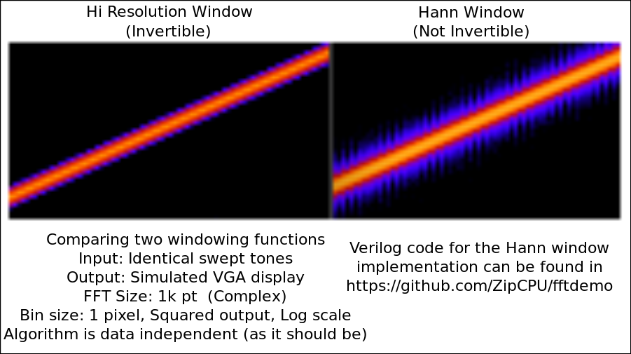
Perhaps the best way I could describe all of this would be to point out a spectrogram design I recently built. The simulation for this demo includes the A/D simulator I mentioned above, as well as the VGA output simulator. Using this simulation, I can capture any trace, and see every bit of logic flowing through my design as it reads from a (simulated) A/D device, filters and downsamples the signal, takes a Fourier transform, and then plots the result onto a window of my screen in a scrolling fashion.
If I want, I can then even test other signal processing approaches, such as the one shown below in Fig 4.
 |
This is what I mean by simulation: being able to repeat and test the entire design using software alone.
Further, all of these simulation components are available for student use (and more): they are (mostly) licensed under GPLv3. (Some are licensed under LGPLv3.) If your instructor/advisor allows you to, please feel free to try them and use them in one of your own projects.
Formal Verification
Since writing the original article on The Actual Design Process, I’ve come across a new technique so powerful when it comes to finding bugs that my own practices have since changed and changed significantly. Instead of first simulating any design components, I now formally verify every design component. I use this new technique in place of bench testing: it takes less work to do, finds bugs faster, and doesn’t require searching through GB of traces to find any bugs.
Why did I change? I changed because none of my bench tests ever tested enough of the design space. This meant that I would then integrate design components together that I thought were working, only to later discover the design as a whole wasn’t working.
Perhaps this would be during an integrated Verilator-enabled simulation. However, in that environment, I’d find myself searching through 1-10GB trace files trying to find a needle (the bug) in a haystack (the trace). Worse, I might’ve tried to place the design onto an FPGA where I no longer have the same visibility into the design in order to investigate any bugs.
On the other hand, when using a formal verification approach, such as the one enabled by SymbiYosys, I’d find (and fix) many more bugs than I would’ve ever dreamed of testing while trying to drive a simulation bench/test. Even better, I can normally find these bugs with between only 10-150 time-steps, and trace files less than 100kB in size.
Having used formal verification, do I still use simulation? Absolutely! Although I’ve discussed how to formally verify the aggregation of multiple design components, I have yet to learn how to do this reliably and in general with large system level designs.
That said, if you’ve never tried formal
methods,
then let me invite you to try out
SymbiYosys.
SymbiYosys is a free and
open-source program that can be used to formally verify a Verilog design.
Not only are there several example
designs,
in the SymbiYosys repository,
but you can also find examples in many of my own
repositories. Look in the bench/formal
subdirectory for any
SymbiYosys
scripts–those are the files that end in .sby.
Thank you for that excellent question!
Thou therefore which teachest another, teachest thou not thyself? thou that preachest a man should not steal, dost thou steal? (Rom 2:21)