
Bringing up a new piece of hardware -- what can go wrong?
For those who wonder what a “day in the life of” a digital design engineer might be like, let me offer the following account of “bringup week.” This is the week the team assembled, with all of their various parts and pieces, to put a hardware design together for the first time.
I’m getting ahead of myself, though, so let me back up a bit.
As background, I’ve had the wonderful fortune and opportunity to help build a SONAR system. Since I’m just a one-man shop, I’m only working on a portion of this system. My portion is simply the FPGA portion with some demonstration software thrown in for good effect. Others had developed and assembled the circuit boards, someone else had developed the actual SONAR circuitry, and another team had designed and built the transducers which would go in the water and couple the physical pressure waves with electrical signals. The digital board used to control this initial bringup effort was Digilent’s Nexys Video board–a very capable board for many reasons.
My job in this design was primarily two-fold: 1) command the SONAR transmitter, and 2) capture and save SONAR samples from the receiver. That was, and still is, the primary task.
As with any hardware project, there are several steps towards a working piece of hardware. The first couple of steps take place on paper. Then there’s an initial prototype design, where the parts and pieces get assembled together in order to test the concepts first placed on paper. Just before this step, I had picked up a Nexys Video board to test partial designs on. This is where I’ll pick up the story today–with the testing of this prototype design. Later, we’ll actually turn the component designs that formed this prototype into design components for a fully functioning SONAR system, with all of the ultimate functionality we are going to give it. But for now, we’re just testing our concepts with a basic prototype board.
Thankfully, most of the critical digital work was already done. I’d been working on the transmitter for over a year, and I was confident it would work. How could it not? I mean, the transmitter design logic was really simple. All I needed to do was to generate various tones, chirps, BPSK and/or BFSK waveforms. It was all very basic stuff. I say I was working on it for a year, but the original design was done in a day or two and I’ve only been tweaking it since then. As for the receiver, I was just planning on porting a receiver design from another project where it had already demonstrated the ability to work quite well.
Sounds pretty low key, right? I mean, all the stuff this project required was either really simple or had already worked before on another project. No problem!
Unfortunately, there were a couple big secondary tasks that didn’t come from other projects–not all of them explicitly written down. Worse, some of these were added into the requirements at a late stage of the game. Let’s go over a quick list of what new digital pieces were part of this design:
- Gigabit Ethernet
 |
Here’s the reality: we’re building a SONAR device. It’s going to get wet. That’s just the nature of this business. To make sure things can work in water, our plan is to seal all of the electronics into an air-tight can. Sealing that can will require a special technician, so … once sealed it’s not likely that I’ll see my FPGA board again. At that point, I’ll have only one interface available to my FPGA–and indeed to the entire device: a Gigabit Ethernet (GbE).
That’s it.
Think about this for a moment. There will be no JTAG port access to plug Vivado in to. There will be no serial port for debugging. There will only be GbE.
That means that any design problems, updates, or upgrades, must all be handled via GbE. Might you need an internal logic analyzer? You’ll need to configure it, read from it, and process it over GbE. Want to update the design? You’ll need to write a new design to flash and then command the FPGA to reconfigure itself all over GbE.
This sort of thing is often and typically handled via a CPU. What happens, however, when you need to update that CPU’s software? Similarly, what happens when the CPU software fails and needs to be debugged? All of that will need to be handled over the network.
For these reasons, I chose to handle several networking protocols in digital logic apart from the CPU–so I could have some confidence that they would continue to work even while the CPU was halted or being debugged. These protocols included the Address Resolution Protocol (ARP) and the Internet Control Message Protocol (ICMP, or “ping”), as well as the data packet protocol sending out the SONAR data and a debug protocol I built specifically for the purpose of being able to read and write addresses in the design across GbE without needing the CPU. That way, the network can be used to halt the CPU, read its registers, update its software, and more.
The good news is that I’d done projects with GbE before. The bad news is that this project will likely push the GbE to over 50% capacity. My previous approach to GbE was crippingly slow, and could never handle such rates. As a result, I rewrote much of it to handle AXI stream inputs and outputs so the hardware could do most of the network work automatically.
Hence, while the SONAR transmit and receive logic might be reused, the network logic contained a massive rewrite and a lot of new logic. The one good news to this new portion of the requirement is that we were only bringing up a prototype. The prototype wasn’t going to be sealed in a bottle, and so I still had the serial port and more available to me–with the understanding that future versions would remove this and any other excess interfaces.
-
Time Synchronization
Eventually, we’ll need to coordinate multiple of these SONAR devices together. That means they’ll all need to send their transmit pulses at the same time, and they’ll all need to sample the return waveforms at the same time.
Oh, and did I mention that any synchronization would need to take place over GbE?
As a bonus, I’m trying to figure out how I might synchronize these devices to GPS, but … I’m not there yet. Of course, there’s no GPS in the water, so the synchronization would have to come from above. The big difference would be that GPS allows you to do absolute time synchronization, vs the simpler relative time synchronization task of running multiple co-located devices.
Oh, and just to add into the mix: there’s no room in the one control cable containing the GbE connection to add specialized timing signals or even a common clock. It’s all GbE.
This logic is also new.
-
Audio
Somewhere along here, I must’ve decided that my task was too easy, and so I pointed out to other members of the team that the FPGA development board we were using for the prototype bringup had audio ports on it and asked if we could use them.
Well, okay, the story is a bit longer. The challenge with any test is that you need test equipment. How shall we know, for example, how much power the device is putting in the water if we can’t measure it? Measuring something like that requires a calibrated measurement device and I volunteered the FPGA as a way of reading from this calibrated device.
 |
I mean, why not use the I2S controller I’d built years earlier (and never tested) to listen to this calibrated device? The controller was already on board, it just needed to be read. Even better, if the FPGA read from the calibrated device, then we could have common time stamps between our transmitter and the calibrated receiver.
The other half of this measurement is the question of, how can you tell how good your receiver is? This requires having a known source that can transmit a known waveform, which can then be heard using the SONAR device under test. Basically, you need to be able to broadcast a waveform at a known volume and then receive at the same time. You can then take that received waveform, correlate it with the transmitted waveform, and get a measure of how much power you were able to receive. If you know how much power was actually in the water, you should then be able to estimate how much of that power you were able to successfully capture.
While we’re at it, why not just grab “sounds” from locations within the device to allow your “ear” to do some debugging?
 |
This is all well and good. My problem was that none of this was part of my original assignment.
An ugly corollary to the above problem statement is that I set up the audio device for 96k samples per second. The SONAR, however, was sampling at a much higher frequency. How than shall I take the SONAR, sampling rate and downsample it to the audio rate? Several of these audio sources needed resamplers, as shown in Fig. 3 above. Those also needed to be designed and tested.
-
Video
One of the hassles of our setup was that viewing the data was a challenge. By design, the prototype SONAR device would digitize sound waves from the water, assemble them into packets, and then blast those packets over the network. I then needed to write software to capture these packets and to write them to a file. The plan was then to read this file into Octave for analysis.
 |
The problem with this setup is that you don’t get any immediate feedback regarding what’s in the water. It takes time to capture packets, more time to read them into Octave, and even more time to then display these packets. Was there something that could be done in real time?
Well, yes. The Nexys Video development board we were using for this prototype also has an HDMI video output port. Why not use that to generate some canned displays? As it turns out, simple histograms, plots, and even falling rasters aren’t all that hard to build. Why not add these to the mix?
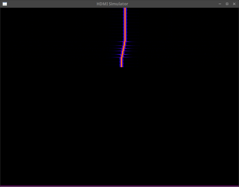
Fig. 4, for example, shows a falling raster. Recent time is at the top, and it scrolls down from above. Frequency goes from left to right, and the energy at any particular frequency is shown coming out of the page. (I.e. black has no energy, white has the most.)
In this case, the signal shown is a test signal for which I manually varied the frequency during a simulated test-run.
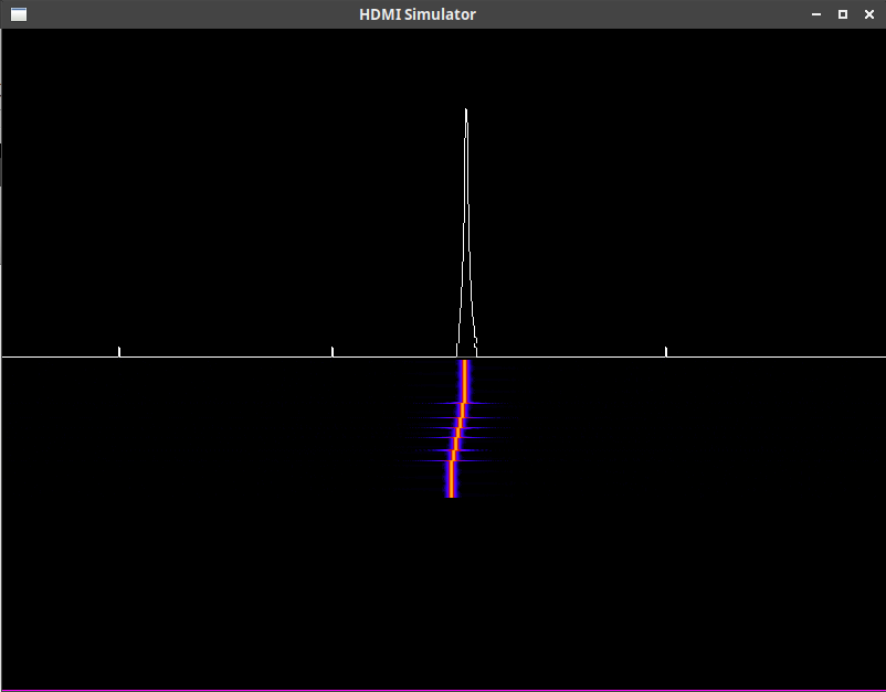 |
Fig. 5 is very similar, save that we’ve now split the screen in half using a blank video generator, plus two AXI video stream overlays in order to generate a split video. The top half shows a trace of the Fourier transform of the input signal, whereas the bottom half shows a falling raster again. Where the two meet, you can see the current Fourier transform and a horizontal line showing that spectrogram coming out of the screen.
So far, all this capability sounds wonderful!
That is, until it has to be made to work.
Remember, the most expensive part of digital logic (FPGA) design is not the design itself, but rather the verification of that design. Not only that, I had now permitted some major scope creep into the project. Neither audio nor video were ever required portions of the project. While I had done HDMI video before, I hadn’t done I2S audio nor had I ever configured the I2S chip I had using I2C before. (Remember my proposal for an ultimate I2C controller? This would be the first test of that controller.)
All this meant that there needed to be just that much more testing prior to bringup.
Programmatics
Just to add to the stress of the entire project, let me point out a very simple reality: It takes time to coordinate team activities. Put another way, if you want a design to work across the boundaries of multiple engineering teams, then you really need to get the engineers responsible for each portion of the design together into the same room and lock them in there until it works. That means there needs to be a time and date on a schedule for the meeting. Travel arrangements need to be made. This all needs to be done in advance, and .. it takes a lot of work to rearrange things if need be. No one wants to be the one individual responsible for telling the rest of the team that they have some problem or other and every one else will need to reschedule.
 |
On a larger project, we might have coordinated a “Test Readiness Review”, so that everyone would be on the record stating that their portion of the project was sufficiently working that the project was now ready for test. In our case, the analog engineer didn’t feel like he could debug his side of the board until he had access to a working digital design–forcing us to come together perhaps earlier than we might have otherwise.
Either way, once we put this bringup week on the calendar, it was then going to happen whether I was ready for it or not.
In my case, I felt like I was ready: I could simulate the device and see the critical portions of the design working nicely through all of the simulated digital hoops I had laid out for it.
Still, there was always the worst case scenario: What if my simulations were insufficient, or some hardware piece didn’t work like I had expected? What if I arrived at the test site and my stuff didn’t work? The last thing I wanted was to sit in a room full of engineers with everyone staring at me and asking me why my portion of the design, the digital logic, wasn’t working.
Preparation
Let’s just remember, though, I figured this task would be relatively simple: I already had the transmitter and receiver built, and the receiver had been used in another project. So … I allocated myself about two weeks to do my final preparations.
I suppose it’s not quite so bad as that. That’s just what it felt like towards the end. Looking over my git logs, I had the major portions of the design built and verified two months before bringup. They all built. They were all lint clean via Verilator.
My big problem, however, is that I didn’t have a large simulation infrastructure. I had a long list of things that should’ve been tested in simulation, but for which I didn’t really have a good model for. For example, my I2C model didn’t match that of the Audio chip I was going to control. Neither did I have a network simulation model (at first). I certainly didn’t have a model for the SONAR transmitter, and no method other than formal methods to verify it.
Still, I was confident things would work–perhaps naively so.
However, when I started building my design with Vivado I was quickly reminded of some of the limitations of Verilator’s lint capabilities. Sure, they’ve gotten a lot better since I last grumped about them, but Vivado still catches more wires that should be registers and registers that should be wires than Verilator does. (I know, Verilator is an open source project–I should submit a patch to fix these issues. I’ll just be honest and say that I haven’t done so–yet.)
 |
Then there was timing. Sadly, this design has way too many clocks in it. The SPI based A/D runs off of a 200MHz clock. The network runs off of two separate 125MHz clocks–one for transmit and one for receive. I would combine these two clocks, but there’s always the possibility that the network might not come up in GbE mode. In that case, the receive clock will run at either 2.5MHz (10T) or 25MHz (100T), whereas the transmit clock will remain at 125MHz. The audio runs off of a 24.5MHz clock. The rest of the design runs off of the 100MHz clock used by the DDR3 memory and exported by the MIG. That meant that, just to get the design to synthesize, I needed to write a lot of timing exceptions everywhere something crossed clock domains. Although tedious, the good news is that I found some places where I didn’t realize I was crossed clock domains, and all of those needed to be fixed.
One problem I had early on in when trying to implement my design centered around how to delay the network clock by 90 degrees from the data. My plan was to, and indeed my previous implementations of this interface did, output a clock using a hardware ODDR element, and to drive that element with a clock that was 90 degrees delayed from my data clock. As long as the two logic levels leading into this ODDR element were constant this shouldn’t be a problem, right?
Well, not quite.
There was always the possibility that the transmitter might need to run at a lower network speed than GbE, and then these values would need to toggle to generate a slower speed clock. But, my patience was thin, I just wanted it to work–not necessarily to work right. Unfortunately, Vivado gave me no end of grief trying to get timing closure using this method. In the end, I tore up that approach and simply output both clock and data using a 4x OSERDES. That way I could guarantee the phase relationship and clock crossings myself, and also guarantee that the network interface was done “right”. (Incidentally, I’ve also now verified–by accident–that the slower speed transmit mode works as designed.)
I was now ready to place the design on the board.
The first test? ARP and ICMP (ping). Why? Because if I ever need to debug a network connection, the first thing I always try is to ping the device on the other end. When you run ping on your local network, the first thing your computer will do is to broadcast an ARP request. Once it gets the response, and only then, will the actual ping packet get sent.
Neither worked.
I still remember that cold, depressed feeling as I stared at the board and wondered to myself, now what?
Unfortunately, I hadn’t put any debugging infrastructure into any of the new components of the design. I just … never thought things wouldn’t work. (You’d think I’d know better by now …) So my first step was to instrument as much of the network design as I could with Wishbone scopes. I started with the end points, and then worked my way towards the packet processors in the middle. Every step got a scope. It got to the point where I could touch any point in the packet processing chain to see what was going on.
Shall we look over some of the errors I found? Here was one: my packet miss counter wasn’t counting up the number of missed packets. See the bug?
	always @(posedge i_wb_clk)
	if (o_net_reset_n)	// See the bug?
		counter_rx_miss <= 32'h0;
	else if (rx_miss_stb)
		counter_rx_miss <= counter_rx_miss + 1;
If you missed it, just remember that _n is the suffix I use for negative
logic. The counter should be cleared on reset, and the test for that should’ve
been for !o_net_reset_n.
This wasn’t the only place where I got reset polarities mixed up. In a design filled with “working” and “formally verified” modules, you’d expect some bugs due to integration. Here was one of those bugs:
	pkt2stream
	icmp_stream (
		.S_AXI_ACLK(i_net_rx_clk), .S_AXI_ARESETN(rx_reset),//Same bug
		// ...
Incidentally, this was the exact same bug. rx_reset was active high, whereas
S_AXI_ARESETN is active low. Not only that, I found this same bug in a
couple of submodules of the same network control module.
Here’s another bug I found. Again, this is the sort of bug you might expect when integrating various “working” components together. In this case, I was using abortable AXI Streams, and needed a way to convert these streams to normal AXI streams that couldn’t be aborted and that could be written to memory if desired. (There’d be no room for TLAST in memory …) My method of handling this was to start each “packet” with a length word, followed by the packet payload. The bug? Well, the converter to AXI Stream calculated the length word based upon the length of the packet itself, whereas the bridge from a regular AXI Stream to an abortable AXI stream included the four bytes of the length word in its length count.
 |
Apparently, there was enough time separating when I wrote these two components that I forgot which format I was using. Then, to add insult to injury, neither of the two components using this format described the format properly in their comments. Had they done so, the issue would’ve been easier to debug.
Lesson learned: Document all interface formats.
 |
I also found a basic AXI handshaking bug in the packet merge utility. This utility, shown in Fig. 8, is responsible for granting channel access to one (and only one) packet source when that source wishes to send a packet. In my case, there were several possible packet sources: the ARP processor, the ICMP processor, the debug protocol handler, and the receive data processor. (Eventually, the list will include the network time handler and CPU packet handling as well.) In this case, the bug involved moving a data item forward in an AXI Stream when the slave was valid, rather than waiting for the slave to be valid and ready. The result was an extra word at the beginning of every packet.
Incidentally, this is one of those places where formal verification is no more complex than a counter: You count the number of stream words from a given stream’s packet input going into the mux, and you count the number of words coming out. Verify that the same number of words going in matches the number of words coming out. If you want to get fancy, you can even declare that word #XYZ (let the solver pick this) must have some solver chosen value, and then verify the same on the output. Still, the formal proof is quite easy to do. … You just have to do it.
During this whole process, I used Wireshark heavily to debug any errors. Wireshark could tell me, for example, if an ARP request was getting a response or not, or if that response had the correct format, or if not what part of the packet was in error. (Wireshark was also telling me that I was blasting packets of what looked like random data across the network–but we’ll get to that nasty bug soon enough.) If you ever find yourself doing network debugging, I highly recommend having Wireshark running during your debug sessions. The information it provides is just that valuable.
Once I had ARP and ICMP working, as well as seeing my receive data packets properly transmitted, I figured my task was done. I took a break and rested for the weekend. It wasn’t until the next week when I tried looking at the output of my ping command, and thus discovering that [ping](https://en.wikipedia.org/wiki/Ping_(networking_utility) didn’t think it was getting a response, that I dug even further down to discover that my IP checksums were all wrong.
Lesson learned: Wireshark doesn’t automatically check IP or UDP checksums. That functionality needs to be enabled.
Oops.
As it turns out, I had built my IP checksum logic based upon my memory of how the checksum was supposed to work from the last time I had built IP packets. Apparently, I had forgotten that the checksum needs to be inverted before use.
 |
By this point, I had also finally bit the bullet: I now had a GbE network simulation model. This model would send random ARP and ICMP requests, and validate their responses. It checked IP and UDP checksums. It would also validate UDP packets. Even better, I could send requests to my design via UDP on the local host, and the network model would then forward those requests into the design and then forward any responses back.
 |
This simulation capability was very helpful, and I’m not sure I would’ve found any of my remaining bugs without it.
Another ugly bug I wasn’t expecting was associated with adding packet headers and so forth to the design. In this design, the network engine accepts an AXI stream packet. That packet starts with the Ethernet destination and an EtherType (skipping the Ethernet source MAC), followed by any ethernet payload. Incidentally, this format helps keep all the AXI stream words formatted nicely on 32-bit boundaries–but that’s another story.
 |
It then fills out the rest of the Ethernet header, expands the packet to the minimum size (64 bytes), and adds a CRC. All of this extra “adding” process, however, takes cycles, and I wasn’t insisting on any dead time between packets to make sure these cycles were available. Rather, I had set the TREADY value associated with the incoming network packet stream to be a constant one.
Frankly, I never saw that one coming. Because I unconditionally set
TREADY=1, the network processing modules weren’t getting properly reset
between packets and so independent packets were getting merged together.
This wasn’t a problem with the previous design from which this one was drawn,
since the previous design used a different handshake to start packet
transmission.
Still, I figured I was at least close to ready.
I even had the network debugging port up and running. This port was a modified version of my serial port “debugging bus”, save that it had been modified to run “reliably” over UDP. Using this port, I could send commands to the device to read or write to any address found within my FPGA design. The basic protocol was that the external computer would send a packet to the FPGA requesting a bus transaction, and then wait for the FPGA’s response. Every packet was given a response. If there was ever no response, the request would timeout and then get repeated. As a result, no more than one request would ever be in flight at any given time–although there might be multiple copies of that one request and its response in flight. To handle that, if the FPGA received duplicate packets, it would only run the bus requests once for the first packet request, and then simply repeat the response it had generated for that request on any subsequent requests. No, the protocol wasn’t very efficient networkwise, but it was MUCH faster than the serial port it was replacing.
Now that I had all of this working, it was time to start staging for the trip.
Staging
“Staging” is my word for separating all of the hardware that will be traveling with me from my fixed development environment. My desktop would not be traveling with me, so I needed to bring a laptop–and a newly purchased one at that. That laptop would be a special project laptop. It needed to have Linux installed, Vivado, Verilator, GtkWave, Icarus Verilog, zip-gcc and … all my favorite development toys. Once I had all these installed, I cleared off a table and started setting up my traveling equipment.
Of course, once I put it all together, nothing worked.
Sound familiar?
This time, it took me almost a whole day to chase down the problem. (I hadn’t allocated time for this extra day …) Apparently, that brand new laptop I had just bought for this trip and this project came with a bad Ethernet port. (Or had I broken it somehow? I’ll never know …)
The problem with this was, I had assumed everyone else’s hardware “just worked.” Had I suspected the laptop might have a bad Ethernet port, I might’ve saved myself a half day or more by trying my USB to Ethernet dongle earlier.
Instead, I turned to my (working) MDIO controller for the first time only to discover … it wasn’t working. I couldn’t figure out what had happened. I knew the design worked before the last time I used it, but somehow it wasn’t working today. In particular, the bits returned were off by one, and the last bit wasn’t trustworthy. In hindsight, looking over the design with gitk, it looks like I had tweaked this design since copying it from the “working” project and … not validated it since. Those “tweaks” were what wasn’t working.
At this point, though, I was less than a two days out. It was now Wednesday, the train left on Friday, and I had only just gotten my tests running again in this staging area. Then, when I went to double check everything again, I discovered that … the SONAR data packets weren’t getting through anymore.
At this point, I was out of time. I had a critical capability that wasn’t working, but it was now time to pack up all my hardware for the train. (I swear it was working earlier! What happened?)
 |
The Train
Let me set the stage a bit more for what happened next.
The SONAR data processing in this system takes place in several steps:
-
All of the digitizers for the various sensors sample their data from an SPI based A/D concurrently.
-
That data is then serialized, and organized into blocks of 24 samples, with 24-bits per sample.
-
Each block is then examined to calculate an appropriate block exponent.
-
The samples are then compressed into 16, 20, 24, or 32-bits per sample.
Okay, so stuffing 24-bits into 32-bits isn’t much of a compression, but it does make it easier to examine what’s going on when staring at a hex dump of the packet.
-
Finally, the samples and exponents are assembled together into packets of 32-bit words. The packets contain configuration information, the time stamp of the first sample, possibly some non-acoustic data, and then transmit information is appended to the end of the packet.
This takes place in a module I called
rx_genpkt. By the time I got on the train, this module had just recently been formally verified (we’ll discuss that with Fig. 13 below), and no longer showed any signs of being broken in either simulation or hardware. -
Ethernet, IPv4, and UDP headers are then added to the sample packet, containing the length of the packet, IP and UDP checksums, and so forth.
This takes place in a module I called pkt2udp, the one module I knew was broken when I got on the train.
-
The packet then gets multiplexed between the SONAR sensor data source and a second (microphone) data source–following Fig. 2 shown above.
-
It then crosses from the 100MHz to the 125MHz clock domain.
This clock domain crossing component is really nothing more than a traditional asynchronous FIFO. The “packet” getting placed into this FIFO consisted of a 4-byte header containing the packet’s length, followed by a payload containing as many words as were required to capture the rest of the number of bytes requested in the header.
-
Once in the 125MHz domain, the length word is stripped from the packet, and the packet payload is then broken down from 32-bit words to 8-bit octets.
The 32-bit word size turns out to be convenient for both assembling the packet, as well as making sure that packet generated using a 100MHz clock can keep the network busy on every clock cycle of a 125MHz clock.
-
Finally, the packet goes through an arbiter that selects one packet request at a time, from among several potential packet sources, to forward to the network core.
-
The network core then adds a MAC address. (See Fig. 11)
-
The network core then pads the packet to a minimum of 64 bytes
-
A CRC is then added to the end of the packet, and
-
A preamble is added to the beginning of the packet.
-
The packet then travels the network.
In general, there’s one module for each of these steps, and most of these modules have been formally verified. There were two notable exceptions to this rule.
The first exception was that the initial packet assembly, where we added configuration information and timestamps. Just before I left, I had narrowed down a bug to this logic, as shown in Fig. 13 below.
 |
At the time, this packet assembly logic wasn’t located in a separate module but rather in a module containing other modules. As such, it hadn’t been formally verified. Just before leaving, I had traced a nasty bug to this module, as shown in Fig. 13 above. That was enough to split the remaining processing logic into a separate module for formal verification. Once separated, this processing module then became easy to verify.
Unfortunately, the bugs in the RxCHAIN weren’t the last bugs in the system.
Another bug appeared in pkt2udp. Once I had formally verified (and fixed)
the receive chain, this pkt2udp module was the only one left in the chain
that hadn’t been formally verified.
What did pkt2udp do? This was the component responsible for turning a
sensor data packet into a
UDP packet.
Frankly, I didn’t trust this module at all. It felt like I kept tracing bugs into the module, but could never find their cause.
 |
For some more background, understand that this component’s operation centered around the circular buffer, shown in Fig. 14 above. (A ping-pong buffer pair would’ve been easier to verify.) Within this buffer, the first 32-bit word of every packet in the buffer was to contain the length of the packet that would follow.
Writing to this buffer meant:
-
Clearing the packet length field. This was usually done as part of writing the previous packet to memory, but on reset it might need to be cleared manually.
-
Write data into the buffer, counting how much data gets inserted
-
Abort (drop) the packet if 1) the source aborts aborts, or 2) if the one packet uses (or will use) the entire memory buffer.
-
Once the packet is complete, write a zero to the field following. This will become the length field of the next packet.
-
Then go back and write the finished packet length into the buffer
-
Finally, move the write-packet boundary forward in the buffer. Our packet has now been committed to the output stream. It now has a reserved location in RAM. It won’t be dropped from this point forward.
The key to all this processing is the length field. A zero length means there is no packet present. Once a packet was committed, the length of that (now committed) packet would be updated in memory once we guaranteed that the next packet’s length field was set to zero.
If at any time during this process there wasn’t enough room in the buffer for the packet, the packet needed to be dropped. There were two parts to this. First, if the packet filled the entire memory and there still wasn’t enough memory to finish the packet, then the packet would be dropped internally. The source would never be the wiser. This keeps the routine from locking up on an over-long packet. Second, the incoming packet would stall if the writer ever ran out of memory between the write and read pointers. If it stalled for too long, the packet source might also abort the packet–once it couldn’t stall any longer. (Remember, data is coming in at a constant rate. It must either go somewhere, or get dropped if the system can’t handle it. You cannot stall indefinitely, neither can we allow partially completed packets to move forward.)
The read side of this process was simple enough as well: You’d read from the first word where the last packet left off. While that word read zero, the reader would stay put and just keep reading that length word. Once the length word became non-zero, the reader would start reading the packet out, by reading and then forwarding the packet’s data.
I’m sure most of you will recognize this structure as a basic linked list. The biggest differences between this linked list and the ones you find more often in software are 1) the wrapping memory, and the fact that the “pointers” in this case were lengths, rather than true pointers, and 2) in hardware, you have to deal with timing and timing cycles. These are minor differences, though: it’s still a basic linked list: the first word in a packet gives the packet’s length, and therefore points to the first word, the length word, in the next packet.
Indeed, the operation of this IP is all quite straight-forward, but I had no end of trouble with this design. It got so bad at one point that I even (gasp!) built a Verilog simulation to bench test it. That bench test was really hard to get right, too. I spent a half day toggling between assuming that the reader would accept packets out at full speed, or that it would accept them at quarter speed, only able to get one of the two speeds working depending on how I set the M_AXIN_READY input. While I eventually found that bug, it wasn’t really enough.
What the design needed was to be formally verified.
Why wasn’t it formally verified? How was it that I had gone so long without formally verifying this critical component?
The simple answer is that I couldn’t figure out how to go about formally verifying a linked list.
As a result, I was now on an Amtrak train headed for hardware bringup with a known bug in my digital logic design. Using my own internal logic analyzer, I had caught this bug in hardware just before leaving. What I discovered is illustrated in Fig. 15 below.
 |
I should point out that I only discovered this via the internal logic analyzer. I’m not sure I would’ve known where to look without it. While the internal logic analyzer told me where the design was stuck, however, it didn’t tell me how it got stuck in the first place.
Here at least I knew that, due to some unknown condition, the read pointer would be reading a zero length packet somewhere in memory (meaning that there was no packet present), all while the write half of the module was working on a packet elsewhere. The design would be locked up, never to go again. However, while I could discover this much using my scope, I couldn’t figure out how the design ever got into this configuration. This wasn’t supposed to happen!.
Therefore, on the train, I decided to try the following approach to formally verifying this linked list chain:
-
I would allow the formal tool to select two arbitrary memory locations.
-
I would start tracking these two locations as soon as the first location pointed to the second one. If it never pointed at the second location, I’d never track what happened next.
A formal-only state machine’s state register would note that I was tracking a packet existing between these two pointer addresses.
-
I then tracked these two addresses, and their values, until the read pointer pointed at the first of these two locations, so that it would start reading out the packet. Frankly, I didn’t need to go farther: I had the read tracking logic working in my formal proof already. I just needed to get to this point where I could guarantee that the read pointer would be given the right data.
-
I also formally verified particular properties of these two locations: 1) The first address, plus the length contained at that address, had to point at the second address. 2) The writer could be active starting at the second address, but never between the two. 2) The packet length was at least a minimum packet length, and always less than the full memory size, and so on.
-
For all other linked list pointer-pairs within the design that the formal tool might encounter, I assumed these properties.
Once I had this plan in mind, I was then able to formally verify the packet to UDP module. What I discovered was a strange corner case: If the source aborted the packet just at the exact same clock cycle that the UDP packet assembler completed it, a zero length word would be written to the packet’s length word, and the writer would move on to the next packet.
Just to see what’s going on, here’s what the original packet assembly logic looked like:
	always @(posedge i_clk)
	begin
		case(state)
		// ... assemble the parts and pieces of the packet together
		endcase

		// On either an external or internal abort ...
		if (S_AXIN_ABORT || abort_packet)
		begin
			// Write the null pointer back to the first address
			// of memory
			mem_wr <= 1'b1; // Write to memory
			mem_waddr <= next_start_of_packet;
			mem_wdata <= 0;

			state <= S_IDLE;
		end

		if (!S_AXI_RESETN)
		begin
			// Reset stuffs
		end
	end
The problem here is, what happens if the packet is already fully assembled when the abort signal is received? We were then going to write the length of this packet and set the packet start address to the next start of packet address. The abort condition would override that write, causing us to write a null pointer which would then cause the reader to freeze waiting.
And here’s the corrected condition:
	always @(posedge i_clk)
	begin
		case(state)
		// ... assemble the parts and pieces of the packet together
		endcase

		// On either an external or internal abort ...
		if ((S_AXIN_ABORT && state <= S_PAYLOAD) || abort_packet)
		begin
			// ...
Notice how, this time, the packet is only aborted if it hasn’t been completed. That is, we don’t abort after we’ve received the full payload of the packet. Once the payload has been completed, we do nothing more with the abort logic.
In the end, it only took between 4-6 hrs on the train to fully verify this packet to UDP bridge. That’s 4-6 hrs compared to the last several weeks where I was dealing with this bug on and off depending on the conditions within the design, depending on when the hardware switched from 10Mb mode to 1GbE mode, and so forth. Worse, during those weeks, I could never quite pin the bug down to one module, so it really required formally verifying everything else to get to the point where I could isolate this bug to this module.
Now, at least, I had found the bug. Even better, I now had confidence that this last unverified portion of my design would work as intended. I just had nowhere to assemble the hardware to test it until the team was assembled on Monday morning.
Bringup Bugs Found
So, once Monday morning came around, I joined the team at the test site. I plugged in the hardware and my newly verified packet to UDP converter “just worked” like a champ.
Instead, I had two other bugs to deal with. (These weren’t the first bugs of the day, either–those were in the circuitry elsewhere and not my digital logic.)
The first was associated with a weird corner case. The network hardware is designed to start up in 10Mb Ethernet mode. It then senses whether or not the cable is capable of 100Mb or 1Gb Ethernet. Once that sensing is complete, the network hardware will switch modes. My design, however, only checks and changes speed between packets.
What happens, then, when the SONAR receiver starts assembling data into packets and then attempts to blast so much data across the network that there’s never a rest between packets for the network controller to use to change speed in?
What happens is that the network controller gets so stuck that the debugging packets can’t get through. Without the debugging packets, it was impossible to send (via the network debugging port) a command to halt the packet generation. It’s a classic chicken-and-egg problem.
For the time being, I could get around this bug easily enough by turning the receive data handling off (via UART), letting the network adjust, and then turning it back on again. By the Tuesday morning (Day #2) I had a more permanent fix for this in place, whereby the data packet generation wouldn’t start until the network was in high speed 1Gb/s mode. Indeed, after the second morning, I never needed the UART debug bus backup port again–it was all network control after that.
It was the second problem that was more of a hassle that first day.
For background, remember that this is the first time my FPGA logic was connected to hardware on this project.
 |
When the receive processing logic was first checked out years ago, I had two potential test sources, as shown in Fig. 16.
The first was an emulated A/D inside my design, which I could use as a source if I needed one and had no hardware. This emulated A/D consisted of a series of CORDICs, each generating a sine wave at a different frequency and amplitude, but all of them phase aligned. The result was then encoded appropriately to match what the A/D output would be–it became the “MISO” input from an emulated A/D. As a result, if you ever plotted the receive waveform from this artificial test source, you’d see some easily recognizable signals.
For this project, however, I had decided that the emulated source was probably overkill.
Instead, I used the second test source configuration in the A/D controller. This test source would replace whatever was actually read by the A/D with a counter and the channel number. I could then follow this incrementing counter through my processing chain to make certain that no data was ever dropped. This project now marked the second time I’d used this counter approach. The first time, on the original receiver project, I automatically verified that there were never any breaks in the counter when the results were finally received by the software processor. This time, however, I just looked at a couple of packets in hex, by eye, to verify there were no packet breaks.
So, now, with the whole team assembled, we connected a signal generator to the A/D input. The histogram of the output looked wonderful, so I figured everything was good–up until we all looked at the waveform. Instead of a sine wave, we got something like Fig. 17.
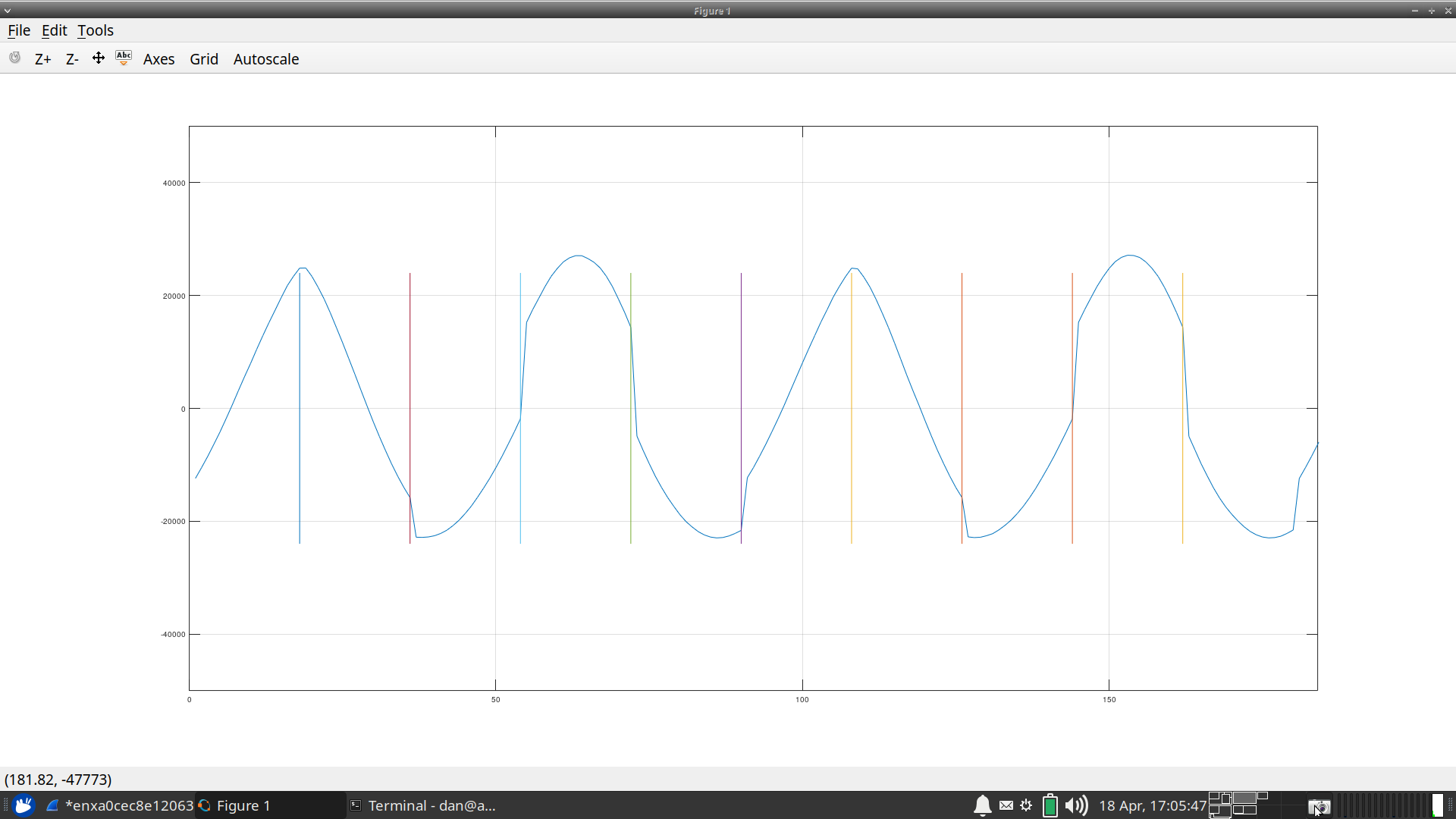 |
In this figure, you’ll notice discontinuities in the sine wave. As a hypothesis test, I’ve placed vertical bars every 18 samples. You’ll notice that these vertical bars land right on those discontinuities–every 18 samples.
At one point, we tried increasing the amplitude. We got something worse, as shown in Fig. 18.
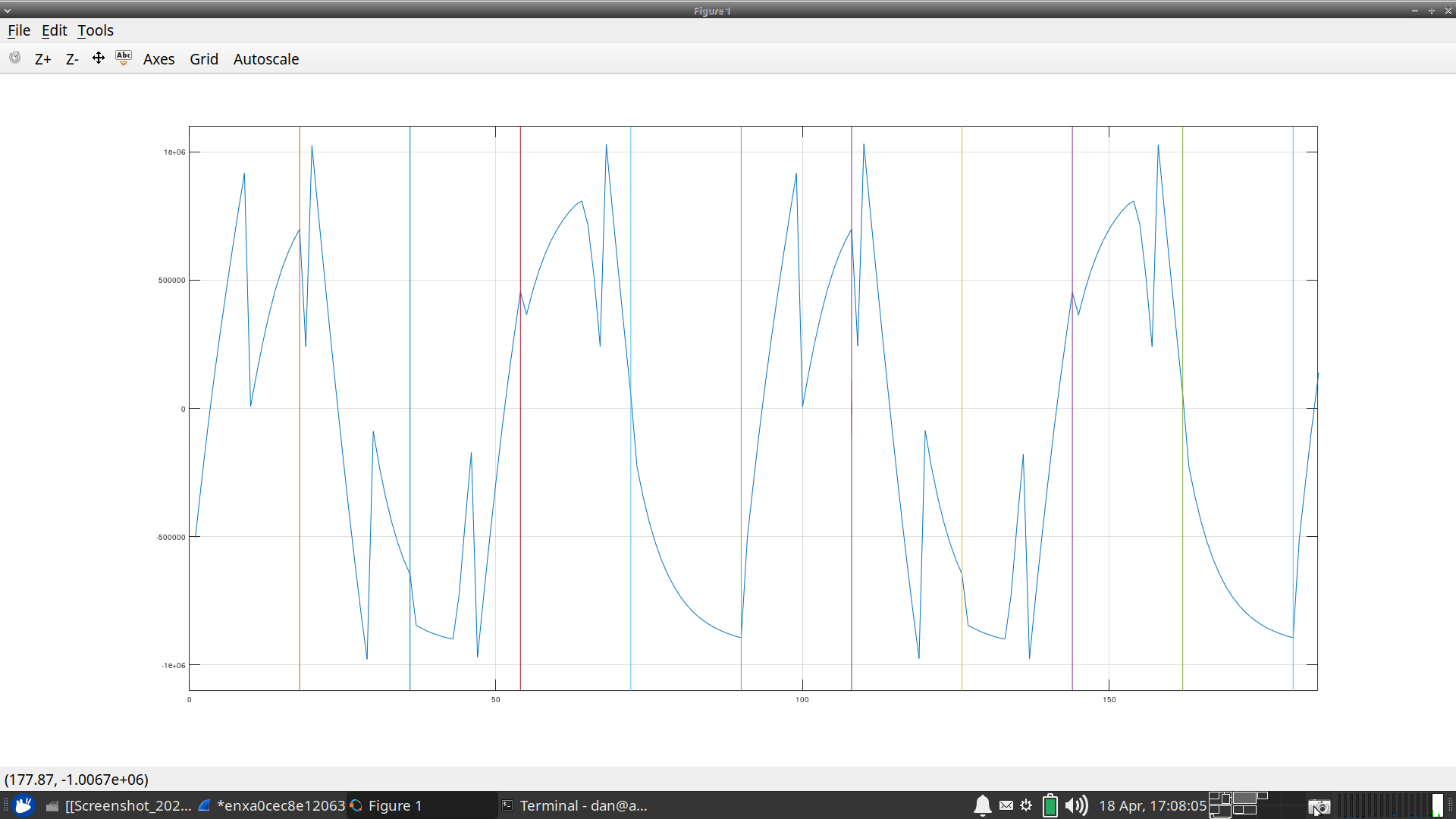 |
Let’s start with what we know. Sudden breaks in what should be a smooth waveform sound like samples that are getting dropped somewhere. So, I checked for lost samples. I turned on the counter injection at the source, as shown in Fig. 16, and then had my packet software dump the data in hex so I could check for lost samples.
There were no lost samples.
I was confused. That first day of testing ended in frustration.
On my way out the door, however, another teammate suggested based upon the frequency we were measuring that I was dropping exactly 6 of every 24 samples. As it turned out, that was just the help I needed to find the bug.
Surprise! The dropped samples bug wasn’t in my hardware at all.
The network packets were arriving at their destination without error, and without any dropped packets. I had verified by eye that nothing was getting dropped. That wasn’t the bug.
No, the bug was in my latest rewrite of the packet handling software, the
same software that both collected packets and converted them to a text file
so that Octave
could ingest them. As of the latest rx_genpkt rewrite, I had run out of
meta-data room to stuff the number of samples per packet in the header.
Instead, the software would simply know this value as a shared
constant. My problem was, when re-writing this software, I looked up the
packet size from a VCD
trace, shown in GTKWave, and generated via
simulation
just to be sure I got it right. I read
that there were 0x18 samples per packet, and then wrote the software to read
out 18 samples per packet–dropping six samples from every data packet in the
process. (Did you notice the accidental hexadecimal to decimal unit change?)
That fixed the discontinuities in Fig. 17. What about the additional discontinuities in Fig. 18? Those discontinuities came because, surprise, surprise, I was now using Xilinx hardware instead of ~ALtera~ Intel hardware. I had also changed the front end. The receive wavefoms were running though some IDDR elements and there was an additional delay in when the MISO were returned to my controller. As a result, I was sampling the bits from the A/D on the wrong clock cycle. This was easily found (and fixed) using my internal logic analyzer. I’m not sure how I would’ve found this delay otherwise.
Needless to say, by Tuesday morning I had a parameter in the design allowing me to adjust the capture delay by eye, and I was able to adjust it so that it now captured in the center of the bit.
Fig’s 17 and 18 show one more bug in them, most obvious in Fig. 17: the sine wave wasn’t uniformly smooth between its positive and negative half sides. This one wasn’t my fault. Instead, we traced it to a mis-configuration in the function generator we were using to generate the sinewave in the first place. We had it set to clip the negative half of the waveform–although this was more obvious when we ran a triangle wave through the system (not shown above).
These three bugs ended up being my last show stopping bug for the week. The rest of the week everything I had written “just worked” like I wanted. (Don’t worry, we’re not superhumans, we still had other bugs to chase down … there just weren’t any more of them in the digital logic. Or, to be more exact, there weren’t any more bugs in the digital logic that any one else noticed.)
Sudden New Capabilities
There’s one more story worth telling from this week.
As I’m sure you can imagine, this being the first time the team was assembled, things didn’t go as smoothly as everyone had planned. I wasn’t the only engineer in the team with faults that needed to be chased down. In particular, we were chasing down some hardware faults in the transmitter on Thursday. Things weren’t working, and we weren’t certain why.
The team then asked me if it would be possible to transmit from only one of the transmitters on this device.
That wasn’t a request I was expecting. Nowhere in the requirements did it say that I needed to be able to transmit onto a selectable subset of the transducers controlled by the device.
In general, adding a capability like this sounds pretty easy. All you need to do is to take the output data and mask it with a register telling you which transmitters are “on” and which ones are not. The fix, in Verilog, was just about as simple as inserting the following lines of logic.
	generate for(gk=0; gk<NUM_SONAR_ELEMENTS; gk=gk+1)
	begin : ADD_ENABLES

		initial	o_tx_control[gk] = 0; // This is an FPGA, initial works
		always @(posedge i_clk)
		if (!tx_enabled[gk])
			o_tx_control[gk] <= 0;
		else
			o_tx_control[gk] <= int_tx_control[gk];

	end endgenerate
That was the easy part.
Now let’s put this problem into a broader context: This design has a ZipCPU, memory, many controllers, scopes, etc. Every peripheral within the design has its own address assignments. There’s also an interconnect, the responsible for routing requests from their sources to the peripherals being referenced. Putting something new like this together will require allocating a new address for a new peripheral register. That peripheral will then need to be added to the interconnect, the interconnect, will need to be reconfigured for the new address map, and then all the software will need to be adjusted for any addresses that had to change during this process and so on.
That’s a lot of work.
Oh, and did I mention I wasn’t using Vivado’s IP integrator? Nor was I using their AXI interconnect? (I was using Wishbone. I could’ve used AXI, I just chose not to.)
Using AutoFPGA, we had all this work done in less than a half an hour. When you consider that Vivado took about half of that time for synthesis and implementation (I wasn’t counting at the time), this may be even more impressive.
Audio and Video
In the end, neither the brand new audio nor the video capabilities were tested during this bringup week. That’s kind of a shame, so I figured I’d at least discuss some pictures of what the video might look like in simulation.
Fig. 4, back in the beginning of the article, shows one such falling raster. In this figure, frequency goes from left to right, and the displayed image scrolls from the top down. The source is an artificially generated test tone, generated internal to the system. At several points during the simulation, I adjusted the tone’s frequency, and you can see these adjustments in the image.
Similarly, Fig. 5 shows a split screen, with a trace on top and the falling raster below. Note how the frequency axes are identical, so that the trace sits nicely on top of the raster, with the raster showing how the trace had adjusted over time.
I suppose it’s a good thing the video outputs didn’t get tested. They didn’t work in simulation, until the end of the week. Below, for example, is a bug that locked up the Video source selector. (Remember, I had five video sources, each generating video signals, and so I need a selector in the system somewhere to select between which one would be displayed.)
if (!VALID || (HLAST && VLAST))This was just a basic AXI bug. The correct condition should have read:
if (!VALID || READY)This is just a basic AXI stream handling rule. I should’ve known better, and so I’m kicking myself for having made it. The good news, of course, is that this bug was easily found with just a touch of formal methods.
Perhaps I’ll have a chance to show off these (now working) video capabilities during our next hardware test.
Conclusions
So, what can we learn from the week and the preparation leading up to it? Let’s see if we can draw some conclusions.
-
Expect failures–even in hardware. Plan for them. Give yourself time, ahead of time, to find and fix failures.
While it sounds weird, I like to put it as, “Fail early, fail often.”
-
Simulate all major interfaces! I lost a lot of preparation time believing that my network interfaces “just worked”, simply because I hadn’t bit the bullet and built a proper network simulation model first. Once I had that model, debugging the network got easy, and my bug-to-fix times got a lot faster.
-
For all of my simulation work using the packet to UDP converter, nothing managed to catch the actual bugs I was encountering in hardware. I would’ve had to trigger the abort on just the right input sample to trigger this, and I had no idea (before finding the bug using formal methods) how I might’ve set up the simulation to stimulate the bug.
-
It’s a lot easier to find bugs using formal methods than it is to find them in hardware.
-
Frankly, if it’s not been formally verified, I don’t trust it. Remember Fig. 13? The last two items in that processing chain to get formally verified were the last two items with bugs in them. Of those two, the one item that was the hardest to formally verify turned out to be the last item in the design with a difficult bug to chase down. Once formally verified, however, it worked like a charm.
This isn’t to say that every formally verified module worked the first time. Rather, not every formal proof I ran was sufficient to guarantee proper functionality the first time. The proofs got better the longer I worked with each of the individual components of the design.
-
Yes, it is possible to formally verify a linked list. I wish I had formally verified the pkt2udp module earlier–it would’ve saved me a lot of head scratching during the weeks leading up to my travels.
-
Document your interfaces!
-
The sooner you move to the “staging” area, the sooner you can debug your chosen travel hardware.
-
Plan early on for how you will debug a design. Adding the (unused) Audio and Video capability into the design late in the game took a lot of my time and – we never got to testing either of those interfaces. (We might’ve started testing with them sooner, if I arrived with more confidence in their functionality–but that’s another story.)
-
With a little focus, you can get a lot of work done on Amtrak’s auto train, while still bringing whatever hardware you might need.
-
While I didn’t discuss this one above, here was another lesson learned: If you have a complicated condition, and two or more things depend upon it, create a common signal to capture that condition for both pieces of logic. In my case, I had a condition for when a received packet should be generated. That condition was repeated in two different locations of the same module. Among other things, it checked how much space was available in the buffer. I then updated the condition to help guarantee sufficient space was available, but only updated it in one location–not both.
This was the bug in Fig. 13, and one I found when I finally formally verified the data packet generator.
-
Looking over all the bugs I found, I seem to have traced several to the boundaries between formally verified components–at a place where things weren’t verified. I’ll have to think about this some more.
-
Finally, while I can be critical of others making basic mistakes, I made plenty myself. I think the worst one I found was checking for
!VALID || VALIDwhen what I wanted to be checking for was!VALID || READY.
Let me leave you with a final thought from the first verses of Psalm one, a Psalm I’ve started to make a habit of reciting to myself on trips like this one:
Blessed is the man that walketh not in the counsel of the ungodly, nor standeth in the way of sinners, nor sitteth in the seat of the scornful. But his delight is in the law of the LORD; and in his law doth he meditate day and night. And he shall be like a tree planted by the rivers of water, that bringeth forth his fruit in his season; his leaf also shall not wither; and whatsoever he doeth shall prosper.
May God bless you all.
And unto Adam he said, Because thou hast hearkened unto the voice of thy wife, and hast eaten of the tree, of which I commanded thee, saying, Thou shalt not eat of it: cursed is the ground for thy sake; in sorrow shalt thou eat of it all the days of thy life (Gen 3:17)