
Using a Histogram to Debug A/D Data Streams
My favorite part of any signal processing application is the part where you sit down and draw out what you’re going to build. It’s my favorite part because nothing ever goes wrong on the drawing board.
 |
But let’s face it, things do go wrong, and you are going to need to be able to find out what.
One of my themes in this blog is that you should prepare, early on in any project, for the tools you will need to accomplish that project. For example, you should build and prove your debugging bus early on. Then, later on, you can use this ability to communicate with your design while it’s in the lab so that your design can tell you what’s going right or wrong.
In this game, logic is your friend: use it.
That said, let’s take a quick look at four things that can be quite helpful when trying to go from an signal source to your data processing application:
 |
-
Sample counting
Sample counting should be your first step, before everything else. Sadly, from my own personal experience, adding an internal data sample counter has tended to be an afterthought that ends up getting placed into every project only after things start going wrong. Typically, the A/D isn’t properly configured, the internal clocks within the design aren’t set right, that resampling filter didn’t quite get the rates right or maybe something else.
Counting samples, and comparing the incoming sample rate to the system clock rate can be very valuable when trying to narrow down the source of your lack of data, or even when trying to find where samples are getting dropped (or added) into an application.
 |
-
Counter injection
Often there’s a long path with lots of things on it going from the digital signal source to output data. In one of my early projects, this path included packing data into words and then writing it to an SD card only to be read later. In another project, the data needed to be first given an exponent, then packed into blocks, placed into a FIFO, and sent over the Ethernet.
Even though none of these steps involved any filtering or control loops, there were still a lot of places where things might’ve gone wrong. As an example, in the SD card project, the SD cards we were using would tend to become busy mid-stream and so drop samples whenever our FIFO didn’t have enough depth within it. (Worse, we were using an extremely small, low-power design to record a GPS signal that couldn’t afford data loss. Because the chip was so small, there wasn’t much block RAM available for a deeper FIFO. Yes, it was a recipe for a project failure. In the end, we needed to get creative to get around this bug …)
One easy way to diagnose problems like this is by injecting a counter into the data path. You can then compare the counter against the signal on the other end of the transmission to verify that nothing was lost in the FIFO, that the SD card didn’t skip samples any where, that no network packets were dropped, or worse.
This is such a valuable capability to have, that I’ve often placed it into every signal source controller I’ve built.
-
Histogram checking
This is going to be our topic today, so let’s come back to this in a bit.
-
Fourier Transform
Finally, when the samples all look good, it becomes time to go look at a Fourier transform of the incoming data. I personally like the Short-Time Fourier Transform (STFT) the best. A nice rastered image, presenting the STFT of your data can reveal a lot of what’s going on within. You can see if there’s some bursty noise, what sort of always-on interferes might be coming in from your system, whether you are struggling with self-noise and more. Indeed, this is a very valuable analysis step–it just doesn’t tell you much if your signal was corrupted earlier in the processing chain, and your samples were replaced by something else.
As an example, I’ve worked on many signal processing systems that were buffer based. In these systems, you’d process one buffer, then get the next to process it. Very often, filtering implementations would require overlap between the buffers. A common problem was always making sure there was no dropped (or inserted) data between the buffers. The counter injection check above could find this easily. However, if you skip the counter injection check and instead go straight to taking an FFT of the broken data, then you may well convince yourself you have a wideband interference issue after which you’ll then go looking in the wrong place to find the source.
Today, though, let’s look at how a histogram might help you diagnose data sampling problems, and then look at some examples of how you might implement a histogram in an FPGA.
The Power of a Histogram
A histogram is defined as a chart of sample counts, estimating the probability that an input voltage will get mapped to a particular digital value. If done well, it should approximate the probability distribution of the underlying data source.
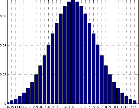 |
A classic example of what a histogram might look like is shown in Fig. 4. on the left.
You should be able to recognize this shape as a Gaussian bell shaped curve. It’s the distribution you should expect from thermal noise. If everything goes well, this is what you should see coming into your system when everything is working but no “signal” is present. In other words, this is what things will look like before you turn your transmitter on.
What’s even better about this picture is that, since a histogram is a visual picture, it’s easy to tell from a chart whether or not what you are receiving matches this shape. Pattern recognition is very powerful.
 |
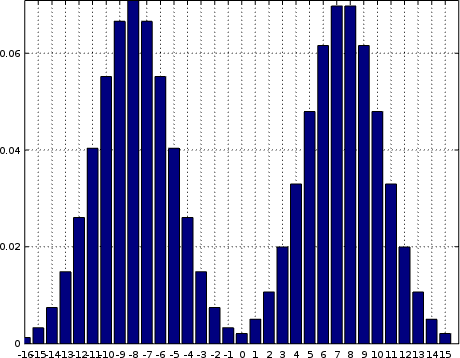
So, if that’s what a histogram of noise (i.e. no signal) should look like, what should a histogram of some form of signal look like? Fig. 5 on the right shows the histogram of what you might expect from a sine wave under the uncommon laboratory conditions of pure signal with little noticeable noise.
Unlike the Gaussian histogram, this one looks more like Batman’s head as I term it. Notice the pointy “ears”, beyond which there’s no signal counts at all. In a perfect world, this is what your histogram, of noiseless signal should reveal.
Of course, we don’t live in a perfect world, and so I’m not sure I’ve ever seen a histogram looking this clean generated by anything other than a digital NCO that never touched the analog domain. So what should this histogram look like if your sine wave has been corrupted by some amount of Gaussian noise?
Unfortunately, the probability math starts getting really complicated when combining signals. For example, adding a Gaussian to a sinewave in time results in a convolution of the two probability distributions functions. For anyone who wishes to try to evaluate this convolution, good luck–the math can get quite challenging.
 |
For the simple minded like me, it’s worth knowing that convolution with a Gaussian acts like low-pass filtering the Batman head, smoothing over those sharp “ears”. As a result, with a bit of noise, your signal might look like Fig. 6 on the right.
This is what you should hope to see when evaluating a signal from an A/D: either a nice Gaussian when no signal is present, or a smoothed Batman’s head when it is. Well, that or something else depending on how your signal is defined. It shouldn’t be too hard to figure it out in Octave.
But, what else might you see?
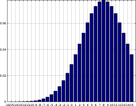 |
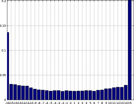
Two very common problems in A/D systems are bias and scale problems. Fig. 7, on the left, shows what bias might look like. This particular signal was generated from a Gaussian with a non-zero mean, and represents much of what you might receive if you had an input of both electronic noise added together with some amount of direct-current leakage onto your signal path. Note how the signal is no longer symmetric about zero.
Okay, I’ll admit to the purists here that I cheated when drawing Fig. 7. I used Octave and a theoretical bell shape shifted to the right. The result is pretty, but practically erroneous. Specifically, the far right bin should also include all of the counts from samples that ended up out of range.
 |
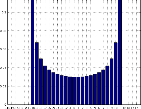
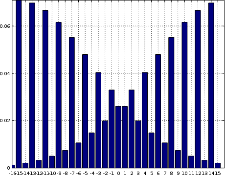
Speaking of “out of range”, the second common problem you might have is scale. Many receivers require some form of gain prior to going into the sampler. Getting the right amount of gain can be a challenge. As an example, Fig. 8 on the right shows what might happen if you overdrive the incoming signal. Yes, take that headset off quickly before you lose the last of your hearing, and lower the gain while your system is still usable.
If this ever happens to you, you’ll notice two overused bins at the minimum and maximum sample values out of the digitizer. This should be a pattern to look for, and an indication of when to fix things. It’s caused by the voltage going into the system being out of range for the A/D. If it’s too high, it will be returned as the maximum value, and too low as the minimum value. If the two edge peaks aren’t even, it’s a sign you have problems with both bias and scale together.
To make matters worse, the incoming signal is distorted if you ever start getting peaks at the edges of your histogram like this. Your job, as the responsible engineer, is to make sure the scale gets adjusted properly so that the end points either have no counts within them or nearly none–in order to know your system has little to no distortion within it.
These sorts of histogram results are the normal things you should be expecting to be debugging with the analog signal engineer and a proper oscilloscope.
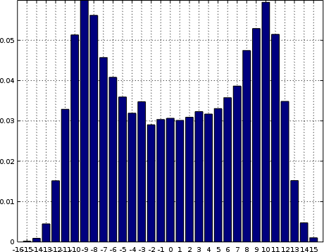
Histograms can also be used to find and diagnose the not-so-normal things that might go wrong. For example, can you guess what’s going wrong in Fig. 9?
 |
In this case, the top bit of the data sample got corrupted by what appears to
be random data, creating the appearance of two nearly identical
Gaussian
shapes. Alternatively, your data might be off cut, and so the samples might
include the LSB from one sample followed by MSB:1 of another.
Off cut data is important to recognize, especially since some particular LVDS protocols can be a challenge to synchronize to the sample boundaries of.
 |
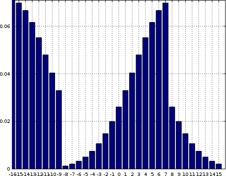
Another possibility is that your LSB might be corrupted. In this case, you’ll see something looking closer to a comb, as shown in Fig. 10 on the right.
As one final example, let me draw your attention to Fig. 11 on the left. In this case, the top two bits of the sample value have been corrupted, but the rest look good. Notice how our Gaussian shape has been split into four jumbled parts?
 |
Remember, no A/D is perfect. You aren’t likely to see shapes this clean in reality, but the general rules above still apply.
The good thing about all of this is that the human brain can detect patterns very easily, and being able to visually see these patterns is the power and reason for calculating and plotting a histogram. Consider how many faults we just diagnosed by examining the patterns above–each was distinct, and each indicated a different form of fault.
So, if a histogram. is so valuable, how shall we measure one?
Calculating a Histogram
Perhaps the easiest way is to record a set of samples and then download them into a program where you can do ad-hoc and scripted data manipulation. I will often use Octave for this purpose, but I am also aware that much of the engineering community likes to use Matlab. (I just can’t afford Matlab, and Octave tends to do everything I need.)
My first rule of digital logic design is that all FPGA logic shall be pipelined so as to be able to process at least one sample per system clock. Throughput is your friend, embrace it!
My second rule is that all signal processing blocks should be controllable across a bus of some type. That means, you should be able to read status from within the system, turn on and off various signaling elements, adjust gains, etc. all from a CPU connected to your design. This CPU can be within your FPGA, such as the ZipCPU that lies within many of my own designs, or it can be external to your design, communicating to your design via some form of debugging bus.
In the first DSP design I built, I used a recursive averager to measure the histogram of an incoming signal.
 |
I would write to my bus peripheral the sample value I wanted to measure the probability of, and also a averaging coefficient. Then, on every sample, if the sample matched the chosen address I would average a one else a zero. Using the recursive averager we studied earlier, this might look like,
	iiravg #(.LGALPHA(5), .IW(1), .OW(BUS_WIDTH))
	iir(i_clk, i_reset, i_ce,
		(i_sample == chosen_sample) ? 1:0, hist_output);
The bus
peripheral the
could then set chosen_sample and read the hist_output result.
	always @(posedge i_clk)
	if (i_wb_stb && i_wb_we)
		chosen_sample <= i_wb_data;

	always @(*)
		o_wb_stall = 1'b0;

	always @(posedge i_clk)
		o_wb_ack <= i_wb_stb;

	always @(posedge i_clk)
		o_wb_data <= hist_output;
This worked great for me in the past when I only wanted to examine one or two bins. The advantage of using this method is that the histogram output is always available to be read. No scaling is needed, the decimal point is right where you want it and you are reading a fractional number. Even better, the logic involved with building this is quite simple, and so it can be done when hardware is at a premium.
The disadvantage with this approach comes when you want to measure more than one bin. In that case, you might walk through the various sample values, wait for the averager to settle and then read the result before moving on. This was my go-to solution until I actually tried it. I then swallowed hard and convinced myself that I liked the result, but I also realized the solution would be completely unworkable with an A/D having 5-bits or more.
Another approach I tried was to run a series of recursive averagers, each focused on a different sample.
 |
The problem with this multi-average approach is simply that the recursive averager approach doesn’t scale well to large numbers of potential sample values.
Another approach is needed, which we’ll discuss building today: the block average approach to generating a histogram. This approach will be centered around using a block RAM element to keep the logic down.
The concept of a block average is really quite simple, and it’s easy to write
out in C. You simply pass to your block processing routine a set of nsamples
samples, captured in a data array, as well as an array to capture the
resulting
histogram.
calculate_histogram(int nsamples, int *data, int *histogram) {The first step is to clear the histogram array.
	for(int k=0; k<(1<<NUM_ADC_BITS); k++)
		histogram[k] = 0;
After that, we’ll walk through all of our sample points, and increment the bin counter in the histogram memory once for every sample in our incoming data.
	for(int k=0; k<nsamples; k++)
		histogram[data[k]]++;
}
That seems easy enough. It’s even easy enough to write out most of the hardware necessary to do this.
 |
Not bad, but can we build it in Verilog?
Well, sort of and … not quite. I mean, the operation is fairly easy to describe in Verilog. Just like the hardware diagram above, it looks easy. The problem is that, just because you can describe it in Verilog doesn’t mean it can properly map to hardware.
always @(posedge i_clk)
if (i_ce)
	mem[i_sample] <= mem[i_sample] + 1;
Indeed, as we’ve written it out, this is language compliant. Even better, it’s likely to work quite well in a simulator. It’s just not likely to map well to all of the different varieties of FPGA hardware.
To capture the problem, I introduced several rules for using block RAM within my beginners tutorial. These rules help to guarantee that your design will successfully map into block RAM rather than flip-flops.
- Rule: When reading from memory, only the read from memory logic shall happen on any given clock. This shall happen within its own always block, with nothing more than a (potential) clock enable line controlling it.
One reason for this rule is that not all FPGA hardware supports reading from block RAM and processing the result on the same clock. Notably the iCE40 series can only read directly into an attached set of flip-flops (the one clock requirement), and from there any value read can only enter into your design logic on the next clock cycle. Even for those FPGAs that can read from a memory directly into an operation, many of them have limited sizes of memory that can support this. While 5-bit A/Ds would work well, wider 10-bit A/Ds could easily overload this capability.
While unfortunate, it is also a reality that if you want to create code that can work efficiently on multiple FPGA architectures then you will need to support the lowest common denominator. That means we’re going to need to split our read out into a separate clock cycle. The result might then look something like,
// Read from memory on the first cycle
always @(posedge i_clk)
	memval <= mem[i_sample];

// Keep track of which sample we are examining,
// and whether or not we'll need to write this
// updated value to memory
always @(posedge i_clk)
	{ r_ce, r_sample } <= { i_ce, i_sample };

// Finally, write to memory on the next cycle
always @(posedge i_clk)
if (r_ce)
	mem[r_sample] <= memval + 1;;
While this gets us closer, there are still two more block RAM rules.
- Rule: When writing to memory, nothing but the memory write shall exist within that logic block. That is, you should only ever write from a register to memory, never from a LUT’s output to memory.
This issue is more timing driven than hardware architecturally driven. Part of the issue here has to deal with the fact that block RAM memories tend only to be located on specific parts of the FPGA. They aren’t necessarily uniformly sprinkled around the fabric. As a result, there may be an unpredictable distance from your logic to the memory, and going from flip-flop to memory helps to mitigate any timing problems there.
This now means that we’ll need to take three clocks to update one value in our histogram estimate. Our first clock will be used to read from memory, our second clock will add one to the result, and our third clock will write the updated result back to memory. Fig. 15 attempts to diagram how this might work.
 |
Again, on its face, this looks like it should be doable. The Verilog to describe this operation remains straightforward.
//
// First clock: read from memory
always @(posedge i_clk)
	// Take a whole clock to read from memory
	memval <= mem[i_sample];

// and keep track of the sample value
always @(posedge i_clk)
	r_sample <= i_sample

// Second clock: add one to the memory value, and
// move r_sample into the next clock cycle as memaddr
always @(posedge i_clk)
if (cepipe[0])
begin
	memnew <= memval + 1;
	memaddr<= r_sample;
end

// Last clock: write the result back
always @(posedge i_clk)
if (cepipe[1])
	// Take a whole clock to write to memory
	mem[memaddr] <= memnew;

//
// Don't forget we'll need to keep track of the
// original i_ce value, and delay it by two cycles
// to get it into the third clock period.
always @(posedge i_clk)
	// Delay i_ce to control our write-to-mem action
	cepipe <= { cepipe[0], i_ce };
That is, it looks doable until you start getting into the details. For
example, what happens if you receive the same sample value for several
clocks in a row? Let’s say we receive sample value 0 for 7 clocks in a row.
 |
After receiving i_sample=0, we read from memory. Let’s suppose we start from
zero for the sake of simplicity. Therefore, memval=0 on the next clock
cycle, memnew=1 on the cycle after that, and mem[0]=1 on the following
cycle. Finally, on the next cycle memval can read the value 1 from memory.
The result is that after receiving our value across seven different clock cycles, we’ve only marked three counts into our bin counter–not seven.
Remember our goal of high throughput? We want to be able to process every sample at a rate as high as our FPGA will allow. That means we want to be able to accumulate one sample per clock across several clocks as we did above.
This is going to be a problem. We’re going to need to solve it in order to build a good generic histogram. That said, we’ll come back to this again when we have the formal tools helping us out. That’ll make it a lot easier to work out.
There’s also the issue of initializing our array that we haven’t yet discussed. This brings us to the last rule for block RAM allocation:
- Rule: You can’t initialize all of a memory at the same time. You can only start the memory with known contents, and then write to one address in memory (or not) on any subsequent clock tick.
This may be more of an FPGA rule than an ASIC rule. The problem is that most FPGA block RAMs have no capability for adjusting every value of the memory at once. You can access one, or sometimes two, values at a time but never clear the whole array.
This particular rule is even more annoying than the last two, and it’s going to take some work to accomplish. The good news, though, is that we’ve now got an open clock between our memory read and our memory write that we can use for … whatever logic we want. This will be where we place our initialization.
// Second clock tick, after reading from memory
// into memavg.
always @(posedge i_clk)
if (initializing)
begin
	// Clear another address of memory
	// as part of our reset cycle
	memaddr <= memaddr + 1;
	memnew  <= 0;
end else begin
	// Add one to the last sample value
	// we've seen from our input
	memaddr <= r_sample;
	memnew  <= memval + 1;
end

// Keep track of which step in our pipeline
// is processing input data, and use it to
// turn on memory writes
always @(posedge i_clk)
if (initializing)
	// Write to memory, ignore incoming
	// data when resetting
	cepipe <= 3'b010;
else
	cepipe <= { cepipe[0], i_ce };

// Finally, if cepipe[1] is ever true, write our
// result (or zero) to our histogram memory
always @(posedge i_clk)
if (cepipe[1])
	mem[memaddr] <= memnew;
Okay, so we’re going to need more than that, but you should be able to get the gist of the idea from just that alone.
A simple and fairly basic state machine can then be used to control our reset. The states will look like: 1) Reset, 2) Initialize memory, 3) Count samples, 4) Switch memories, 5) Initialize the new memory, 6) Count samples into the new memory, and so forth.
 |
By using two separate memory sections, one will always be valid and available to be read. That way, while we are resetting and then accumulating counts to generate a histogram in one memory section, the other section will hold the counts from the last average. In this manner, user code will not need to synchronize to the histogram–it will always be there.
Of course, one disadvantage is that something might happen while we are resetting the histogram memory that would then be missed. Whether that is important to you or not is application dependent. Similarly, how you go about fixing the problem is also application dependent. On some applications, data might arrive slow enough that a FIFO can hold on to it during our reset, but I digress.
For now, let’s turn to examining how we are going to build this.
The Formal Contract
Before diving into the details, let’s just quickly examine at a top level how we might verify a histogram. I like to call this the contract: a formal description of how a design is supposed to work that then forms the framework for laying the details out. In this case, our contract consists of little more than a counter.
First, we’ll pick the address of an arbitrary value in memory.
(* anyconst *) reg [AW:0] f_addr;Or rather, we’ll let the solver pick an arbitrary address–that way we can be
assured that the properties of the memory at the chosen address could easily
be applied to all all memory locations. This is the purpose of the
(* anyconst *) attribute.
Next, we’ll create a counter to describe how many times we’ve seen this value. These will become the counts that we read from our design across the bus later on.
	initial	f_this_counts = 0;
	always @(posedge clk)
	if (start_reset || resetpipe)
	begin
		// Clear our special value on or during any reset
		if (activemem == f_addr[AW])
			f_this_counts <= 0;

	end else if (i_ce && { activemem, i_sample } == f_addr)
		// In all other cases, if we see somthing, accumulate  it
		f_this_counts <= f_this_counts + 1;
Remember, we’ve chosen to use two memories–one where we accumulate values,
and the second which we can later read from using the system bus. The value
activemem above captures which memory we are examining. Hence, if i_ce
is ever true, that is if we have a new sample, and if i_sample matches
the special sample we’re going to examine during our proof, then f_this_counts
should increment.
Now we just have to prove, later on, that this value actually matches the value in memory.
	always @(*)
		assert(f_this_counts == mem[f_addr]);
Only … our three clock addition is going to make this comparison a bit more difficult.
At any rate, that’s our goal–matching that value, but in memory. Let’s see how we can go about getting there.
Building the Histogram Peripheral
It’s now time to build our
peripheral.
Let’s pick some number of counts we wish to average together, and how big
our incoming samples will be (AW bits).
We can then declare the I/O port list for our module.
//
module	histogram #(
	parameter	NAVGS = 65536,
	localparam	ACCW = $clog2(NAVGS+1),
	localparam	DW = 32,
	parameter	AW = 12,
	localparam	MEMSZ = (1<<(AW+1))
	) (
	input	wire	i_clk,
	input	wire	i_reset,
	//
	input	wire	i_wb_cyc, i_wb_stb, i_wb_we,
	input	wire [AW-1:0]	i_wb_addr,
	input	wire [DW-1:0]	i_wb_data,
	input	wire [DW/8-1:0]	i_wb_sel,
	output	reg		o_wb_stall,
	output	reg		o_wb_ack,
	output	reg [DW-1:0]	o_wb_data,
	//
	input	wire		i_ce,
	input	wire [AW-1:0]	i_sample,
	//
	output	reg		o_int
	);
I’m going to try something new this time–building the design for one of two
bus structures, either
Wishbone
or
AXI. To keep
our notation constant across both, we’ll create a new clock value, clk,
and a new reset value, reset. We also want to capture when a bus write is
taking place. We’ll later use that as an out of cycle cue of when to start
accumulating values into our
histogram
bins.
	wire	clk   = i_clk;
	wire	reset = i_reset;
	wire	bus_write = i_wb_cyc && i_wb_we;
Memory really needs to start initialized, so let’s give all of our memory an initial value.
	integer	ik;
	initial	begin
		for(ik=0; ik<MEMSZ; ik=ik+1)
			mem[ik] = 0;
	end
Much to my surprise, this turned out to be an intensive process for SymbiYosys–particularly because the memory is so large (2^10 entries). So, instead, I simplified this process for the formal proof and turned it instead into,
	always @(*)
	if (!f_past_valid)
		assume(mem[f_addr] == 0);
But we’ll have more on that later when we get to our formal verification section.
We’re also going to need to count samples going into our
histogram, so we know
when we’ve accumulated a full (parameterized) NAVGS counts. Here we have
a basic counter that just counts up on any new sample, but never quite reaches
NAVGS.
	initial	count = 0;
	always @(posedge clk)
	if (start_reset || resetpipe)
		count <= 0;
	else if (i_ce)
	begin
		if (count == NAVGS[ACCW-1:0]-1)
			count <= 0;
		else
			count <= count + 1;
	end
Why not? Because when we get to one less than NAVGS, we are going to set
a flag indicating we want to start a reset cycle, start_reset.
	initial	start_reset = 1;
	always @(posedge clk)
	begin
		start_reset <= 0;

		if (i_ce && (count == NAVGS[ACCW-1:0]-1))
			start_reset <= 1;
I mentioned above that I also wanted to be able to command a reset from the bus, so let’s allow a bus write to initiate a reset cycle as well.
		if (bus_write)
			start_reset <= 1;
Two other little details: we don’t want to start a reset cycle if we are already in one, unless we get an actual reset signal.
		if (resetpipe)
			start_reset <= 0;
		if (reset)
			start_reset <= 1;
	end
Getting this to only recycle once, and to make certain that every memory value got cleared on reset, took more work than I was expecting. One part of that work is a signal that we are on the first clock of our reset sequence.
	always @(posedge clk)
		first_reset_clock <= start_reset;
The second part is a flag I call resetpipe. The idea with this signal is that
if ever resetpipe is true, we are then in a reset cycle where we zero out
our memory, otherwise we’ll be in normal operation.
	initial	resetpipe = 0;
	always @(posedge clk)
	if (start_reset || first_reset_clock)
		resetpipe <= 1;
	else if (&memaddr[AW-1:0])
		resetpipe <= 0;
There’s one last part to our reset: once we get to the maximum number of counts, we’ll want to switch memories. Further, on any memory switch, we’ll set a user interrupt–so an attached CPU can know that there’s new histogram data which may be examined.
	initial	activemem = 0;
	initial	o_int = 0;
	always @(posedge clk)
	begin
		o_int <= 0;
		if (i_ce && !start_reset && count == NAVGS[ACCW-1:0] -1)
		begin
			activemem <= !activemem;
			o_int <= 1;
		end

		if (reset)
			o_int <= 0;
	end
Put together, a memory swap and reset re-initialization should look something like the trace shown in Fig. 18 below.
 |
The basic sequence is that, when we get to the end of our count, start_reset
goes high. resetpipeline then goes high on the next count and stays high
while we write zeros across all of our memory. Once we’ve cleared all memory,
we’ll start accumulating into our
histogram
into the just cleared bins again.
Notice that change in activemem, noting that we switched histogram banks.
At the same time we switched banks, we also issued an o_int to indicate
that the new data was now valid in the older bank.
In a moment, we’ll start working our way through the three cycles required
by a bin update. I’m going to use a three bit shift register, cepipe, to
capture when new or valid data works its way through our pipeline in what I
like to call a travelling clock enable
(CE)
approach.
	initial	cepipe = 0;
	always @(posedge clk)
	if (resetpipe)
		cepipe <= 3'b010;
	else
		cepipe <= { cepipe[1:0], i_ce };
That’s all of the necessary preliminary work. Now let’s work our way through those three clock cycles.
On our first clock cycle, we’ll read from memory,
	always @(posedge clk)
		memval <= mem[{ activemem, i_sample }];
and record the address we read from–since we’ll need to know that again later.
	always @(posedge clk)
		r_sample <= { activemem, i_sample };
On the next clock cycle, we’ll want to add one to memval, and then write it
back to memory. Only … it’s not that easy.
To clear this up, let’s allow that we are going to write to memaddr a value
of memnew. While we are in the middle of a reset cycle, we’ll increment this
address across all memory spaces and write zeros into all spaces. The only
exception is on the first clock tick, when first_reset_clock is active. On
that tick, we’ll make sure that we are starting from the beginning of memory.
	initial	memaddr = 0;
	initial	memnew  = 0;
	always @(posedge clk)
	if (resetpipe)
	begin
		memnew  <= 0;
		//
		memaddr <= memaddr + 1;
		if (first_reset_clock)
			memaddr <= 0;
		memaddr[AW] <= activemem;
	end else begin
Now that the reset is out of the way, we’ll want to write a new value to
what was the i_sample bin from the last clock tick, but now the r_sample
bin. From that memory, we read memval and so now we want to update it and
place the update into memnew.
		memaddr <= r_sample;

		// We haven't used this value yet, so it's memory
		// copy is up to date--add one to it
		memnew  <= memval + 1;
Of course, the problem is … what if we just updated this value in the last
cycle? That is, what if we are now writing memnew to memaddr? It’ll take
two clock cycles before we can read it back again! We can avoid this problem
with a simple check that we are writing to memaddr on this cycle, and just
add one to our current accumulator.
		if (cepipe[1] && r_sample == memaddr)
			memnew  <= memnew + 1;
This is sometimes known as operand forwarding–rather than going through a register file, we’re short-circuiting the operation and going straight back into our accumulator.
Only … that’s not enough. If we had written to memory on the last cycle, it would still take us another clock to read that value back. So let’s set up a second stage of operand forwarding as well, to grab the value that was just written to memory—but skipping the memory read.
		else if (cepipe[2] && r_sample == bypass_addr)
			memnew  <= bypass_data + 1;
	end
This is how we’ll go about avoiding the problems shown in Fig. 16 above.
We’re finally on our third clock tick. At this point, we simply write
our memnew value to memory at address memaddr.
	always @(posedge clk)
	if (cepipe[1])
		mem[memaddr] <= memnew;
There’s one last step required: we need to keep track of the last value written to memory, lest we want to bypass the memory and go straight back into our accumulator as described above.
	always @(posedge clk)
	begin
		bypass_data <= memnew;
		bypass_addr <= memaddr;
	end
All that’s left now is to work our way through the Wishbone peripheral logic.
At this point, this is easy. On any clock tick, we read from the
address given by i_wb_addr and the memory bank that we aren’t currently
writing into. That’ll give us clear access to a clean
histogram,
rather than one that’s still updating.
	always @(posedge clk)
	begin
		o_wb_data <= 0;
		o_wb_data[ACCW-1:0] <= mem[{ !activemem, i_wb_addr }];
	end
We’ll also immediately acknowledge any request, and keep our stall line low so we can accept requests at all times.
	always @(posedge clk)
		o_wb_ack <= !reset && i_wb_stb;

	always @(*)
		o_wb_stall = 1'b0;
Adjusting this to handle AXI
For those who want to adjust this core to work with an
AXI4 bus,
this transformation can be done quite easily. First, you’ll want to use either
AXILDOUBLE or
AXIDOUBLE
to simplify out the protocol. Once done, the bus has been simplified for
you. For example, all of the ready signals in the simplified slave may be
assumed to be high, and AWVALID and WVALID are the same signal. This
makes interacting with the AXI4 bus much easier than it was the last time
we tried this.
First, we’d adjust the name of our clock and reset.
	wire	clk   = S_AXI_ACLK;
	wire	reset = !S_AXI_ARESETN;
	wire	bus_write = S_AXI_AWVALID && S_AXI_WSTRB != 0;
We can also assign bus_write based upon S_AXI_AWVALID alone, and use that
to initiate a reset sequence.
Further down in our file, we’ll set our return values. In particular, we’ll
want to return the read data into S_AXI_RDATA.
	always @(posedge clk)
	begin
		S_AXI_RDATA <= 0;
		S_AXI_RDATA[ACCW-1:0] <= mem[{ !activemem,
			S_AXI_ARADDR[$clog2(C_AXI_DATA_WIDTH)-3 +: AW] }];
	end
Finally, we’ll just hold the read and write responses at a constant “OKAY” value.
	always @(*)
		S_AXI_BRESP = 2'b00;

	always @(*)
S_AXI_RRESP = 2'b00;- Note that the AXI4 peripheral code above is only representative. It has not been (yet) been properly formally verified.
I find this easier to work with than the full AXI4 protocol. It gets past all of the problems others have had, although it will only work in the context of using a pre-protocol processor such as AXILDOUBLE for AXI-lite or AXIDOUBLE for pre-processing AXI4.
That’s it! You now have a working AXI4 peripheral, for almost as little work as would be required for building a straight Wishbone peripheral. The protocol pre-processor takes care of all of the back-pressure issues, AXI4 IDs, AXI4 burst transactions, and so forth–making your job building a bus slave much simpler.
Formally Verifying our Histogram
Now that we’ve gotten this far, let’s see what it takes to formally verify this design.
We’ll start with the obligatory f_past_valid register, that then gives us
access to being able to use $past() in an assertion later on.
`ifdef	FORMAL
	// ...

	reg	f_past_valid;
	initial	f_past_valid = 0;
	always @(posedge clk)
		f_past_valid <= 1;
We’ll also use f_mem_data as short-hand for the value in our solver-chosen
memory address.
	always @(*)
		f_mem_data = mem[f_addr];
Since we skipped initializing the whole memory in order to make the proof run faster, let’s just assume that the initial value is zero.
	always @(*)
	if (!f_past_valid)
		assume(mem[f_addr] == 0);
Functionally, this acts the same within a formal environment as
initial mem[f_addr] = 0; would, but I hesitate to modify
the core’s
operational logic in the formal verification section.
Next, since the Wishbone
interface
is so simple, I’m going to take a risk and not include my formal Wishbone
property file. Instead,
I’ll just assume that if i_wb_cyc is low then i_wb_stb must be low as well.
That’ll at least make the traces look closer to what we want, even if it doesn’t
functionally affect anything we are doing above.
	always @(*)
	if (!i_wb_cyc)
		assume(!i_wb_stb);
You’ve seen above how we are going to accumulate bin counts
into f_this_counts. Here’s where that code lies.
	initial	f_this_counts = 0;
	always @(posedge clk)
	if (start_reset || resetpipe)
	begin
		// Clear our special value on or during any reset
		if (activemem == f_addr[AW])
			f_this_counts <= 0;

	end else if (i_ce && { activemem, i_sample } == f_addr)
		// In all other cases, if we see our special value,
		// accumulate  it
		f_this_counts <= f_this_counts + 1;
Further, to keep track of the register forwarding issue, I’m going to create
another value similar to the cepipe register for watching the update of our
special value work its way through our logic. In this case, it’s going to be
for watching any request for our special operand as it transits through the
system. Hence, if f_this_pipe[0], memval should equal the value from our
special address and r_sample should match i_sample. If f_this_pipe[1],
then we’ve just added one to the value from our bin and so forth. The only
special trick is that we want to clear this value during the reset cycles.
	initial	f_this_pipe = 3'b000;
	always @(posedge clk)
	if (resetpipe)
		f_this_pipe <= 3'b000;
	else
		f_this_pipe <= { f_this_pipe[1:0], (!start_reset && i_ce
				&& activemem == f_addr[AW]
				&& i_sample == f_addr[AW-1:0]) };
Now let’s go check our counter. During a reset cycle, the counter should be zero.
	always @(*)
	if (resetpipe && activemem == f_addr[AW])
		assert(f_this_counts == 0);
Otherwise, if we aren’t updating the value, then it should match what’s in our block RAM.
	else if (f_this_pipe == 0)
		assert(f_this_counts == f_mem_data);
Induction will require just a touch more work.
In the case of
induction,
if ever f_this_pipe indicates only a single value,
then it’s the value we just read from memory into memval following seeing
i_sample at the input. It should be identical to what our f_this_counts
value was one clock ago–that is before it just got updated.
	always @(posedge clk)
	if (f_this_pipe == 3'b001)
		assert(memval == $past(f_this_counts));
Now, once we add one to this value, it should equal our counter post update
as well–just one clock later, only it is now kept in memnew.
	always @(posedge clk)
	if (f_this_pipe[1])
		assert(memnew <= $past(f_this_counts));
Finally, if f_this_pipe[2] is ever true, then we’ve just written to memory.
The value in bypass_data should match f_this_counts just after it was
updated–only now we’re two clocks later.
	always @(posedge clk)
	if (f_this_pipe[2])
		assert(bypass_data == $past(f_this_counts,2));
Let’s also check writing to the data. As you may recall, we write to the
memory on the third clock of our pipeline, whenever the cepipe[1] bit of
our shift register is true. On the clock after any such write,
our counts value (two clocks ago) should now match what’s in memory.
	always @(posedge clk)
	if (f_past_valid && $past(f_past_valid) && cepipe[1]
			&& { activemem, memaddr } == f_addr
			&& !resetpipe)
		assert(f_mem_data == $past(f_this_counts,2));
Finally, we also need to check that f_mem_data is properly reset as part of
the reset cycle. Note that the check below checks the memory bank, kept in
f_addr[AW] against the active memory bank separate from the inequality
checking whether or not the current bank has been cleared or not.
	always @(*)
	if (resetpipe && !first_reset_clock
			&& activemem == f_addr[AW]
			&& memaddr[AW-1:0] > f_addr[AW-1:0])
		assert(f_mem_data == 0);
Finally, one other check on f_this_pipe: If ever any of its values are true,
the corresponding cepipe value must be true as well.
	always @(*)
	if (!resetpipe)
		assert((f_this_pipe & cepipe) == f_this_pipe);
If this looks like just a bunch of minutia, its not nearly as bad as it looks.
I started with just some very simple properties, like the two listed below:
that the data in memory could never exceed NAVGS nor could our counter ever
exceed that value.
	always @(*)
		assert(f_mem_data <= NAVGS);

	always @(*)
		assert(f_this_counts <= NAVGS);
This led to the need to also assert that our number of counts needed to be
less than the counter, count.
	always @(*)
	if (!start_reset && !resetpipe && activemem == f_addr[AW])
		assert(f_this_counts <= count);
While these assertions might seem quite straightforward, working through the design so as to pass induction then lead to many of the other assertions I’m presenting here. Then, once the design passed induction at 80 steps, I shortened the length to 10 steps. When the final assertion was in place to verify the design at 10 steps, I was then able to shorten the proof further to 6, where it stands today.
Let’s take a moment to look through the reset sequence next. In particular,
we want to make certain that the count remains at zero throughout the reset
sequence. It will start incrementing again once we start accepting samples
again after the reset sequence is complete.
	always @(*)
	if (resetpipe)
		assert(count == 0);
Similarly, we’ll want to check that we can get into and start a reset properly.
In particular, we want to initiate a reset anytime we accept a value while
the count it just less than NAVGS.
	always @(posedge i_clk)
	if (f_past_valid && $past(!reset && !start_reset && i_ce && !bus_write)
		&& $past(count == NAVGS-1))
	begin
Once we start this sequence, we’ll want to change our memory bank, activemem,
set an interrupt, o_int, reset the count, count == 0, and raise the
start_reset flag.
		assert(o_int);
		assert($changed(activemem));
		assert(start_reset);
		assert(count == 0);
	end
If you look at this another way, we want to assert an outgoing interrupt anytime we switch memory banks (except following a reset) and at no other times.
	always @(posedge i_clk)
	if (f_past_valid && !$past(reset) && $changed(activemem))
		assert(o_int);
	else
		assert(!o_int);
That’s enough to pass induction, but … does the design even work?
Cover Checks
To convince ourselves this design actually works, rather than just passing a set of abstract property checks, we’ll run some cover checks on the design.
In particular, let’s prove that we can actually achieve a data count equal to the number of averages we are doing.
	always @(*)
		cover(f_mem_data == NAVGS);
You can now see in the trace below how this looks.
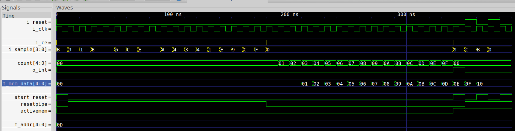 |
The trace starts out with a reset, and then walks through clearing all memory.
We then accept sixteen samples of 4'hd–exactly NAVGS. The design then
switches memory banks and starts the reset on the new memory bank–exactly
like we wanted!
Well, almost. I mean, you could get picky. For example, the design re-enters
the reset state several times at the end because we never kept i_reset from
going high again, but this doesn’t really impact what I wanted to show. If
we had wanted to get fancier, we could’ve added more criteria to the cover()
command.
Conclusion
Calculating a histogram of your incoming data is a very basic analysis task that you will want to be prepared to accomplish as you build any system. There are lots of bugs you can diagnose just by looking over the resulting histogram, as we’ve seen above. Further, if you choose to use a block histogram calculation routine, the logic can be really straightforward.
That said, it wasn’t as simple as you might think. In particular, the three rules of block RAM memory added to the complexity–even though they helped make certain our design fit into a block RAM in a first place. These rules forced us to read from memory in one cycle, calculate an updated value on the next, and finally write the result on the third. Further, since you can’t clear all of a memory at once, you can also see how a basic state machine can make that happen.
Even better, I was able to demonstrate how simple an AXI4 peripheral can be made to be using either the AXILDOUBLE or AXIDOUBLE pre-protocol processors. Indeed, our resulting AXI4 peripheral logic was almost as simple to write as the Wishbone peripheral’s logic was.
Finally, if you are interested in this code, or the SymbiYosys script used to drive SymbiYosys when verifying this core, you can find both in my DSP filters project repository.
Likewise reckon ye also yourselves to be dead indeed unto sin, but alive unto God through Jesus Christ our Lord. (Rom 6:11)