
What is a SwiC?
Central to the motivation behind the development of the ZipCPU is the concept of a System within a Chip (SwiC). As I’m now preparing the ZipCPU for a version 3.0 release, it’s worth revisiting this concept to see what it means and then to compare that with how the ZipCPU has been used in practice.
 |
I have defined a SwiC to be a small soft-core CPU within a chip, but specifically where the CPU is neither the purpose of the chip nor the main application within it. Key to this definition is the requirement that the purpose of the chip is not the CPU nor the application the CPU is supporting, but rather that the CPU is more incidental to the application.
Today, I’d like to examine this concept of a SwiC in light of the many years of ZipCPU application and development, to see how well it (or any other CPU for that matter) lives up to this concept.
The initial motivation for the ZipCPU: GPS
The initial application that motivated the ZipCPU was that of a GPS correlator. A GPS correlator consists of a data feed coming from an Analog to Digital Converter (A/D), possibly entering via a DMA to memory, and correlation outputs–perhaps even going as far as soft-bit outputs. The hardware in this case is is centered on the correlator. The correlator just reads and then correlates the data in memory with the spreading code of a GPS satellite. It requires several logic FFTs and a lot of internal memory, together with whatever glueware is required to connect them all together.
 |
An example of one such correlator is shown in Fig. 2 on the left.
So where does the CPU fit in?
My original plan for the CPU was to have it control which satellite’s ranging code would be loaded into the correlator, together with estimating which Doppler offsets to search.
Determining which satellites to correlate against and which Doppler offsets to check requires a CPU. The CPU takes an estimate of where the system thinks the user is on the ground, together with a coarse estimate of the ephemerides for each of the satellites in the constellation. It then uses this information to determine first which satellites are in view, and then second what Doppler shifts can be expected from each of them. The better the CPU can do this task, the fewer correlations that need to be checked and so the sooner the correlators will lock on to the various satellite signals. Once lock has been achieved, the CPU will continue to look for new satellites that might be in view, and estimate what their Doppler offsets would be given the receiver’s known location.
Sure, this task could be offloaded to an external CPU. But what about the task of loading the coefficients and setting things up given the satellite number and the Doppler estimate?
Handling nuisance tasks like this isn’t a major portion of the design logic, but it is a necessary part. Further, since the CPU exists, it can also be used to coordinate reporting and the control of the DMAs to move data around. It could even be used to take the correlation estimates and turn them into positions, but in my world that was always handled externally by a full featured processor.
This is where I came up with the idea of a SwiC: it’s a small, disadvantaged computer, occupying a minor portion of a chip which is devoted to another task entirely.
As an added benefit to starting the ZipCPU project, the hardware required for a minimal CPU is also going to be minimal and even cheap. In contrast, the hardware required for the correlators wouldn’t be cheap at all–especially since the algorithm I wanted to implement was block RAM limited. Indeed, it may have required a VC707–something I couldn’t afford at the time, which kept the project from getting off the ground. The CPU hardware on the other hand? That would definitely form the cheaper part of the project. Indeed, the ZipCPU even demonstrated its ability to run a small Operating System on a $60 Spartan 6 LX4 (smallest Spartan 6). This made it easier to justify the business end of getting started–but I’m getting ahead of myself.
Properties of a SwiC
A SwiC, therefore, must be a small CPU. It must be small enough that it can be added to a design as an after thought. Ideally, it shouldn’t significantly impact the logic or area requirements of the design, simply because it uses so few resources.
That’s the most basic requirement: it must be small.
Must it be fast? Not necessarily, although faster is usually better.
Must it be low power? Maybe, maybe not. Again, that depends on your requirements.
Like all CPUs, however, a SwiC must be a bus master and it must be able to communicate with the environment around it. It must also be responsive to interrupts that may be generated by the application handler. For example, an interrupt might tell the CPU that one round of correlation processing had completed.
These are then the minimum requirements: 1) a small 2) bus master, that is 3) responsive to interrupts. Further requirements may insist that it be 3) fast and/or 4) low power, but these are more ancillary than core requirements.
 |
After that, however, the requirements of a CPU in general start to dominate the problem space. To see how this is so, let’s start at the top.
-
Instruction memory
A CPU, by definition, processes instructions in a serial manner. Therefore a SwiC, like any CPU, must have access to memory containing instructions. These instructions are generally constant, so one may often assume the instruction stream is kept in a ROM.
Sadly, there are enough exceptions to this rule to keep it from being absolutely true. For example, programs must be loaded, updated, and modified over time. It may also be advantageous to move the instruction memory from an offline storage such as an SD Card into an accessible memory. A ROM therefore is a good approximation, but only an approximation.
-
Data memory
A CPU also needs the ability to store and process data in some kind of RAM. This means the CPU must have access to a read and writable memory somewhere, and not just the ROM containing the instructions.
-
Application peripherals
Finally, the CPU needs to interact with the part of the design it was intended to control. These are application specific peripherals that may exist in some designs and not in others. Optionally, these peripherals may generate interrupts that the CPU is required to process.
This might leave you imagining a small bare bones CPU, such as the one shown in Fig. 3 above.
At least, that’s what you might imagine before you try implementing such a CPU.
Reality starts to look more like Fig. 4 below.
 |
Let’s start with how we might go about implementing the instruction memory. Marrying these requirements to commodity FPGA hardware lends to placing the instruction memory into flash memory. Flash memory tends to be slow, but generally abundant for these purposes. The problem with flash is that you need a way to program it before activating the CPU. My general solution to this problem has been to add a second bus master to any system, something I call a debugging bus. This bus master can then access the flash to program it. As a bonus, the debugging bus master can also reach into and control and/or debug the CPU itself. That’s actually important, since the CPU needs to be kept from accessing the flash memory while it is being programmed.
Flash memory, however, won’t pass for data memory. While it is easy to read from, it is hard to write to. So we’ll still need some data memory. Worse, unlike flash memory where the common 16MB size is typically more than enough, a CPU’s data memory usage can quickly expand beyond the capability of any nearby memory. For example, while the standard C library can greatly simplify working with a CPU, that same standard C library may require a minimum of 16kB of memory, and often something closer to 64kB of memory. Over the course of the ZipCPU’s lifetime, this data memory has been provided by block RAM, SRAM, an external SDRAM, or even an external DDR3 SDRAM–all depending on the development board hosting the design. That leaves us with a minimal system having two bus masters, the debugging bus and the CPU, and a minimum of three items on the bus: the flash, data memory, and any application peripherals.
Adding the application peripherals only makes this worse: we now need a bus interconnect that can handle two bus masters and three or more peripherals. Many applications also require access to memory as well, via some form of automated memory transfer or more. All of these accesses need to be arbitrated. Hence, a CPU must now have a general purpose bus interconnect–something not necessarily obvious from our minimum requirements above.
 |
When implementing the ZipCPU, there has been a small set of peripherals that also keep coming up over and over again. Fig. 5 on the right shows an example setup including many of these common peripherals. The first of these is a console port, by which a user can communicate with the CPU. The second is a set of single bit input or output wires, what I call a GPIO peripheral. The next two important peripherals are one or more timers and an interrupt controller.
That means that our simple CPU from Fig. 3 above has now become a much more complicated design component, even more than Fig. 4 suggested, as shown in Fig. 5.
This also means that any minimum CPU can quickly become much more than the bare minimum CPU we started our outline from.
Examples of the Vision
Now that you know the initial application that motivated the ZipCPU, let’s take a moment and look at some other applications. I’ll start this list off with a set of applications I’ve come across where a SwiC, such as the ZipCPU, might do nicely. Then, in the next section, we’ll discuss the reality of how the ZipCPU has actually been used. Let’s start with the exceptionally simple.
-
PLL controller
Some time ago, a user asked on Xilinx’s forums what the easiest way would to control a PLL with an AXI4 interface. A kind helper replied that the easiest way to control a PLL on chip would be with an AXI4 input driven by a MicroBlaze computer.
Herein lies the problem of the SwiC: A simple SwiC having 20-100 instructions might’ve solved the problem nicely. However, if the SwiC needs access to RAM, flash, and an interconnect, then … it might have been easier just to drive the PLL with a simple state machine instead of a full blown CPU. Still, a small SwiC might’ve solved this problem nicely–even if it was a bit of overkill for the problem.
At this level, the SwiC competes with a state machine, and a good state machine will easily use less area. However, a good SwiC will only need to be written, simulated, and verified once in order to know it might properly drive a PLL. Still, the advantage here goes to the state machine. Once you need to drive many dissimilar peripherals, or alternatively once the interaction becomes sufficiently complex, then a single SwiC might start to make sense again.
What other uses might one find for a SwiC?
-
Power Controller
Digilent sells a small color OLEDrgb PMod, suitable for drawing any small image on it. This OLEDrgb, however, has some very specific timing requirements associated with when the various power rails of the OLEDrgb chip within it need to be turned on. Once the power rails had been turned on properly, the OLEDrgb then needed to be configured via a long string of SPI commands.
In a system with a hardware OLEDrgb controller, a small CPU could easily manage this power sequence, followed by the required initialization sequence before getting out of the way of the rest of the hardware.
Yes, a state machine might have worked as well. However, if you have a state machine to control your PLL, and another one to control your OLEDrgbs power and startup SPI, then the cost of the separate areas for these separate state machines, and the cost of there respective memory areas, will soon start adding up. At some point, the SwiC becomes a cheaper solution–especially if it can be kept small, and kept from dominating the rest of the design.
-
Flash memory startup handler
Many of my flash controller designs begin the interaction with the flash using a small startup script. This script is necessary to first reset the flash into a known mode, and then second to issue sufficient commands to the flash to place it into its highest speed mode–typically QSPI with a high speed clock.
This gets more difficult in an ASIC device where the ASIC needs to be manufactured before the flash device is selected. The more modern protocols allow for the flash to be queried regarding which modes it supports, followed by issuing appropriate commands to place the flash into a chosen high speed mode. This is a complicated enough exchange that it makes the most sense to handle this in software. A small SwiC, therefore, might be useful for this purpose.
Here, though, I would note that this should only be required for non–System on a Chip (SOC) ASIC chips. If you had a processor available to you on the chip already, then a simpler solution would have been to start the processor using flash memory in its default state (slow SPI), and then to read the necessary instructions from the flash to move it into a higher speed state for operation normal operation.
-
Flash memory programmer
Yes, I once thought to use the ZipCPU as a flash memory programmer on an FPGA. The problem here lies in how a flash memory is operated. Basically, a flash memory is divided into sectors and pages. Writing to a flash device means either erasing a sector (64k Bytes), whereby all the bits in the sector are set to one, or programming a page (256 Bytes), whereby one or more bits within that page are cleared. This means that programming the flash requires first 1) reading a whole sector, 2) copying it somewhere, and then 3) determining if the sector needs to be erased as a whole, before 4) one or more pages within it needs to be programmed.
While I normally handle this over a serial port, the serial port can be quite slow for this purpose. Why, for example, should a whole sector’s worth of data be read and then written when one might just as easily write the sector to the CPU’s memory and then have the CPU determine locally if the sector needs to be fully erased, or only partially programmed? What if, even better, the data were compressed when going over the serial port, and a CPU on the other end uncompressed it?
In my case, although I built the ZipCPU software necessary to do this, I never quite got annoyed enough to build the host software that would interact with it in order to finish following through with the experiment. Instead, it’s still waiting for me to come back to it and report on how well it works.
-
In one project involving a robotic SONAR device, something was needed to periodically poll and report on multiple voltage level, temperature, and accelerometer sensor readings and to create a telemetry stream from them. A first cut of this project suggested the ZipCPU could handle this task quite nicely. Indeed, communicating with the originally intended sensor set based upon a Dallas Semiconductor 1–wire protocol would’ve required something as complex as a CPU to handle this coordination and communication.
In the end, I chose not to use the ZipCPU. The sensor readings needed strict time stamps, and a minimum of logic was required to guarantee things would be shut down if the voltage or temperature measurements were ever out of normal limits.
-
Hi-Res FFT test bench
One of my earlier projects was to build a high resolution FFT. The algorithm primarily involved a special pre-processor that would take place before a traditional FFT. The results on paper and in off-line testing, however, were spectacular. One individual wrote me, after testing the hi-res FFT algorithm on a frequency shift keyed signal, at his amazement that the hi-res FFT could then distinguish between which “bit” was being sent.
This project earns its place on this list, however, not because of the FFT, nor because of the pre-processor’s implementation, but rather because of the challenge associated with testing it. My initial tests involved sending a tone into the FFT at a programmable frequency, and then evaluating the sidelobes to see how well the tone was isolated. The problem? The amount of data getting sent back and forth rendered sweeping the tone across all frequencies and examining the data from it an exercise in patience.
This project took place before the ZipCPU. Had I placed a small CPU on board, this task might have become much easier: The CPU might have controlled the tone’s frequency, and then estimated the maximum sidelobe–all taking place within the FPGA–reducing the data requirement over the serial port to something much more reasonable, and speeding up the testing significantly.
This is just a short list of the sorts of ideas that have motivated my interest in SwiCs in general. At least, this describes the vision. What about the reality?
ZipCPU: The Reality
Now that I’ve worked with the ZipCPU over the course of several projects, it’s worth asking: how well has this vision panned out to reality? To answer that, I’d like to look through several projects that have included a ZipCPU, to see how well the vision fits or doesn’t.
-
Doorbell controller
One of my earlier projects was a doorbell controller. This probably fits more into the category of SOC than SwiC, but the story is worth telling anyway.
 |
The background behind this project was a 2AM visitor that … well, I have no idea who it was, or why they knocked on our door at 2AM. (By the time I got to the door with my security officer, they were no longer there.) But this got me thinking: it would’ve been nice to turn on the outdoor lights when this person rang the doorbell, and to make sure the lights were otherwise turned off automatically at night.
My thought was to use a small FPGA to control the doorbell and outdoor light together. The outdoor light would be turned on initially at dusk, but eventually turned off–unless the doorbell rang. If anyone rang the doorbell, the outdoor light would turn on for a period of time. That meant that the FPGA would need to know time of day–requiring user interaction to set, hence there was a small keypad and a 2–line LED display.
In this project, the ZipCPU controlled the light, the keypad, the 2–line display, and the audio doorbell.
Wouldn’t a small microcontroller have been more appropriate? Perhaps a Raspberry Pi or even an Arduino? Absolutely.
However, my true purpose was to see how small a system containing the ZipCPU could be, and whether or not the ZipCPU could handle multi-tasking. The answer was, yes it could handle multi-tasking while still fitting on Xilinx’s smallest Spartan 6: the LX4.
(This project was internally funded …)
-
In another project, the customer wanted to generate a special communications signal on an I/O pin. Part of the project involved deciding what signaling standard to use, so several were tried to include two different types of on-off keying and two types of pulse position modulation.
In this case, the application used only a small amount of logic within the FPGA to generate these signals.
A more substantial problem was how to record the results from a test like this. In this case, the ideal recorder was the FPGA: it had access to the incoming signals, a large DDR3 SDRAM attached, as well as an SD Card to make recordings with. While an SD card can become an ideal medium for recording data, the challenge is how to deal with the file system present on the card.
Enter the ZipCPU, the SDSPI Controller, and the FATFS library.
The next challenge was how to deliver the ZipCPU’s program to the customer, who didn’t have the debugging bus infrastructure available to him on his host computer in order to load the ZipCPU. The particular board we had chosen for this project, however, permitted loading the FPGA from an SD Card. Therefore, we chose to load the board from this SD card, and I placed a boot loader for the ZipCPU into 64kB of ROM. (The program required 168 bytes more than the 32kB, forcing a 64kB ROM built out of block RAM.) The boot loader would then walk through a small script to start up the SD Card, and then read a file from it into memory, before jumping to the first address of memory.
Once loaded, the user could interact with the design via a CPU provided menu, allowing the user to configure the test, capture data, and save any data captured to a file on the SD card.
-
Broadband High-Frequency Active SONAR
A more recent project involved the development of a controller for a SONAR transmitter. As with the last project, the amount of logic involved in the transmitter turned out to be a small portion of the project. Still, small or not, it did need to be configured. A small ZipCPU program attached to the serial port provided the customer with a way to control the transmitter, to both turn it on and off, as well as to control the waveform produced by the transmitter: frequency, pulse duration, pulse repetition rate, chirp, pseudorandom noise pattern, etc.
-
Video
When first learning about HDMI video, I struggled to get the timing right to lock onto the HDMI clock using the IDELAYE2 function on my FPGA. (In hindsight, I didn’t understand how the IDELAYE2 element worked, and could’ve greatly simplified this problem …) While I couldn’t lock automatically, I could tell if things were locked. My solution was to use the ZipCPU to measure whether or not the received HDMI signal quality was good enough, and then to adjust the subsample delay timing until it was.
Also, in the same project, I had to deal with the challenge of the EDID display data. The project involved a pass through HDMI signal. Therefore, the downstream EDID information needed to be read and forwarded upstream. There was an opportunity for software to adjust things in the middle. In the end, however, the ZipCPU just copied the EDID information from the downstream monitor to the upstream RPi source and everything worked.
-
One potential customer has asked me about the feasability of overlaying graphical information, such as text and/or menus, onto a video stream. The FPGA would sample data from a camera, apply some special processing algorithms to clean up the image, and then forward the results down stream. It just needed an ability for user control and feedback somewhere. Here, again, the majority of the processing will take place within the FPGA logic. Indeed, it might be possible to do all of the processing in the FPGA logic without a CPU at all. The problem was … the technology was still in development. While in development, it makes sense to be able to reconfigure things. Therefore, the CPU is present to be able to read histogram data, operate on it, adjust scaling constants, and in general to rearrange the configuration as necessary.
In this last case, the CPU may evolve into a more necessary function as well. Because the project is designed to be a “bump” in the video stream, i.e. HDMI and power in, maybe a couple buttons, and then HDMI out, any user feedback regarding the algorithm or its performance will need to be placed onto the video output stream itself. This can easily be done with a text overlay, however a CPU will be required to determine what text to overlay and where. Perhaps I’ll even port the nCurses library to the ZipCPU and integrate that. We’ll see, however, as this project develops–assuming it gets funded in the first place.
-
ASIC testing
There’s another place where a small soft-core CPU can have a big impact, and that’s in simulation testing. When building and testing an ASIC peripheral recently, it helped to be able to simulate the peripheral’s interactions with a nearby soft-core CPU. This, of course, requires having a Verilog CPU nearby which can stimulate the peripheral.
Being an open source CPU, or perhaps more because the ZipCPU was internally sourced, the ZipCPU fit this role quite nicely.
The proposal ended up being a challenge on two fronts, however. The first was speed. A Verilog test script will always beat a Verilog CPU in processing speed. The second was in maintainability. At some point, I needed to hand the software to someone else to maintain, and they weren’t necessarily comfortable with the risk of needing to maintain the ZipCPU’s tool base. Doh!
As you can see from the above examples, the amount of CPU interaction with the design has ranged from something that might be replaced by a small AXI4-lite state machine, to something rivaling an SOC in its own right.
Logic Usage
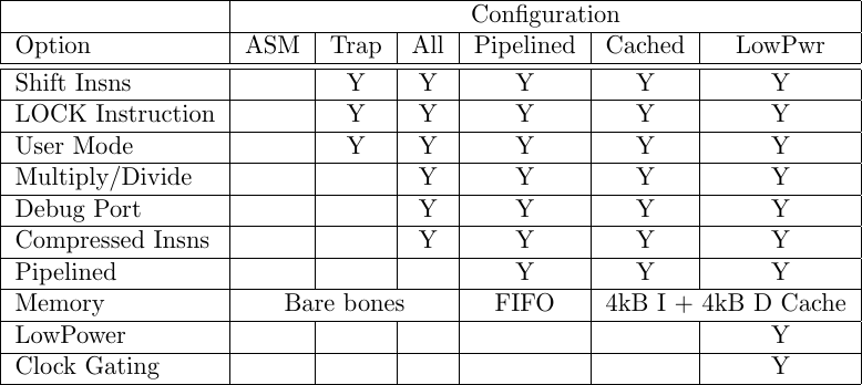
How about logic usage? Let’s take a quick look at logic usage. Does the ZipCPU truly qualify as small enough to be used in a SwiC? This question isn’t so easy to answer, since CPU design always involves a trade off between performance and area. Specifically, you can buy more, better, faster performance with more on-chip area. That means to compare logic usage, we’ll need to define a feature set to measure logic usage from. So let’s define and then compare a couple of configurations:
 |
-
ASM: If you strip the ZipCPU of every single optional feature, you get to this ASM mode. I call it the “ASM” mode because it doesn’t include instructions that the toolchain would require–such as multiplies, divides, or shifts of more than one bit. Worse, because this mode doesn’t include the user mode, there’s no way to trap on an unimplemented instruction–the ZipCPU would either just halt or restart–depending on its configuration. This means that any ZipCPU program using this mode will likely need to be written in assembly.
-
TRAP: This is a compromise from the ASM support above. In this mode, shift instructions are now implemented, and there’s now a user mode that can be used to trap unimplemented multiply or divide instructions. Further, the LOCK instruction is now implemented, allowing atomic access from user mode.
For those buses that don’t support the LOCK instruction, such as the AXI-lite bus, the LOCK instruction instead implements a interrupt block–preventing the ZipCPU from responding to an interrupt for three instructions. Sadly, this includes all of the Wishbone wrappers prior to the pipelined controller, since the LOCK instruction would otherwise cause a dead lock: the data bus would hold the Wishbone cycle line high during the lock operation, and so otherwise it would lock out the instruction bus interface from fetching the next instruction.
-
Minimum: This configuration includes support for all CPU instructions. In particular, it also supports the compressed instruction set not supported by the TRAP configuration above. This isn’t quite a full featured configuration, however, since the ZipCPU isn’t (yet) pipelined. (That’s the next configuration.) Instructions, therefore, take a minimum of four cycles to complete.
The savings between this mode and the pipelined mode (next) is primarily captured by the difference between the memory controllers, shared registers, and some simplified pipeline signaling.
-
Pipelined: The ZipCPU was originally designed to be a pipelined CPU. This configuration turns pipelining on, while also including a powerful memory controller that’s not (yet) quite as capable as a cache.
-
Cached: This configuration adds a 4kB instruction and a 4kB data cache to the CPU’s configuration.
In general, cache sizes are configurable–but this configuration arbitrarily uses 4kB caches.
-
Low Power: This final configuration adds both clock gating (unusable on most FPGAs, but we’ll ignore that for now), as well as zeroing unused registers for the purpose of lowering the CPU’s power requirements.
Just for review, you can see these configurations compared in Fig. 8 below.
 |
That covers the configurations of the core of the CPU.
This isn’t sufficient, however, to measure the CPU’s logic usage, since the CPU needs to be married to a wrapper containing the bus interface and memory controllers. Since the new ZipCPU distribution supports Wishbone and AXI-lite and AXI4, there are three basic wrappers: the ZipBones, Zip-AXIL, and ZipAXI wrappers. A fourth wrapper, one I call the ZipSystem, connects the ZipCPU to an immediate set of local peripherals: one or two interrupt controllers, three timers, a jiffies peripheral, some performance counters, and a Wishbone DMA. Each of these wrappers has a different logic requirement when attached to the ZipCPU core. So examine them one at a time.
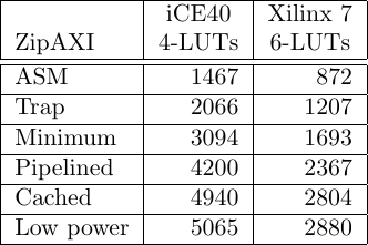
For accounting purposes, I’ll measure CPU usage in terms of both 4-LUTs on an iCE40, and Xilinx 6-LUTs. I will use Yosys for the measurements, and this script to make them automatically.
Let’s start with the ZipBones area usage, as shown in Fig. 9 on the left.
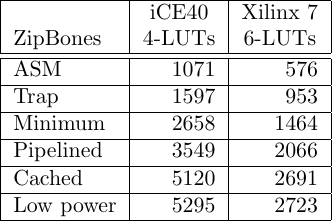 |
As you can see from this table, the ZipBones configuration fits nicely in the smallest of areas. Indeed, I was quite pleased with myself that the CPU can be made to fit in as few as 576 6-LUTs. No, it’s not very usable in that configuration, but that’s about as good as I can get for low-area bragging rights.
The next wrapper we’re examining is the ZipSystem. As mentioned above, the ZipSystem is not a bare CPU, but rather includes includes several local peripherals: three timers, a Wishbone DMA, interrupt controllers, and more. As one might expect, there’s a logic cost to these new features, and this cost can be seen in the ZipSystem’s logic usage chart shown in Fig. 10 on the right.
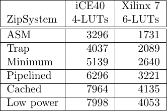 |
In general, the cost of these extra peripherals runs about 1150 6-LUTs or so.
The chart for the ZipCPU’s AXI-Lite wrapper’s logic usage is just a little different. Specifically, I have yet to build any AXI-_lite_ cache implementations. (I have an AXI cache implemention …) Therefore, the usage chart for AXI-lite shown in Fig. 11 doesn’t have any cache options to it.
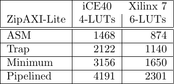 |
For reference, all of these AXI-Lite configurations, prior to the pipelined one, make use of the AXI-lite memory controller we discussed some time ago. As you might guess, there’s no bus support for the LOCK instruction in this configuration since AXI-Lite has no support for exclusive access.
That brings us to the ZipCPU’s final wrapper, showing the AXI4 (full) interface logic usage in Fig. 12 on the right.
 |
This includes the bare minimum AXI4 memory controller we discussed for the minimum modes as well. Since making this measurement, however, I’ve added an exclusive access option to my AXI data cache implementation. So, the numbers may not quite match the current performance.
Having this kind of information, though, is really cool. That means that I can now compare logic usage requirements between the various bus implementations, as shown in Fig. 13 on the left.
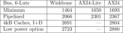 |
One of my contentions has always been that AXI4 is unnecessarily complicated. Here, you can see that, in spite of the extra complications of working with the AXI4 bus, the CPU 6–LUT logic usage difference is only 100-200 LUTs between the Wishbone and AXI4 implementations. On an FPGA with 200k LUTs, this difference isn’t a big deal. On an FPGA with 1,500 LUTs? A 200 LUT difference could mean the difference between fitting and not.
While informative, this bus comparison really isn’t complete. To be complete, the comparison should also the cost of the interconnect and all of the peripherals–each of which would magnify the differences shown here.
When comparing logic usage options, one of the things not shown in these charts is the cost of a Finite State Machine bus controller such as one might use instead of a CPU for relatively simple tasks. For reference, therefore, a simple AXI-lite FSM–based bus controller, reading from a (not-included) memory script, can be made as simple as 88~LUTs.
Comparison to SOCs
So, how does a ZipCPU compare against a full blown SOC? Something like a Zynq, for example?
-
Hardware support. The Zynq is bigger (i.e. more capable), and supports more hardware out of the box. It has hard macros for such things as DDR3 memory, SD Cards, ethernet, displays, and more. Further, because the ARM CPU within the Zynq is implemented out of raw gates, rather than FPGA fabric, it runs at a much higher clock speed.
A SwiC isn’t going to compete well here.
On the other hand, the ZipCPU’s memory controller tends to compare favorably to the ARM when measuring the raw bus access speed of the CPU accessing FPGA logic. I can’t explain this, but I have seen it multiple times over.
-
Logic Portability. One problem with the Zynq, or any other SOC for that matter, is that its peripherals are unique to it. Some may have a device independent interface, similar to
printf()for the ability to interact with a console, but getting to that interface takes a lot of work and capability away from a raw CPU. The ZipCPU, on the other hand, is a soft core CPU. It can therefore (theoretically) run on any hardware, and its peripherals can be ported from one piece of hardware to another for a similar user experience across multiple vendors’ FPGAs. -
Bare-Bones Programming. The ZipCPU runs quite well without any operating system. As we’ve discussed earlier, it’s pretty easy to run multiple threads on the ZipCPU–even without an operating system.
How does this compare the the ARM within a Zynq? Frankly, I haven’t written any bare bones software for the ARM to really know. I know plenty of others have, so I know it’s quite doable. I’d personally be tempted to give the ZipCPU the advantage here, simply because of the ZipCPU’s approach to interrupt handling, but my own subjective view of this matter is hardly definitive and quite likely biased.
-
Simulation. What the Zynq cannot do, however, the ZipCPU can: simulation. Since the ZipCPU is an all Verilog CPU based upon publicly available Verilog, it can easily be verilated into C++, integrated into the host O/S of the simulator, and therefore offer more realistic cycle by cycle simulation of a system under test. If simulation is what you want, therefore, the ZipCPU (or any other soft-core for that matter) easily wins here.
-
ASIC. If I ever need to build a CPU into an ASIC, the ZipCPU will be my go to solution. It’s proven, verified, fits into a small (and controllable) area, and costs less than an ARM.
(I might be a touch biased in this opinion. Use your own discretion.)
Conclusions
Having now reviewed the concept of a SwiC, and seen how such a device might be used, what conclusions might we draw?
-
For a single need, an FSM may make more sense
Even at it’s lowest logic usage of 576 Xilinx 6–LUTs (plus the flash controller, data memory, and interconnect which we didn’t count), the ZipCPU cannot compete with an 88 6-LUT FSM based bus controller.
Sorry, that’s just not going to happen.
-
For multiple needs, an interconnect and console become indispensable. The measure of the CPU’s impact on the rest of the system really needs to include these components.
Simply put, the more things the CPU needs to control, the more things it needs to be connected to.
Why the console? Simple: it’s really easy to use, and even easier to debug with. Debug by printf() is just so much easier than debug by debugger, or even debug via VCD trace, that I’d use it in a heartbeat any time I can.
Unfortunately, the interconnect and DDR3 SDRAM controller by themselves can easily be so costly as to void the whole SwiC vision. Why use a SwiC at all, then? Why not a regular soft core?
-
Even in the presence of big SOC+FPGA devices, small soft-core CPUs can still have a big impact.
While the impact might be reserved to simulation and testing, or vendor independence only, impacts are still impacts.
-
In most of my actual, real-life use cases, the ZipCPU hasn’t really fulfilled my original vision of a SwiC. Instead, it seems to grow and expand to fill whatever space is left on my device.
On the other hand, perhaps that was the vision–especially since I have yet to come across a project where the ZipCPU won’t fit.
The one thing I haven’t tried, though, is connecting the ZipCPU’s fetch directly to a small attached block RAM implemented as an instruction ROM. Doing so would probably both speed up the ZipCPU and lower its memory usage. Let me add this one to my to-do list as well. It won’t be the first item on my list, though–that’s still finalizing the ZipCPU for it’s version 3.0 release.
Expect to hear more of this in the future.
 |
Of course, the sad part of this to-do list, like any good to-do list, is that it just keeps on growing.
Were there is no vision, the people perish: but he that keepeth the law, happy is he. (Prov 29:18)