
Clock Gating
Most libraries contain a clock gating circuit within them. These tend to be designed by an analog hardware designer, rather than the digital designer, for the simple reason that getting the layout right can be critical. Such clock gating circuits are often used as a means of power savings.
The circuit itself tends to be fairly simple. It consists of a clock input, an enable input, a latch, an AND gate, and the resulting output clock.
module clkgate( input wire i_clk, i_en,
		output wire o_clk);

	reg	latch;

	always @(*)
	if (!i_clk)
		latch = i_en;

	assign	o_clk = (latch)&&(i_clk);
Indeed, the circuit is simple enough that I like to assign it to students as an exercise in formal verification.
It’s important this be done right for several reasons. First, clock glitches are bad. They can cause some of your circuit to experience a clock, while other parts do not, while even other parts of the circuit are left in an indeterminate state. Therefore, it’s important to make certain the output clock won’t glitch when the enable line changes–whenever it changes. Second, it’s important that the resulting clock can be used in the same clock domain as the original clock.
Clock gating can be a very important part of ASIC design for power reasons. First, it takes energy to toggle a wire–any wire–within a design. The more often you toggle it, the more power your design then uses. Hence, if you want to lower the power required by a design, then it becomes important to keep as much of the logic within the design from toggling as possible. Second, the greater the capacitance of the wire, the greater the energy that’s required to toggle it. This is especially true of a clock tree, where the clock signal may need to travel through a chip-sized clock tree to get to a large majority of the flip flops within the chip. If, at any point in that tree, the clock can be stopped then both the clock and everything depending upon it can be kept from consuming any further dynamic power.
This makes clock gating an important topic.
FPGAs tend to be both unique and somewhat disadvantaged in this discussion.
Like ASICs,
FPGA libraries also include
clock gates. On Xilinx Series 7
devices, for example, these are BUFGCE library elements that can be used to
gate clocks.
That’s not the what makes FPGAs unique. The difference with FPGAs is that,
unlike ASICs, FPGAs come
with pre-configured clock
trees that tend to
be global (chip-wide) in scale and scope. This fixes their capacitance,
forcing clocks to require a significant amount of energy to toggle in order to
reach the entire clock
tree.
That also means that, in order to gate a clock, you’ll need to create a second
clock from the first one–one that can be gated, and you’ll then need
to place it into a global clock buffer as well. This second clock will only
add to your power usage–unlike an
ASIC where the
clock tree might be
trimmed down so that it is only as big as it needs to be. In other words,
there’s nothing to be gained by gating a
clock within an FPGA other than
perhaps testing and verifying an
ASIC system that might
require clock gating.
Low power in an FPGA system is often achieved therefore, not by a
clock gate,
but rather by a logic signal that can be issued to all flip-flops within a
given design region. We might call this a “Clock Enable”, or i_ce as I tend
to call it. When i_ce is low, nothing transitions and energy is minimized.
This FPGA clock enable power reduction mechanism lends to flip-flop structures that look like:
	always @(posedge i_clk)
	if (i_ce)
		Q <= D;
As long as i_ce stays low, the flip-flop uses a minimum amount of power.
Today, though, I’d like to share some of my experiences with using a clock gating circuit in simulations–independent of the ultimate hardware the design would drive.
Clock Gating in Simulation
When I first tried clock gating in simulation, my purpose was just to learn about clock gating. Is it easy or hard? Eventually, I’d like to be able to add a clock gating capability to the ZipCPU, so that the ZipCPU could be used in an application requiring low power.
I also started this task with a hypothesis:
Hypothesis: Simulation time is proportional to the amount of signals that have to be evaluated each cycle.
For this reason, if the number of signals needing to be evaluated can be greatly reduced due to the presence of a clock gate, then it only makes sense that gating any unused clocks within a simulation will only speed up the simulation. At least, this was my hypothesis starting out.
Gating the ZipCPU’s clock
I decided to build my initial attempts at stopping the
clock
around the ZipCPU’s sleep
functionality. Basically, the ZipCPU
has a WAIT instruction
that puts the ZipCPU to sleep until the
next interrupt. This
seemed like the perfect time to stop the
ZipCPU’s clock. Indeed, the
WAIT instruction
was integrated into the ZipCPU’s
instruction set
for just this purpose.
Then, after thinking about it some more, I started wondering about what the ZipCPU should do if the debugging interface halted the CPU externally? Certainly, if the CPU isn’t enabled, it should stop it’s clock as well, no?
So I built some clock gating logic into the ZipCPU to see what might happen. Once the ZipCPU passed it’s formal checks again, I placed it into a large integrated simulation to test it.
Can anyone guess what happened?
Nothing.
The ZipCPU never came out of reset.
The problem is that the ZipCPU required a clock to acknowledge the reset, and I was starting the design with the clock off.
Oops.
First lesson learned: be very careful how you handle clock enables and the reset signal.
The second problem was similarly ugly: if the clock is off, and the clock gate control logic is controlled by the clock that is off, then you’ll never be able to wake up.
So, after a lot of work, here’s the logic I came up with: It’s split into two parts. Part one is the combinatorial part. This is used to tell us when to wake up. Well, that’s not quite true. Very few things in any digital design are truly combinatorial. Perhaps a better way to say it is that part one consists of logic that will be clocked with the always–on clock, and used to turn the gated clock on and off. Part two is the registered part, registered on the gated clock that is. This is the part I use to help tame the combinatorial logic portion.
Let’s start with the combinatorial part. This part sets an output from the CPU,
o_clken, which is then used to control the clock gate circuit externally.
It’s primarily based upon the registered value, r_clken, but with a few
exceptions.
	assign	o_clken = r_clken || i_dbg_we || i_clear_cache
			|| (!i_halt && (i_interrupt || !sleep));
Basically, we want to wake up on an interrupt and we want to make sure the clock stays running unless we are asleep.
assign o_clken = /* ... */ || (i_interrupt || !sleep);Well, there’s an exception to that rule. If the CPU is commanded to halt
from the debugging interface, then it doesn’t matter if an
interrupt is pending
or if the CPU wants to be awake: the debug interface should always be able to
put the CPU into a deep sleep–that’s the purpose of the i_halt signal.
assign o_clken = /* ... */ || (!i_halt && (i_interrupt || !sleep));What about a debugging
command, such as
writing to a register via the debugging interface, done here by setting
i_dbg_we, or informing the CPU (while it is halted) that external memory
may have changed so the CPU can know to clear its cache? That’s the purpose
of the i_clear_cache signal. In both cases, the
debugger
needs to be able to be able to interact with the design while it’s
asleep. For this we’ll need two additional exceptions.
assign o_clken = r_clken || i_dbg_we || i_clear_cache /* ... */;Everything else can be stuffed into the registered signal, r_clken–part two
of our enable logic.
Let’s take a look at that register, shall we?
The tricky part with this register is the reset. On a reset, the CPU should
only disable the clock if the i_halt input is requesting that we stop.
This would be the case where the CPU is configured to start up into a halted
configuration, or equivalently if the
debugger
has control of the processor and issues it a reset. In this case, a CPU
reset isn’t the same as a
bus reset.
In order to keep from freezing up external buses when rebooting the CPU from
an external input in this fashion, it’s important we keep the clock enabled
until all bus operations are finished. (Remember, resetting an AXI bus
component typically requires resetting the entire
bus and everything
connected to it.)
	always @(posedge i_clk)
	if (i_reset || (i_halt && r_halted && !i_dbg_we))
		r_clken <= i_mem_busy || !i_halt;
The second criteria here has to deal with the debugging
interface. Basically,
if the debugging
interface
raises the i_halt signal, then the CPU is supposed to come to a halt. Indeed,
the CPU will halt once it both finishes its current operation and once the
pipeline is filled again. However, that leads to a lot of times when we can
and cannot halt. For example, the CPU can’t halt in the middle of an
atomic operation that might
lock the bus, lest the rest of the design lock up. Similarly, the
ZipCPU can’t halt in the middle of a
two part compressed
instruction,
nor can it halt while a divide,
multiply,
or memory operation
is pending. That’s why the
ZipCPU
has an r_halted signal–to help tame all these conditions to something that
can be registered. Therefore, if the CPU is halted, and the
debug interface
wants it to stay halted, then we halt and ignore any other criteria. The
exception to this rule is if we want to read from a register using the
debugging interface.
In that case, we’ll need to wake up for a few clocks to read the register.
That’s the first set of criteria, shown above.
The next step controls when we should wake up. In general, we’ll want to
be awake if we aren’t sleeping. We also want to wake up on an incoming
interrupt. The exception
to this rule is that we don’t care about whether or not the CPU is sleeping or
an interrupt is pending
if we’ve been commanded to halt–just like the combinatorial logic driving
o_clken above.
	else if (!i_halt&& (!sleep || i_interrupt || pending_interrupt))
		r_clken <= 1'b1;
Here, again, the
ZipCPU logic attempts to tame
interrupt
handling with two signals: a combinatorial
input, i_interrupt, and a registered signal, pending_interrupt, to deal
with cases where we couldn’t immediately respond to an
interrupt yet still
need to.
In all other cases, we’ll want to halt.
	else begin
		r_clken <= 1'b0;
Well, not quite. There are some exceptions to that rule. (This seems to be the story of a CPU in general–simple logic turns into a lot of exceptions.) For example, if we’ve locked the bus or if we are in the middle of an exclusive access operation, then we don’t want to shut the clock off.
		if (o_bus_lock)
			r_clken <= 1'b1;
Similarly, if we are in the middle of a two-part instruction, then we want to complete the instruction before halting as well.
		if (alu_phase)
			r_clken <= 1'b1;
As you may recall, the
ZipCPU
has a set of compressed instructions. These instructions will pack two
16-bit instructions into a single 32-bit word. While this in itself isn’t
all that unique among CPU’s, the
ZipCPU’s implementation is a bit
unusual. Specifically, the
ZipCPU’s
prefetch
will only ever issue 32-bit instructions at a time, leaving the
CPU with no (current) capability to restart one of these instructions in the
middle. For this reason, the ZipCPU
cannot halt in the middle of a pair of 16-bit instructions. In this case,
alu_phase will be true following the first instruction in any
instruction pair.
By only gating the clock if alu_phase is false, we help to guarantee that
these instruction pairs will always proceed to completion.
Our next condition is that, if the CPU is still busy with some operation–any operation, then we’ll want to keep the clock on until we’ve finished it. This includes memory, ALU divide, the (not-yet-implemented) floating point unit, writing a value to the register file, etc.
			if (i_mem_busy || alu_busy || div_busy || fpu_busy
					|| wr_reg_ce || i_dbg_we
					|| i_bus_err)
				r_clken <= 1'b1;

			if (i_halt && !r_halted)
				r_clken <= 1'b1;
		end
But, in general, that’s the logic required to halt the ZipCPU’s clock. The actual clock halting logic, however, is external to the CPU–so that it can be tailored to the environment containing the CPU. Currently, the clock gating logic is only implemented in the ZipCPU’s AXI wrapper–but that may change in time if clock gating proves to be valuable or useful.
Gating an AXI DMA
What about an AXI component? For example, I’ve built an AXI DMA and it only gets fired up every now and then. Can we gate it’s clock?
Sure, why not?
The big difference between the approach I used for my AXI DMA and the approach I used for the ZipCPU above is that I placed the DMA’s clock gate within the DMA logic itself rather than in an encapsulating wrapper. This gave me access to both the gated clock, the original/raw AXI clock, and the current clock gating signal. This turned out to be quite useful, since I could then keep the skidbuffers on the AXI clock, and the rest of the logic on the gated clock–but more on that in a moment. The unfortunate part of this choice is that it also means that this gating circuit isn’t (currently) portable across devices–but today’s focus is really on simulation only, since I’m really still experimenting with the whole concept in the first place.
Gating the DMA’s clock internally had the nice benefit that I could use flip-flops to latch all of the critical clock gating signals within the design. Further, as mentioned above, I could also run the skidbuffers on the raw AXI clock, and only read them using the gated AXI clock. That meant that the DMA didn’t have to wake up from any kind of sleep until the clock after an incoming bus request.
Speaking of latches, the second big difference in this design had to deal with the logic for the clock gate itself. Instead of a latch, I used a negative edge flip-flop–as I’ll share in a moment. The approach isn’t text book, so I’m not convinced if I like it or not, but it’s pretty simple to build and it passes a formal test nicely.
This new/updated clock gating circuit comes in two halves.
The first half sets a register that we’ll use to control the clock gate.
As before, we’ll use a registered signal, clk_active, to handle most of
our control logic–with the exception that we want to turn the clock on given
any AXI-lite control request on our slave
port.
The first half takes place on the positive edge of the clock. In this
case, we will turn the clock on in response to either an incoming bus request
or, alternatively, if a registered clk_active signal is high. We’ll
come back to clk_active in a moment.
Here’s the portion of the gating circuit that takes place on the positive edge of the clock.
		reg	gatep, gaten, clk_active, r_gate;

		always @(posedge S_AXI_ACLK)
		if (!S_AXI_ARESETN)
			gatep <= 1'b1;
		else
			gatep <= clk_active || awskd_valid
				|| wskd_valid || arskd_valid;
The second half of this circuit moves this gatep value to the negative
edge of the clock. Note that there’s no additional logic on this path, save
for a simple reset check. That’s important since this logic must take place
in a half clock period, rather than a whole clock period.
		always @(negedge S_AXI_ACLK)
		if (!S_AXI_ARESETN)
			gaten <= 1'b1;
		else
			gaten <= gatep;
Once accomplished, we can then create a gated clock much like we did with the latch above.
assign gated_clk = S_AXI_ACLK && gaten;The trick here, however, is that the non-gated logic still needs to know
if the clock has been gated. At issue specifically are the
skidbuffers. These
need to be able to handle any incoming signal no matter whether the clock
is on or off. For this reason, the
skidbuffers
operate on the AXI clock, and not the gated clock. To handle the transition,
I created another signal, clk_gate below, to indicate if the logic on the
gated clock is active on this clock cycle.
While I might set this based upon gaten above, that would involve a second
edge to edge crossing, and indeed one that’s not required. I can
instead just move the gatep signal to the next clock to know whether or not
the clock is active on a given cycle.
		always @(posedge S_AXI_ACLK)
		if (!S_AXI_ARESETN)
			r_gate <= 1'b1;
		else
			r_gate <= gatep;

		assign	clk_gate = r_gate;
The resulting signal, clk_gate, should pass a timing check easier–assuming
this piece of logic ever hits something more than the simulator. (It may not.)
Even better, I can easily adjust my Easy AXI-Lite
design
to integrate this clk_gate signal into the
skidbuffers
control signals:
	assign	axil_write_ready = clk_gate && awskd_valid && wskd_valid
			&& (!S_AXIL_BVALID || S_AXIL_BREADY);

	// And sometime later ...

	assign	axil_read_ready = clk_gate && arskd_valid
			&& (!S_AXIL_RVALID || S_AXIL_RREADY);
The only remaining question is how to set the registered value, clk_active
that we used above to control our gating signal. As we work through the
various logic cases, the first two answers are that this core logic will be
inactive following a reset, and it will need to be active if we are ever busy
with a memory move.
		always @(posedge S_AXI_ACLK)
		if (!S_AXI_ARESETN)
			clk_active <= 1'b0;
		else begin
			clk_active <= 1'b0;

			if (r_busy)
				clk_active <= 1'b1;
We’ll also have to turn the clock on if we’re ever involved in any bus transactions. Since this design follows the basic EasyAXIL AXI-lite design, there aren’t any deep pipelines anywhere within the AXI-lite control structure. That means we can just focus on the AXI-lite signals themselves–whether incoming from the skidbuffers or outgoing.
			if (awskd_valid || wskd_valid || arskd_valid)
				clk_active <= 1'b1;
			if (S_AXIL_BVALID || S_AXIL_RVALID)
				clk_active <= 1'b1;
		end
Those are the two designs, therefore, that I’ll be testing today: an updated ZipCPU, and a modified AXI DMA, both of which will automatically turn their clocks off if they’re ever idle.
Performance tests
When I first ran my AXI DMA test bench using this clock gating, the test bench ran in 4.4 seconds with clock gating and 5.3 seconds without. A 20% improvement! Wow! That’s a big deal. If simulation speeds can be improved by 20% simply via clock gating, then I’d be tempted to do a whole lot more clock gating just to get my simulations to run faster. Think of how much time I could save on my 5hr simulation jobs!
I then ran another test, this time on a commercial design I’ve been working on. This test took 83:45 (83 minutes, 45 seconds) without clock gating, and 88:50 with clock gating. In this case, clock gating not only didn’t help, it actually made things worse. Unfortunately, my notes from this test are a bit old and I can’t remember which design I tested or which simulator I used anymore. Was it Verilator or IVerilog? If I was using Verilator, then did I remember to flag the clock gate control signal to Verilator? Beyond that, which design had I tested and which configuration of that design was it?
Time to start over.
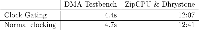
So, let’s be clear today: today’s first test was of my AXI DMA test bench, using this ZipCPU branch. I ran the test using Verilator. I controlled the test via an external C++ test script, and for the first test of the DMA only I left the CPU halted the whole time. As I mentioned above, today’s results initially took 4.4s with clock gating enabled and 5.3s without. This test involved primarily gating the ZipCPU.
So why not try gating the DMA? Even better, why not try gating all of the DMAs within the design? That means not only the memory to memory DMA, but also the memory to stream (MM2S), and the stream to memory DMA (S2MM). The logic is easy enough to add–especially since I’ve now worked out the details (shown above) when testing the memory to memory DMA.
So, for a second test using the same repository, I chose to run the ZipCPU in a Verilator based simulation, inside my AXI DMA test bench, gating all three AXI DMAs. As a test case, I ran Dhrystone, and my AXI performance monitor, and configured the CPU for 4kB instruction and data caches.
The results?
Well, let’s just say the results were not what I was expecting or hoping for.
 |
Perhaps the first lesson learned is that this is not how a proper test should be conducted. I spent the entire weekend running tests, examining the results, updating and adjusting the test, and then running the test again. Sure, the DMA test only took about 5s to run, but 1000 rounds of Dhrystone, followed by the simulated serial port outputting the data (this took longer than Dhrystone itself), took about 12 minutes to run. I’d then examine the results, adjust things, and run the test again and again.
I also adjusted a second variable while running the test. Not only did I
turn clock gating
for the DMA’s or the CPU on and off, but I also enabled
or disabled the OPT_LOWPOWER option within the design. OPT_LOWPOWER is
the name of a parameter that I’ve started adding to many of my designs.
When set, the design will use extra logic to either pin values at zero or
keep them from toggling when not used. A classic example might be AXI_AxADDR.
If AXI_AxVALID is low, why should AXI_AxADDR change?
Much to my surprise, turning on and off the OPT_LOWPOWER option had more of
an effect on my simulations than the clock gate.
| OPT_LOWPOWER=0 (Unused) | OPT_LOWPOWER=1 (active) |
|---|---|
 |  |
Indeed, in the final analysis my clock gating work didn’t have much of an impact on my simulations at all.
So what lessons can we draw from these tests?
-
I was not able to demonstrate any significant simulation time benefit to be gained by clock gating. Sure, 5-6% is measurable and it was eventually consistent, but it’s not really anything to write home about. This itself was a bit of a disappointment, as I was hoping to reproduce that 20% improvement in a larger design with a more complex simulation and I wasn’t able to do so.
-
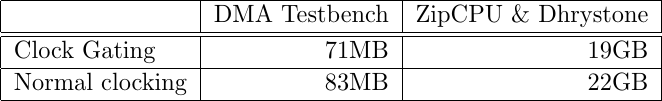
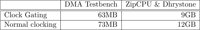
VCD file size appears to be a reasonable proxy for energy used by a design.
This works because a VCD file contains only changed signals. Signals are only written into the VCD file when they change. Signals that don’t change are never updated. As a result, if only one small portion of a design is changing, the impact of the rest of the design on the VCD file size can be very small.
This isn’t a perfect proxy, however, since some signals such as clocks have a greater capacitance, and therefore a greater energy usage within a design than others. Still, VCD file size can be a useful indicator.
-
It can be easier to gate a clock than it is to properly audit your design for toggling signals that don’t need to be toggling. In other words, one might argue that clock gating can be used as a poor man’s substitute for good low power design practice.
-
My two AXI caches [1] [2], together with my AXI to AXI-lite bridge, all needed some low power work since they were allowing a lot of signals to toggle unnecessarily. Indeed, even though my brand new AXI performance monitor had a low power option, I hadn’t yet enabled it.
Worse, my AXI data cache didn’t initially work with
OPT_LOWPOWERset. Under certain circumstances, it would issue a read of a zero address,M_AXI_ARADDR == 0, simply because I had tested fori_op[0](a write operation) instead of!i_op[0](a read operation). This seems to be a common, and rather frustrating problem, where I’ll check a design component into my repository without verifying all of it. I then pull it out later to use it, configure it in a way it hasn’t yet been tested for, expect it to “just work” and then find myself debugging the entire design in order to find and fix an unexpectedly broken component within it. -
The ZipCPU itself needed some low power work. Specifically, the multiplies were always turned on and calculating–even if the CPU was ignoring their results. Similarly, the early branching address and the simulation instruction details were always calculated–even when the CPU wasn’t branching and the simulation instruction wasn’t active.
These things are easy enough to fix, but you won’t recognize they are a problem if you aren’t looking for them in the first place.
-
Small changes tended to have a big impact on the VCD file size. For example, I started with a rough 15GB VCD file size even with clock gating and, through the small number of optimizations listed above, I managed to get that file size down to 9GB.
-
As for design, when designing a component for clock gating it really helps to have access to both the gated and the ungated clock, as well as an ungated signal to tell you whether or not the current clock is gated.
This much cannot be stressed enough. Having access to both sides of the gate was very valuable.
As an example, one of my initial purposes was to examine AXI’s low power interface signals: CSYSREQ, CSYSACK, and CACTIVE. Indeed, one of my earlier clock gating versions of the AXI DMA specifically made use of these signals.
I’ve since ripped all of that logic back out.
Why? First, the AXI specification isn’t very clear on how these signals should be used. Only when digging elsewhere did I discover that these signals are all required to be registered. What good are registered signals, when the only clock you have available to register them with comes from the gated clock domain? A design always needs a way of exiting a low power state, and this is going to require some amount of logic in the ungated clock domain. Second, these signals are supposed to require support from the AXI interconnect, and my interconnect doesn’t (yet) support them. Perhaps I’m missing something. How is the interconnect to know that a bus component is or isn’t busy? Should it always try to shut components down? As a result, until I finally figure out these signals, I’ve torn the capability out. It was just one more item that needed to be maintained, and worse it was rather dubious whether I was accurately supporting the standard at that.
Conclusions
While I’m sure there’s a good reason to use clock gating out there, I’m also pretty sure I haven’t (yet) found it outside of an ASIC context.
-
Clock gating doesn’t appear to have any substantial impact on simulation run time–when using Verilator that is.
-
If you have to allocate a second global clock buffer on an FPGA for a gated clock, then you haven’t really gained much of a power savings–since a large portion of any FPGA design’s power usage will be consumed by the clock buffer.
-
Yes, clock gating can stop registers from toggling. But, let me ask, should those registers have been toggling in the first place? To me, this feels like a cheaters way of handling a bad engineering design. Wouldn’t it be better to simply clean up the design in the first place?
-
That leaves low-power ASIC design as the only remaining reason I can think of for clock gating.
I guess my final conclusion would be that we need to come back to the topic of low power FPGA design on this blog, and deal with it properly and fully at that time. There’s a lot more to low power design than gating clocks, and a review of the tools available to the power conscious FPGA designer could be quite valuable.
And the sun stood still, and the moon stayed, until the people had avenged themselves upon their enemies. Is not this written in the book of Jasher? So the sun stood still in the midst of heaven, and hasted not to go down about a whole day. (Joshua 10:13)