
eMMC Failed. Why?
I often enjoy posting a “bug-of-the week” on X. Following a recent bug post, someone asked me how I found such bugs:
![How do you find these bugs? Are you running simulations or whatever with tests or did you just notice it[?]](/img/emmc-busy/blue-falcon.png) |
So I thought I might share the following story, in illustration of how a bug can be found.
It started a couple weeks ago, when a friend recently pointed me to an Open Source eMMC controller posted by Lattice Semiconductor on GitHub. He asked me for my thoughts.
My first response was, well, gosh, that’s nothing new. I’ve done that already. My next thought was, may God bless them for their hard work. Then, when reading their landing page, I came across a list of not-yet-implemented capabilities. I’ve got all those, I thought, I just haven’t yet demonstrated them on hardware. I’ve proven them in simulation and formal, just not on hardware.
 |
So I responded to my friend with the image in Fig. 1 to discuss our differences. My own eMMC controller, I explained, can handle all of those capabilities that they haven’t yet implemented. The formal proofs all pass, and we have simulations to demonstrate all of them.
The one thing I didn’t have was a hardware demonstration.
But, I had hardware. It’s a new hardware board from PCB Arts, one we are calling the “KlusterLab” board because of all of the capabilities on the board. As of today, it hasn’t been fully tested. (That’s on me, I’m a bit behind on testing this board.) On the other hand, this was a second generation board, so one might expect everything to work–this time.
It was time for an eMMC demonstration.
No, it didn’t work the first time out. Today, I intend to walk through how I found one of the bugs within my eMMC logic.
A Bit of History
The KlusterLab project is funded by NetIdee, as a project called the “Fast Open Switch.” The fundamental capability of the board is a 4-way 10Gb Ethernet switch.
I’ve actually written quite a few posts about this project already. Here’s a quick list:
-
Envisioning the Ultimate I2C Controller discusses the design of the I2C controller used within this design. Although this I2C controller has now been used in other projects, this project tested it against 1) a DDR3 memory stick, 2) reading SFP configuration information, 3) controlling an Si5324 clock generator, 4) HDMI EDID, and 5) an SSD OLED controller.
Here, for example, is a picture of the OLED device showing a set of logos sideways. (Oops) The sideways part was easily fixed–I just don’t have an updated picture on hand. The I2C controller has since been updated for Run-Length Encoding so the instruction set is now much more compact.
 |
As a side note, I started writing a user guide for this I2C controller the last week, only to be surprised at all the details that needed discussion: how the IP works (a topic to be expected), the instruction set it uses, the instruction compiler, the software library associated with it, and more. So this is still coming.
-
The AXI Stream is broken article discusses the problems with AXI Stream, offering a packet based solution that the KlusterLab design follows. This allows the design to drop packets at their boundaries if ever the buffers within the design can’t keep up with them. This also works nicely for CRC detection, allowing the packet to stream through the IP even before CRC detection has completed–something that would be very useful for low–latency networking.
-
What is a Virtual Packet FIFO discusses how to handle storing packets into memory, while also guaranteeing both packet boundaries and that only whole packets will ever go through the buffer.
This IP is anything but low-latency, but that’s another story …
- Using Verilog task to simulate a packet generator for an SDIO controller discusses some of the work that has gone into simulating the eMMC/SDIO controller we’ll be discussing today.
- SDIO RX: Bugs found w/ Formal methods discusses chasing down some bugs we found when first using the eMMC/SDIO controller.
- An Overview of an Ethernet Switch discusses the project as a whole, as well as the basic algorithm bethind the switching.
- Device Clock Generation discusses generating device clocks–something I’ve needed on many projects, to include (again) the same eMMC/SDIO controller we’ll be discussing today.
So we’ve discussed this before. Indeed, one of the things I enjoy about working on open source projects is the ability to discuss them on this blog.
I expected it to “just work”
With all of this background, and given that the eMMC controller worked on the previous version of this board, I didn’t expect any failures when I fired it up and ran my eMMC software test.
Much to my surprised, the eMMC came right up and passed my startup test, but then it failed every subsequent time I ran the same test. If I reloaded the FPGA configuration to the board, then controller would bring the device up again, only to fail again every subsequent time I tested it.
Today, as I’m writing this, it’s been a week or so since it was broken, and so I apologize: I didn’t keep the console log around from when it failed. In general, it would look something like the log in Fig. 3 (taken from a working version).
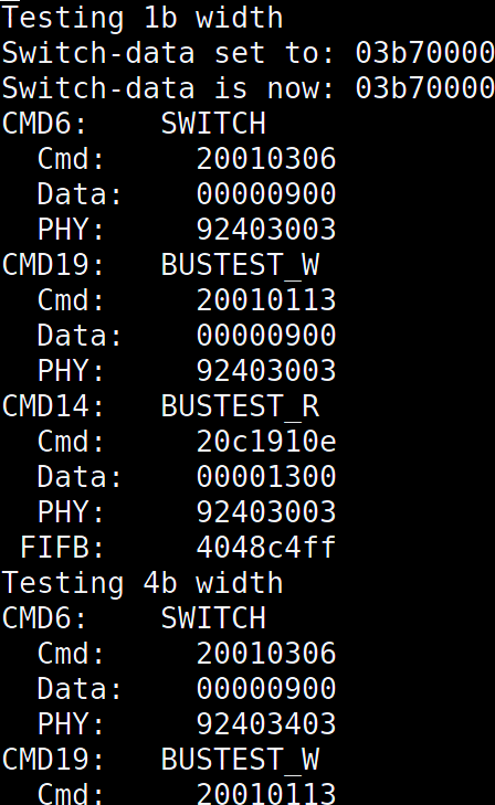 |
The software producing this log may be found in this section of the eMMC software driver. Yes, that’s a “noisy” output in Fig. 3. Yes, it’s easy to get it to be quiet, but when things aren’t working I want the software to be as noisy about what it’s doing as possible–it just makes it easier to debug.
The routine in question is designed to adjust the bus width. The eMMC controller supports 1b, 4b, and 8b data buses. A separate controller, also in the same repository, supports communications over SPI. As per the spec, the controller must start in 1b mode and only transition to 4b or 8b after testing and proving each width. To do this, the driver must go through three steps (all shown in Fig. 3).
-
It must first tell the controller to issue a SWITCH (CMD6) command of the device. This tells the external device (i.e. the eMMC chip itself) to switch bus widths.
For those not familiar with eMMC, commands to the device are all 48b: The first 8b start with 2’b01. The ‘0’ acts as a start bit, whereas the ‘1’ indicates a command issued to the chip. The next six bits are the command itself. We’ll be issuing a CMD6 here, so these 8b will be represented by a 0x46 in hex. These 8b are followed 32b of data, a 7b CRC (automatically added by the controller) and a STOP bit. The command bit then idles high.
The actual physical protocol treats the command wire as a shared wire (in all but SPI modes …). This command wire is pulled up when sending a 1’b1 or grounded to send a 1’b0. At higher speeds, the bus can run in push–pull mode, but for this test we’re still running in this open-drain mode. Indeed, the bottom 8b of the PHY register (8’h03) indicate we’re currently running at 25MHz, and the ‘0’ nibble above that indicate that we’re not yet in push–pull mode.
Once the command has been sent, the controller tristates the command wire to wait for the device to respond. For a SWITCH (CMD6) command, the device responds with a similar 48b response. Other than the fact that this response starts with 2’b00 instead of 2’b01, the response structure is very like the 48b command it is responding to.
Specifically, the SWITCH (CMD6) command is followed what is known within the specification as an “R1b” response. I’ll explain, starting with the “R1” portion. In an “R1” response, the device returns a copy of its internal status register in the 32b bits of data. The “R1b” response additionally has the option to pull bit[0] of the data bus low following this response as an indication that the device is busy responding to this new command.
-
The driver then asks the controller to issue a
BUSTEST_W(CMD19). In the case of aBUSTEST_Wcommand, the controller issues a 48b command and then waits for the 48b response as before. There are two differences. The first is that there’s no busy associated with a CMD14–it just gets a basic “R1” response. The second difference is that theBUSTEST_Wcommand to the controller requests that the controller send 4 bytes of data to the device. This data will be sent over the data pins to the device, once the action on the command pin has completed.When this design failed, the device never responded to the
BUSTEST_W(CMD19) command.The controller went on anyway. Sigh. Good error handling is never the first feature of any design.
-
For the final step, the driver asks the the controller to issue a
BUSTEST_R(CMD14). This command also returns an R1 response (status return only, no busy). Once the reply has been sent, the device then returns the data, using 1b, 4b, or 8b of data lines, it has received in theBUSTEST_Wback to the controller, save that the first two bits on each data line have been swapped. If the return data is as expected, the test succeeds and the bus may use this width.Given that step 2 failed, it should come as no surprise that step 3 also failed.
The design went on anyway. (I do really need some better software error handling …)
So, what do I know? Given that this design worked on the first version of the board, I know that the hardware (i.e. the PCB) works. All the wires are properly connected. Something is still wrong.
Now, how do you find this sort of bug?
Internal Logic Analyzer
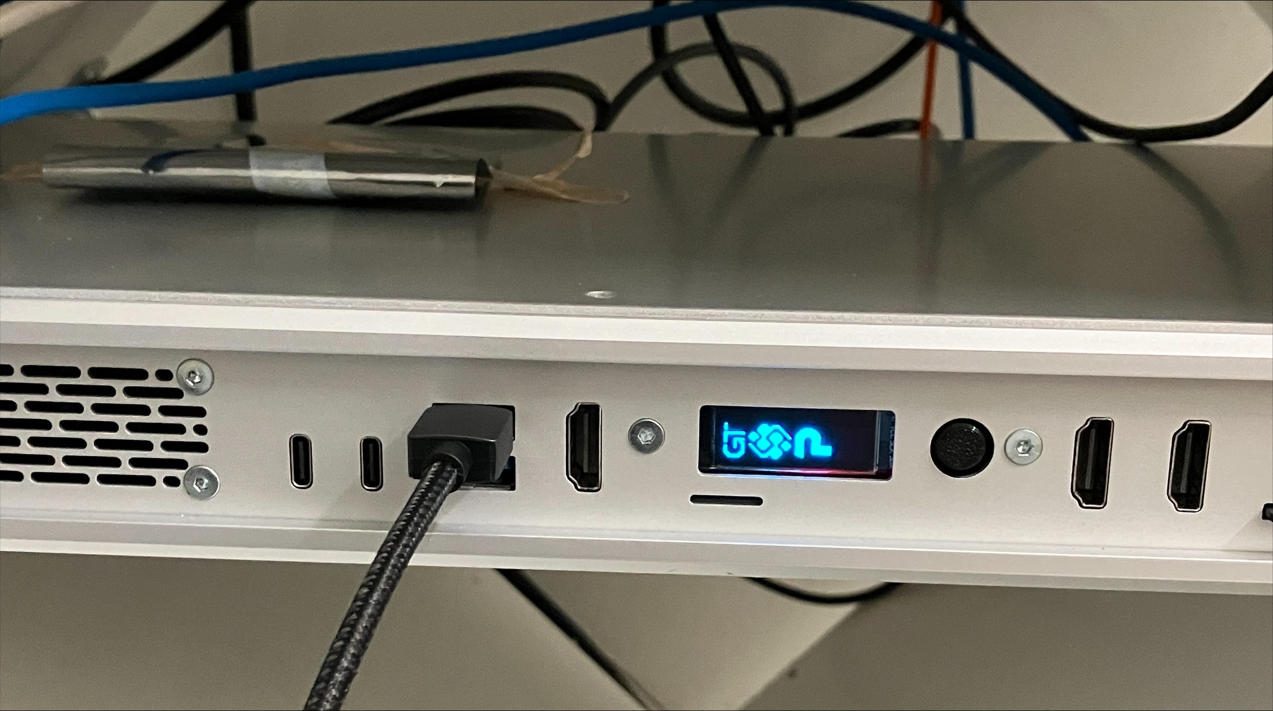
For this, I turn to an internal logic analyzer. AMD(Xilinx) offers an internal logic analysis (ILA) capability as part of Vivado. When I first started working on FPGAs, Xilinx required a separate license to use their ILA. Now I hear they’re going to do it again. In my case, I’m testing this hardware on the other side of the Atlantic Ocean (see Fig. 4 below), from a Raspberry Pi on the KlusterLab board and connected to the FPGA via serial port. (The RPi is also connected to the KlusterLab via an SDIO slave port on the FPGA, but that still needs software to test it.) My point is simply this: I’m not really sure I’d be able to get Vivado to run on this Raspberry Pi, with or without an appropriate license. Instead, I have my compressed Wishbone Scope which I have now used faithfully for many years.
 |
So, how does this get set up? Well, the majority of the work is done by AutoFPGA. Still, let’s take a walk through the key steps.
-
The eMMC controller is first modified to generate 32b of data to be analyzed. When using the compressed version of my Wishbone scope, 31b of these 32 are data of interest while the most significant bit is reserved for a “trigger” that can be used to catch specific items of interest.
As we’ve discussed before, the scope records over a circular buffer. It is always writing to this buffer prior to the trigger. Once it sees the trigger, it waits a user programmed number of clock cycles (known as the “hold off”) before stopping. The scope may also be triggered via software–which is what I did to debug this issue.
In this case, we created a set of debugging outputs from the eMMC Controller’s front end I/O handler.
-
We then create a configuration file for this new “scope”, so that AutoFPGA knows how to connect it to the design. As with most AutoFPGA configurations, this file is primarily a set of copy-paste directions. We also use AutoFPGA’s inheritance feature, and so tell AutoFPGA to configure this eMMC scope like a compressed Wishbone scope, which will itself be configured like a regular Wishbone scope. Therefore, we finally get to the RTL configuration that will be copied/pasted into the design.
We next add this scope’s configuration filename to the AutoFPGA command line.
Now, what happens when we run AutoFPGA?
First, AutoFPGA will paste this RTL into the design.
Next, AutoFPGA will also assign an address, and connect this component to the Wishbone bus. The address is then posted in a register definition file used by any Raspberry Pi (host) helper programs, as well as a more user legible file for use when accessing the device by hand.
Finally, AutoFPGA will build a board definition header file which can then be used by the ZipCPU (or any SOC) to know what components may be accessed, and what addresses to find them at. Specifically, AutoFPGA pasted a description of a WBSCOPE register structure, together with several useful constants into this file. The address of this scope is also pasted into this board description file, so the ZipCPU will know first that it’s there, and second how to find it in the memory space.
The design may now be rebuilt with the scope within it. To remove the scope later, all I will need to do will be to remove the scope’s configuration file name from the AutoFPGA command line.
While this may seem like a lot of steps, the reality is that once the design was originally setup with AutoFPGA, we only needed to adjust three files to add a new scope: 1) we needed to create a scope configuration file to tailor the WBSCOPE’s (already existing) configuration to our purpose. 2) We then needed to adjust the AutoFPGA command line to reference this file. Finally, we 3) ran AutoFPGA to handle all of our bus connectivity and software setup for us.
-
We can now adjust our ZipCPU software. Specifically, we have two macros defined at the top of the driver’s source which are there for this purpose. We just insert
SETSCOPEbefore we expect a bug, andTRIGGERonce we detect the bug.Now, we just run our software to capture any data we can of this bug.
-
The last step is to build a piece of Raspberry Pi software to read this scope’s data back out, and convert it into a VCD file. Thankfully, most of the hard work required to do this is already handled for us. First, we already have a debugging bus that we’ve been using to access our board and load our ZipCPU software onto it. That debugging bus provides us with an easy to use software interface that we can build our control software against. Second, the WBSCOPE repository has a software library that we can use to do the heavy lifting for us. All we need to do is add the definitions of our bits to this library, so we then know how to name the various bits we’ve captured.
Those familiar with AMD(Xilinx)’s ILA might think this to be a lot of steps. I get it. Still, I’m kind of attached to this approach–especially since it works across whatever FPGA chip I might be working with.
With all this as background, we’ve now instrumented our design and we can come back and look at what happened.
What did the scope reveal?
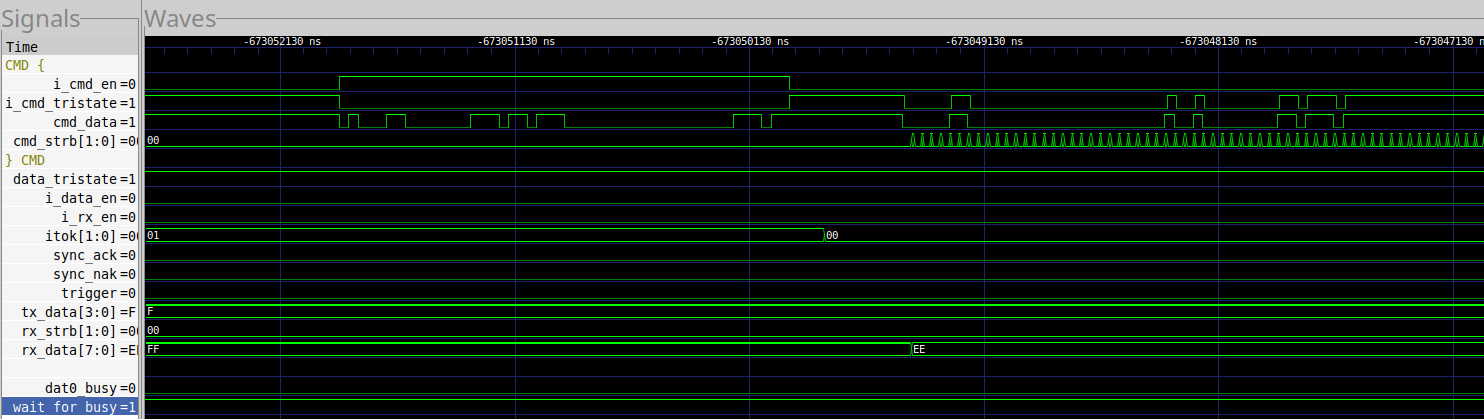
Given that the design was broken, it didn’t take long to get a capture from the scope. Here, you can see the first view of this capture in Fig. 5, shown as a cut of a screen shot using GTKWave.
 |
Wow! 674ms of data, sampled at 100MHz captured in just 4096 four-byte words of RAM? I love this compressed Wishbone scope! (Yes, that is milliseconds, not microseconds or nanoseconds, but milliseconds.) Yes, this is one of those reasons why I like my ILA better than other ones.
What did this capture show us? We’ll have to zoom in a bit to see more of what’s going on. Therefore, let’s take a look at Fig. 6.
 |
At this level, we can see three things going on. First, there’s a burst
of (something) on the command line, followed by a second burst, followed by
itok changing later.
Let’s dig deeper and look at the first burst from Fig. 6 in Fig. 7.
 |
This looks like what we’re expecting. We send a CMD6, followed by a 32b
value and then let up on the bus i_cmd_en=0. The device then responds as
expected.
Just for reference, you can see the same thing in Fig. 8, save that I’ve highlighted key portions of the trace to examine.
 |
This all looks reasonable. You can even read the command and response data off of the command wire if you’d like–just to verify the IP is doing what it says it’s doing.
Also notice the itok value switching to 0. This is our indication that the
device has become busy.
Again, everything looks good here.
Now let’s look at the other burst in Fig. 9.
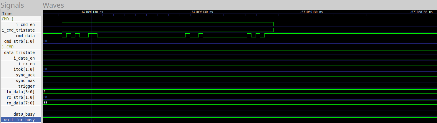 |
This is the command that failed. What’s the first thing we notice? The device never responded!
Let me highlight the difference in Fig. 10.
 |
Why not?
Let’s go back to Fig. 6, and look at those itok bits. These are supposed to
be copies of the data bit zero. These two bits, therefore, are capturing the
devices busy status. Notice how they go to zero following the CMD6? That’s
what we expect from an R1b command (R1 command, with a busy response).
However, our IP is supposed to be waiting on that busy.
So, I went back and added two more lines to the trace. These are the ones
shown at the bottom, already marked as dat0_busy and wait_for_busy. (It’s
not uncommon to need to come back and add more data to a scope, once you know
what you are looking for.) These give us insight into the logic within the
eMMC front end used for calculating whether or not to tell the design the
device is busy.
What I learned (from the broken design), was that the wait_for_busy line
was constantly high, never acknowledging the fact that the DAT[0] line
had gone to zero. Looking at this
logic,
you need to remember that this used to work. It hasn’t been changed since
it last worked. Judging from the trace, it should’ve still worked. Why
wasn’t it working?
Most of the signals used in this logic
block
were things I already had in my trace–or at least things I could infer.
The only one missing was pending_ack. This signal … needed to chang–in
order to support
eMMC BOOT.
Let’s pause a minute to discuss the BOOT protocol. First, there are two types of boot requests. I’ll start with the original one, but the design (is supposed to) support this normal boot request as well as an “alternate” form of boot request. In the case of this boot option, the controller holds the CMD wire low after a reset. It then (optionally) waits for a BOOT acknowledgment token from the device. (I have the IP set up to wait, so the option is enabled.) Eventually, the device will start sending block upon block of data to the IP. Once a pre-programmed number of blocks has been received, the IP will raise the CMD wire and end the BOOT mode.
Fig. 11 shows a basic diagram of what this protocol is supposed to look like.
 |
At least, this is my understanding of the protocol from reading the eMMC specification. Given that BOOT isn’t (quite yet) working, I may not yet have it right.
The point, as far as this bug was concerned, is that this lead me to realize that the IP was waiting for a boot acknowledgement token. Nothing but a (boot) acknowledgment token would ever release the IP from this state! On the other hand, I had since reset the IP (but not this block), so I could move on from the (not yet working BOOT mode) and … this was now preventing me from moving forward.
At this point, all the hard work was done. A simple and quick fix was all that was required: I adjusted the block so that it now “reset” if any data was ever sent or received. That was enough. The bug had now been found and fixed.
Cost Analysis
A lot of people will say hardware is “hard.” It is “expensive.” Let’s understand what kind of “expense” was involved in finding this bug.
First, we’ll start out by being thankful this is an FPGA project. An FPGA design can be debugged and fixed in a day (or longer). An ASIC design might be debugged in a day, but respinning an ASIC without whatever bug is found will cost $10M+ and another six months to a year–in addition to any engineer time, which tends to fall out into the noise.
Second, note what it took to set this up: it took an entire debugging
infrastructure. Unlike software, you cannot simply printf your way out
of a hardware bug like this. You have to build the hardware that will then
give you insight into what’s going on. That takes time. It also costs area
on the FPGA. In my case, most of that time was spent years ago, and all
that was required was adding my
basic scope.
to the design.
Third, it costs time waiting for a design to synthesize. In the case of the KlusterLab, it can currently rebuild with any changes you might add in between a half to a full hour. Thats one hour to add the scope, another hour to adjust it to look at something relevant, and then another hour to figure out what was going on. Finally, it takes another hour to propose and test a change.
So, for a fix that probably did little more than adjust how a couple wires within an FPGA were routed to a single LUT6, this cost a half a day of labour. Thankfully, this is the cost of finding one of the cheaper bugs I’ve had to deal with.
Finally, I haven’t included the cost of the board or its development in this measure.
Now, ask yourself, how easy (or hard) would this have been to debug using either formal verification or simulation tools? 5 minutes? 30? That, my friends, is why debugging in hardware is expensive.
Conclusion
As I write this today, my wonderful eMMC BOOT capability still isn’t working in hardware. Sigh. It should be.
- The eMMC BOOT capability passes a formal verification check
- It passes simulation.
- It’s just not passing hardware yet.
It’s not all bad news. The design now works in HS200 mode (200MBytes/s), and it has worked at least once in HS400 (400MB/s) mode. That’s enough that I’m going to color some of my to-do boxes green–but not really enough that I can use HS400 reliably yet.
Getting the rest of these capabililities up and running at this point is just a matter of time. To get these last capabilities up and running, I’ll be adjusting my scopes. Looking at what is (and isn’t working), making changes, and then testing again.
Likely along the way I’ll discover that I misunderstood some eMMC requirement somewhere, and then did a very good job of implementing the wrong thing. Once I know what I did wrong, I’ll be able to fix it. Then I’ll go back and adjust my formal proofs and simulations to make sure my test suite truly does match the eMMC specification.
But let every man prove his own work, and then shall he have rejoicing in himself alone, and not another. (Gal 6:4)