
Using a Verilog task to simulate a packet generator for an SDIO controller
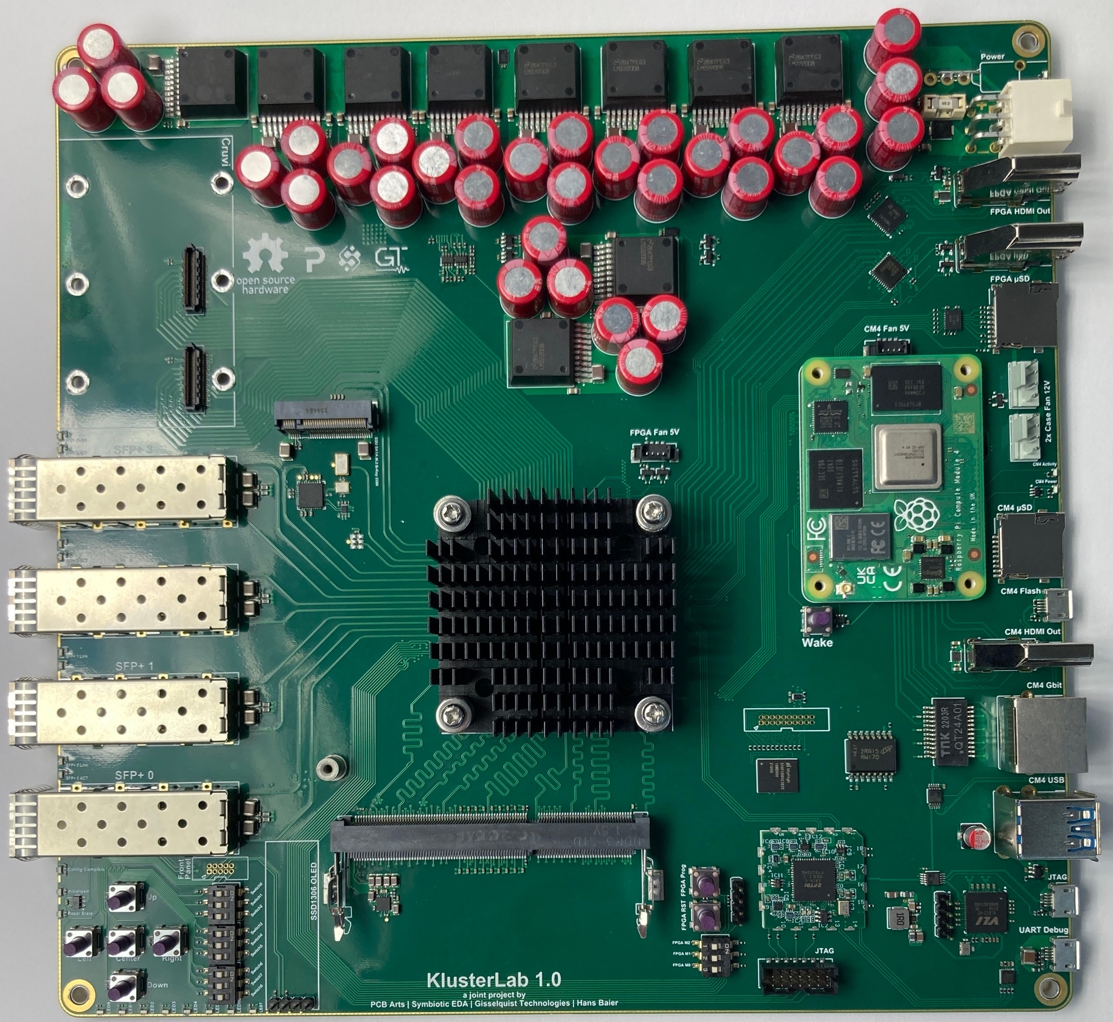 |
One of my current projects is to test and bring up a 10Gb Ethernet test board. The board has been fondly named the “KlusterLab”, because of all of the various interfaces present on it. Among those interfaces are an SD port and an eMMC port. Now, how shall I verify their functionality?
Building an SDIO/eMMC Controller
My first round of testing the SD port used my SPI-based SD card controller, SDSPI. Using that controller, the card responded in much the way I expected, save that the first sector of the card wasn’t what FATFS was expecting. Since this is simply board bringup, where we are just trying to verify that the hardware is working, I signed the component off as working. I could obviously write to the device, and I could read from the device. (Okay, I signed it off too early, but we’re getting there.)
The eMMC port, however, that was going to require more work. I didn’t have an eMMC controller.
On the other hand, I had the beginning scribbles of an SDIO controller I’d started to work on years earlier. SDIO is actually the native SD card protocol. It includes a clock, a bidirectional command wire, and four bidirectional data wires that can be used to send blocks of memory back and forth. Moreover, it the SDIO and eMMC protocols are electrically so similar that a single hardware controller can work for both of them–even if they would need different software drivers. Still, maybe I could breathe some life into my draft controller components?
In the end, I didn’t breathe life into any dead corpse of a project. I pretty much started over.
 |
Why? Well, I figured, if I was going to build a new controller, I should build a design to support all of the IO modes used by eMMC and SDIO. This meant I wanted to support both the open-drain IO these interfaces start out at, as well as their faster push-pull speeds. I wanted to support the bidirectional command and data pins. Since the ports will work with either 1, 4, or 8 (eMMC only) data pins, I wanted to support all of these modes. Finally, the clock speed could run anywhere from 100kHz at the slowest, all the way up to 200MHz. The faster protocols even ran in DDR mode, with the fastest protocol requiring return data capture using a data strobe.
Thankfully, this is all doable. It just needs a little planning.
Over the course of a weekend or two, I managed to draft all of the components to the entire controller. You can see the various parts and pieces of this new controller in Fig. 3 below.
 |
Once I built the front end hardware, I realized I couldn’t use an OSERDES with the FPGAs CCLK pin, so I had to rebuild it without IO elements. I then built it again using DDR elements, and then built it again without Xilinx IO elements at all.
 |
The first front end I built was for the highest speed modes. This was to handle anything above 50MHz, and it did so using both 8:1 OSERDES and 1:8 ISERDES elements. I allowed the return data path to be captured any number of 1.25ns intervals from an outgoing clock edge (when not using the data strobe). Even better, all of the data strobe qualified signals were placed nicely into appropriate asynchronous buffers. Then I realized, the current version of the board will drive the eMMC clock through the CCLK pin, so I have no access to the OSERDES when driving this pin. Hence I built a second version of the front end that just did direct IO pin control–allowing nothing to move at less than a clock cycle and limiting the controller to 50MHz. This I built both with and without Xilinx IO support–to make sure I could handle the speeds CCLK would generate. The final version, shown as #2 in Fig. 4, was a DDR based version. This allowed me to run at 50MHz DDR from a 100MHz primary clock. It also allowed me to simulate something quickly without needing to simulate Xilinx primitives.
(I know, Xilinx primitives aren’t all that hard to simulate in Vivado. In fact, they’re pretty easy to simulate. However, I was using open source tools up to that point and wasn’t yet ready to fire Vivado up.)
All that remained was to verify the controller worked.
But, hey, why let that stand in the way of progress if you have hardware available to you? I mean, look at it this way, properly verifying this brand new controller would require I have a simulation model of an SD Card. Proper simulation models take at least as much time to develop as the IP itself, whereas in this case I have an actual SD card to test against. Why not test against reality?
So, I did.
 |
As you might expect, nothing worked. I wasn’t really all that surprised. Indeed, I sort of expected that. (I’m not really a miracle worker …) What I wasn’t expecting was the controller to fail as early as when the board first came up. That was kind of embarrassing.
The problem was even worse than that.
 |
My whole goal at this portion of the project was to tell if the PCB design had bugs in it or not. Since I had no confidence in my own controller, I couldn’t tell. Was it my controller failing or the PCB?
Even more embarrassing was that I couldn’t read known constant values back from my own controller’s Wishbone registers. You’d think after all these years I could draft a Wishbone register handler and get it right on the first try. (I certainly thought so.) Nope. I didn’t even get that part right. Reading a register which was supposed to have a 4’hc in bits [31:28] returned 4’h0 for those bits. Writing to that register didn’t have any effect. Frankly, I had no idea what the IP was doing when I wrote to or read from it. Yikes!
So that left me in the middle of the longer, slower process of verifying the various components of this IP. I’ve made some progress at this task, and so I now have formal proofs for the divided clock generator, the Wishbone controller and the command pin processor. The proofs aren’t complete, but they were enough to get me moving a step closer to success. They were also enough to find some rather embarrassing bugs–like writing when I was supposed to be reading, or not setting the output register properly at all. That said, I can (now) read and write registers like I expect to, even when testing in hardware(–now). It’s for this reason that I colored these components in green in Fig. 3 above.
Unfortunately, when I got to verifying the packet transmit component, I ran into trouble.
Specifically, I wanted to verify that any packet sent to the packet transmitter would be faithfully forwarded to the front end, with a proper start bit, CRC(s), and stop bit. It needed to do this when transmitting 1bit, 2bits, 4bits, 8bits, 16bits, or 32bits per clock cycle. However, once I got to the point where the controller “passed” its formal induction proof, I switched to checking cover traces and the formal solver couldn’t demonstrate the ability to complete a packet at all. Something in my logic was broken, and cover checks are horrible for not telling you what the problem is.
I needed to switch to simulation.
This, now, is the background behind what I’m going to discuss next.
Simulation Tasks
A full and proper Verilog simulation test bench, such as the one shown in Fig. 7, contains several specific components. These include:
 |
-
A test bench environment. This is the “top level” of the simulated design. All other components will be submodules of this one. The top level test bench will typically define any and all clocks and resets used by the design.
-
The device under test (DUT). In this case, it would be my new controller with all of its pieces.
-
A bus functional model (BFM) to send commands to the DUT. This is one of those build once use everywhere kinds of components. In this case, it would need to be a Wishbone BFM, since this controller has a Wishbone interface. Indeed, I have such a model that I use often when controlling a design from Verilator. I just don’t (yet) have a Verilog one–and the ZipCPU doesn’t really count, although I have used it for that purpose in the past.
-
A device hardware model. This would model the component you intend to communicate with. In this case, it would model either an eMMC or an SD card. It’s also going to be the most complex piece of all the components I’m discussing here, since it will need to support all of the IO modes used by the DUT, as well as responding autonomously to the DUT–just like and SD card or eMMC chip would.
-
The final component of a test bench is a test script, designed to drive the BFM so that it tests the DUT from the perspective of the user.
I’ve learned that this portion of the test really needs to be in its own file. That way, you can swap which test script you run from one test to the next and verify and test different portions of the design at a time.
I colored the missing pieces as black in Fig. 7 above. Unlike the draft and untrusted components I often draw in red, these components haven’t even been drafted.
 |
A good test bench will also include lots of checks within it, either within the BFM or the device model, in order to make sure everything is done according to protocol at all stages in the process. Any failure in this whole setup should be flagged as a failure (if it isn’t an expected and intended failure), and should then be recorded as a failed test case for later fault analysis.
Putting all these components together takes a lot of work. I just wanted to know if my transmit controller worked, and what was causing its formal cover check to fail.
So I just built a quick and dirty test bench, as shown in Fig. 9.
 |
I then wanted to share a piece of this test bench here, since it uses Verilog tasks and I wanted to point out some key features of using tasks together with AXI streams.
The test bench component I wish to share below is a Verilog task designed to
send a packet, via an AXI stream port, to this transmit controller. Further,
it controls one additional transmit control wire–the transmit enable signal,
tx_en. This is the signal from the
Wishbone
controller to the transmit controller enabling its operation.
Let’s walk through this task.
It starts with a task declaration. The task accepts one parameter: the length of the packet to be transmitted in 32-bit words. (It helps that nothing in either the SDIO or the eMMC protocol will need to transmit or receive something that’s not a multiple of 32-bits.)
task	send_packet(input [8:0] length);
	integer	counter;
begin
As with all Verilog task inputs, or outputs for that matter, they are passed by value. Hence even if this length parameter were to change while the task was operating, the value would remain constant within this environment.
There are two other details of tasks to be noted here. The first is that this is a “static” task. “Automatic” tasks are defined by placing the word “automatic” between the task and its name. “Automatic” tasks get a new set of variables assigned to them every time they are called. Since this task is “static”, however, the “counter” value declared above will be shared across all invocations of it. This will also make it easier to debug, since most Verilog simulators have an option to include these values in their generated traces.
The second thing to note is that this is a task and not a function.
Tasks are great when an operation needs to consume time. As such, they
aren’t always synthesizable, whereas functions can be used to encapsulate
complex but synthesizable operations.
Finally, the integer counter declaration just gives us a register we can
work with. It’s identical to reg signed [31:0] counter, but just a bit
simpler to declare.
We’ll start our task off by initializing all the values we are going to control.
	counter = 0;
	@(posedge clk)
	begin
		tx_en <= 0;
		S_VALID <= 0;
		S_DATA  <= $random;
		S_LAST  <= 0;
	end
No, these values are not declared within the task. This is the task controlling values defined within the task’s external context–something I’ve only seen done in test bench contexts like this one.
Do take careful note that all of these signals going into my DUT are clock synchronous. Clock synchronous inputs should be set on the clock edge, and they should be set using non-blocking assignments.
I come across a lot of designs that don’t do this.
One common approach I find is where an engineer will attempt to set things on the clock edge using blocking assignments, but without referencing the clock itself. These engineers might reason that, since the clock has positive edges every 10ns, they should just set test bench inputs every 10ns. Sadly, this leads to a race condition within the simulator, since the values will either then be set before or after the clock edge and not at the clock edge. Worse, you can’t tell from the trace on which side of the clock edge such values were set on. While I’ve seen this mistake often, the lesson learned here tends to come quickly.
I’ve also seen things where engineers will offset their logic from the clock edge. Perhaps they might transition their signals on the negative edge of the clock. This, however, creates a coherence problem within the design, making debugging a challenge. (Yes, this is still the approach I use with Verilator–it is flawed, and I am likely to change how I handle such things in the future.)
In one recent project I worked on, however, I did find that I needed to model the hold time following the clock edge. This was due to the partial modeling of physical realities, to the point where the clock was arriving at multiple times during the clock cycle. My solution to this problem was to add a hold time model, such as:
	@(posedge clk)
	begin
		tx_en   <= #HOLD_TIME 0;
		S_VALID <= #HOLD_TIME 0;
		S_DATA  <= #HOLD_TIME $random;
		S_LAST  <= #HOLD_TIME 0;
	end
Had the right hand side of any of these expressions required calculation
with the current (before clock) data, this would guarantee that the correct
calculation was made, and the correct value set #HOLD_TIME time units
following the clock edge.
As a last note, let me point out that tx_en and S_VALID really need to
already be clear (zero) coming into this routine. Otherwise, if they were
not, it is possible we might’ve just broken the AXI protocol by lowering
S_VALID without checking S_READY.
Now that we have this setup behind us, we can start up the DUT. The first step is to enable the transmitter. Then one clock later, we’ll start the packet stream.
	@(posedge clk)
		tx_en <= 1;
	@(posedge clk)
		S_VALID <= 1;
Why wait a clock cycle? Simply because the actual packet generator will
take a clock cycle (or two) to read from its local block RAM before setting
the S_VALID signal. That’s just the way this particular controller works.
The next step is to send the packet data.
When using AXI streams, there are only two times when you are allowed to set or adjust any stream values. The first is on a reset, when the VALID signal must be brought low. Ever after that, stream information may only be adjusted when either valid is low (which it won’t be here) or when ready is high. Hence, we check for these conditions before adjusting anything.
	do begin
		@(posedge clk)
		if (!S_VALID || S_READY)
		begin
			S_VALID <= !S_LAST;
			S_DATA  <= $random;
			S_LAST  <= (counter+1) >= length;
			counter <= counter + 1;
		end

		wait(!clk);
	end while(counter < length);
Checking for S_READY is very important for this controller. Depending
on the IO settings, the transmitter might be able to send 32 bits per clock
cycle (i.e. 200MHz eMMC clock, 8 data lines, and DDR mode driven from a 100MHz
bus clock), or it might take 32,000 cycles to send 32-bits (i.e. 100kHz clock,
1 data line, and SDR mode), or any number of possibilities in between.
The trick, however, is that we need to keep running this loop until all
data words have been sent. If only sometimes through the loop the data
is accepted, then we need to make sure we keep looping–hence the while
counter < length condition.
But what about the wait(!clk) condition?
That’s there because the non-blocking statements above don’t take any
simulation time. You need to get past them to a point where the simulation
is forced to step forward for the statements above to take effect. If we
didn’t have this wait condition, we might find ourselves looping back up
to the @(posedge clk) statement before our assignments had taken effect.
Waiting for the clock to become negative breaks this cycle, and doesn’t
really effect anything otherwise.
Once all the data has been sent, there’s one more important step: clearing
S_VALID at the end of the packet.
	do begin
		@(posedge clk)
		if (S_READY)
			S_VALID <= 0;

		wait(!clk);
	end while(S_VALID);
The rest of this task is just simulation maintenance. For example, you don’t want to return from sending a packet while the transmitter is still busy, so we’ll wait for it to finish it’s task.
wait(!tx_valid);Once the transmitter completes its task, we need to drop the transmit enable line. We’ll wait a clock cycle first. Then, we have to drop it on a clock edge, since this is a source synchronous signal.
	@(posedge clk);
	@(posedge clk)
		tx_en <= 1'b0;
Lest we allow the controller to start immediately with the next packet, we’ll force a minimum packet separation of another two clock cycles.
	@(posedge clk);
	@(posedge clk);
end endtask
This was enough to stimulate the DUT into sending a packet. It was also enough to find out why the cover check was failing–so I can now return to my formal proof.
It wasn’t enough to check that the packet CRC was valid.
CRC checking can be a challenge with formal methods, so I wanted to check it via simulation anyway. Worse, there are many types of CRCs I need to check. Specifically, both SDIO and eMMC protocol place CRCs at the end of every packet, and those CRCs are one per data line. That’s right. The CRC on data line zero covers only the data on data line zero. The CRC on data line 7 covers the data transmitted on data line 7. Moreover, when working in one of the DDR modes, the CRC checks are split between the two clock edges. There’s one CRC per data line per clock edge, so up to a maximum of 16 CRCs that can be transmitted and then must be checked.
Did I find bugs? Definitely. How many? Too many for my ego. I was convinced I had a wonderful design, with only a few minor bugs before going through this effort. Those “few minor” bugs, however, were causing the transmitter to lock up mid operation–something my formal proof wasn’t catching. This simulation, however, caught the bug nicely.
Unfortunately, because this was an ad-hoc simulation setup, it fails several of the criteria of a “good” simulation. For example, most of the verification that took place was done by looking over the resulting trace. It wasn’t until I got to CRC checking that I started adding assertions to my simulation to automatically catch and flag bugs. As a result, while this helped me get further along in the project, it’s not really good enough to keep around long term.
Conclusion
So, did I find the initial failure? Absolutely! The design came up broken because … the PCB design was broken. The PCB design used an approach to crossing from 1.8V to 3.3V that didn’t allow open drain signals to cross properly. As a result, once I had confidence that my IP was working, I could tell that when the board started up it didn’t pull the data lines high through the voltage translator. Instead, the voltage translator sampled the line low and maintained it at a low level in spite of the pull up resistors that were intended to pull it high. As a result, when the SD card processed the first command I sent, it would notice that data line 3 was also low, and it would go into SPI mode even if I wanted it to stay in SDIO mode.
Yes, that’s right, it’s not just the SDIO controller that is a work in progress, and I’m not the only one who makes mistakes when bringing things up for the first time.
If this is a piece of IP you are interested in, then watch this space. I intend to post it and maintain it there once I’m done getting it to work. Once done, it will have an interface similar to the SDSPI controller that’s currently there, and I intend to maintain the two alongside each other. The two big improvements I’d still like to make are 1) adding a DMA, to push data around to and from memory at the full speed of the bus, and 2) I’d also like to add support for reading or writing a stream of blocks in a row–something the SDSPI controller has no ability to do.
If you are too impatient to wait, you can take a peek at the controller under development here, but I’d caution you that if I were to offer any guarantees or warranties at this point, it would be that there are still bugs in the design. Frankly, it’s a work in progress.
I am tempted, though, to come back to this controller later and write another article about how to process the data strobe returned by the eMMC controller. Such data strobes are becoming commonplace in high speed memory controllers, to such an extent that I’ve now had to build controllers that could handle data strobes from NOR flash (xSPI protocol), HyperRAM, NAND flash (ONFI), and now this eMMC interface. Another project I’m involved in, where I’m only mentoring an amazing engineer, is that of a Verilog DDR3 controller and the DDR3 protocol includes return strobes as well. All told, I may have now seen four or five different ways of processing these return data strobe signals–so it might be ripe for a future blog post and/or a discussion on the topic.
Give instruction to a wise man, and he will be yet wiser: teach a just man, and he will increase in learning. (Prov 9:9)