
Device Clock Generation
After building a CPU, utilities for handling bus interconnects, several DMAs and memory controllers, I often find my time focused on building interfaces between designs and external peripherals. This seems to be where most of the business has landed for me. Often, these peripherals require a clock output, coming from the design, and so I’d like to spend some time describing how to generate such a “device” clock.
 |
There’s actually two topics that need to be discussed when working with modern high speed peripheral design. One of them is generating the clock to be sent to the peripheral, such as Fig. 1 above illustrates. The second one involves processing a clock returned from the peripheral, as shown in Fig. 2 below. This is a key component of high speed designs such as DDR memories, eMMC, HyperRAM, or even NAND flash protocols. This second topic is one we shall need to come back to at a later date.
 |
Today, I’d like to discuss how to go about generating a clock to control device interaction.
I first came across this problem when building a NOR flash controller, based on first a SPI interface and later a Quad SPI interface. My controller was designed for FPGAs, and so the clock could be built with a single frequency. This design had the added complication that the clock needed to be paused from time to time. Specifically, the clock needed to be turned off when nothing was going on. Likewise, the clock needed to be turned off for one cycle after dropping (i.e. activating) the chip select pin, and for a couple cycles after the transaction was complete but before raising (deactivating) the chip select.
I had to deal with a similar problem when controlling a HyperRAM, but … that design failed when I wasn’t (yet) prepared to handle the return clock properly. I did say this deserved an article in its own right, did I not? Processing data on a return clock properly can be a challenge.
I then built a similar design for ASIC platforms. Unlike the FPGA, the final clock speed wouldn’t be known until run time. It might be that the design started at a slower clock speed, only to later speed up to the full rate at run time. Unlike an FPGA which can be fixed later, there’s really no room for failure in ASIC work. At least with an FPGA, if my board didn’t support a particular frequency, I could just rebuild the design for the clock frequency it did support. This doesn’t work, though, for an ASIC–since it tends to be cost prohibitive to rebuild the design at a later time when you decide to connect it to a slower part than the one you designed it for.
The next design I worked with was a NAND flash design. NAND flash can be a challenge, since the protocol requires you to start at a slow frequency and only after you bring up the connection are you allowed to change to a faster frequency. This particular design was built for ASIC environments, and so it depended upon an analog component generating all the clocks I needed. This worked great, up until someone wanted to purchase the design to work on an FPGA, then another wanted it to work on an FPGA, and another and so on.
| SDR |
|---|
 |
| DDR |
 |
Just to add another twist to the problem, many protocols require data transitions on both edges of the clock, a protocol often known as “Dual Data Rate” (DDR). Unlike the other designs above, these often require a clock that is 90 degrees offset from the data–so that each clock transition takes place in the middle of each data valid window, rather than on the edges of the window. This sort of “offset” clock is necessary to guarantee setup and hold times within the slave peripheral. An example of the clock and data relationship required by DDR as opposed to a traditional “single data rate” (SDR) clock is shown in Fig. 3.
By the time I got to my SDIO/eMMC controller, I think I finally had the clock division problem handled. An SDIO controller needs bring up the SD card at 400kHz, and then depending upon the card, the PCB, and the controller, the speed may then be raised to 25MHz, 50MHz, 100MHz, or even 200MHz. The clock may also be stopped whenever either there’s nothing to send or receive, or when the SOC can’t load or unload the data to the controller. For example, you might ask an SD card to read and thus produce many blocks of data, then read the first two of these blocks into your internal buffers only to find that the CPU is slow in draining those buffers. In that case, you would need to stop the interface clock before the external card tries to send you a third block of data that would have nowhere to go.
Other devices require user programmable device clock controllers, such as:
-
10M/100M/1Gb Ethernet controllers
While each of these speeds might use a single clock, building a truly trimode controller requires some extra work.
-
SDRAM controllers from an FPGA standpoint tend to be simple: just produce a clock. However, you can turn the clock off for better power performance. Yes, there are rules … but we won’t get into those here today.
-
I2S
We discussed generating an I2S clock at a totally arbitrary frequency some time ago.
-
In general, I2C is too slow to be the focus of this article. There is an I3C protocol that is built on top of I2C. The techniques we discuss today might work well for I3C masters, but I’m not nearly as familiar with those.
-
While SPI slaves have a device clock as well, handling these clocks is fundamentally different from what I’m describing today. My focus today will be on generating clock signals for the purpose of controlling external devices–such as an SPI master might need to do.
Specifically, today I want to look at and discuss generating a clock with one or more of the following characteristics:
-
Output Signal: We’re talking about interface clocks–those generated by the “master” of the interface. These are digital signals, output from either an FPGA (or ASIC) device.
The output may be accomplished via a component like an ODDR or an OSERDES, with or without an additional analog delay following.
-
Discontinuous: The clock may be discontinuous. Many protocols (flash, SDIO/eMMC, etc) allow or even require, the clock to be stopped, or otherwise only toggled when there’s something to send or receive. As mentioned above, stopping the clock may also be useful for pausing a transmission in progress before a source buffer runs dry, or an incoming buffer overflows.
-
Dynamic Frequency: Often, the outgoing clock needs to change frequency during operation as part of the protocol. For example, the SDIO protocol needs to start at 400kHz, and then increase to 25MHz (or more). Therefore, a good clock generator will need to be able to naturally generate multiple clock frequencies as the protocol requires.
-
Minimum pulse width: Switching between frequencies must be done by rule: clock glitches must be fully disallowed and guaranteed against. Too-short clock pulses cannot be allowed. Clock high and low durations must always be at least a half period of the fastest allowable clock.
-
90 Degree Offset for DDR Signaling: As shown in Fig 3, many modern protocols require both positive and negative edge signaling (DDR). This drops the required clock frequency by 2x, reducing the bandwidth that must be carried over the PCB for the same data rate. However, the clock signal required to support such DDR signaling often needs to be delayed 90 degrees from the data, so that it transitions in the middle of the data valid period.
-
Faster than the controller’s clock: Just to make matters worse, in my eMMC design, I needed to generate a 200MHz DDR device clock from a 100MHz system clock.
All this is to say that our goal today will be to create a divided clock using digital, rather than analog, logic. (Yes, I can hear my analog engineering friends jump in here with the comment that “Everything is analog!” God bless you, my friends.)
The Problem
The first approach I often see to this problem is the straight forward integer clock division approach. Generally, it looks something like the following:
always @(posedge src_clk)
if (reset)
	counter <= 0;
else if (!active_clock)
	counter <= 0;
else // if (active_clock)
	counter <= counter + 1;

assign	dev_clk = (high_speed) ? (src_clk && active_clock)
			: counter[user_selected_bit];
In this case, active_clock controls whether or not the clock is stepping,
and user_selected_bit controls to what level of clock division we are
interested in. As for the src_clk, that can be either the system clock or
alternatively whatever is required to generate the fastest clock frequency
required by the protocol.
Note that we’ve done nothing to guarantee this clock won’t glitch between speed selections, nor can we necessarily guarantee the minimum of two clock rates. We’ll come back to these requirements later, albeit with a different (better) implementation.
The user logic required to use this clock this looks very simple at first:
always @(posedge dev_clk or posedge reset)
if (reset)
begin
	// Reset logic
end else begin
	pedge_data <= // Logic controlling any flops based on the dev_clk
end
When a protocol requires data on both edges of the clock, getting the data right for the second edge of the clock is also important. But, how shall we output data on the negative edge of a clock we’ve just created out of thin air? We’ll need to transition on the negative edge to do this.
always @(negedge dev_clk or posedge reset)
if (reset)
begin
	// Reset logic
end else begin
	nedge_data <= // Logic controlling the negative clock's data
end

assign	output_data = (dev_clk || !ddr_mode) ? pedge_data : nedge_data;
This approach leaves us with two problems. The first is that we’re using our
clock as a logic signal when we assign dev_clk to possible be the same as
our source clock. The second problem is that we are transitioning user logic
on this clock. Worse, though, we’re now transitioning our user logic on both
edges of the clock. This violates the
rules of good
digital logic design.
These aren’t necessarily issues when building ASIC designs. However, in FPGA
design, this clock will need to get onto the clocking network’s backbone
somehow, and that’s not automatic. Worse, this new clock is not the same
as the original src_clk–even when they are at the same frequency. There
will always be a delay between the two clocks–a delay that may not be
captured by pre-synthesis simulation, and so it can be a dangerous delay the
engineer isn’t expecting when building this logic.
This leads to two commercial ASIC design challenges. First, when designing an ASIC IP, you want to be able to test as much of the IP on an FPGA as possible. Non FPGA compatible logic needs to be moved to the periphery of the design and carefully controlled. Second, from a business point of view, it helps to be able to sell the ASIC design to FPGA customers in addition to ASIC customers. So, even though you can do something like this on an ASIC, that doesn’t mean you should.
There are other problems.
-
Since the
src_clkanddev_clkare now two separate and distinct clock domains, you’ll need to properly manage every clock domain crossing between these two clock domains. This can create additional delays through what otherwise might be high speed logic.Likewise, the positive and negative edges of the same clock are also (technically) separate clock domains. Moving between them is “possible, but not recommended.”
-
Gating
You may have noticed we haven’t properly gated our clock above. Sure, we used an
active_clocksignal to provide gating, but this signal does not guarantee the maximum frequency of the output clock. This, however, is a minor problem that most engineers reading this blog would be able to easily fix with a little bit of additional logic.
Two problems in particular, though, become deal breakers when it comes to this
type of design. The first is that DDR interfaces often require a clock delayed
by 90 degrees from the data, as shown in Fig. 3 above. The simple approach
will not generate such a 90 degree delay. While one might use an analog delay
element, such as a Xilinx ODELAY element, to delay the clock signal by an
appropriate amount, this will only work for high speed clocks and not for
clocks less than 50MHz or so. The second problem is, what do you do when you
need a device clock that’s faster than your src_clk, like I did in my
SDIO/eMMC controller design?
As a result, we really need another approach.
The Solution
The basic solution is to return to the rules, and so avoid all transitions on the device clock edge at all. Instead, we’ll continue to transition on our source clock and then use either an ODDR or an OSERDES to generate the final outgoing clock. In the meantime, we’ll treat the newly generated device clock as a traditional logic signal–rather than a “clock” within our design. That is, we’ll let it be and remain logic.
Let’s start by looking at Fig. 3 above, and dividing the clock period into sections, as shown in Fig. 4 below.
 |
Nominally, we’d want at least two sections per clock–one for each piece of data in a DDR transmission. Sadly, this isn’t enough, since the clock might need to be offset by 90 degrees. Hence, we’ll need to break each clock period into four logically distinct time periods. We can label these time periods 3:0, from left-most or most-significant being 3 down to the right most and least significant being 0.
From here, we can generate what I’m going to call a wide clock, four bits at
a time. This wide clock will then be output via a 4:1 OSERDES–if it is to keep
pace with the source clock within our design. At its
fastest speed, this clock will be either 0011 (where the MSB ‘0’ is
transmitted “first”), or 0110 if a 90 degree offset clock is required for
DDR transmissions (as shown in Fig. 4). At its next slowest speed, the clock
would be 0000 followed by 1111, or 0011 followed by 1100. Further
clock divisions will use wide clocks of 0000 or 1111.
If you wish to use an ODDR
instead of a 4:1 OSERDES, you can still use this approach, save that you
would be generating 2 wide clock bits at a time instead of four. The fastest
clock would be a repeating 01, but this fastest clock would be unable to
handle the 90 degree offsets of a DDR signal. The next fastest would be
either 00 followed by 11, or the 90 degree offset version of the same at
01 followed by 10.
If you want a clock running at twice your system frequency, you could use
an eight-bit wide clock signal, designed to feed an 8:1 SERDES. Your fastest
clock would become 00110011 (non–DDR) or 01100110 when working with DDR
signals.
That’s the first step–the wide clock.
The second step is to generate, together with the wide clock signal, two
other signals. The first signal, let’s call this new_edge, will indicate
that a new clock cycle is beginning. The second, which I shall call the
half_edge, will indicate that the second half of a clock cycle is beginning.
Both of these signals are also shown in Fig. 4 above, each indicating the
portion of the clock cycle they represent.
All three of these logic signals can be now generated by a “clock generator” module.
If necessary, this clock can be stopped either at the clock generator, or gated further down the signal pipeline by simply zeroing out the wide clock.
Let’s pause for a moment to illustrate what a “clock” like this might look like.
We’ll start with the highest speed clock, running at the source clock rate.
This clock will have a wide clock of 0011, and new data on every clock edge.
 |
Fig. 5 shows all of these key signals. First, you can see the system clock,
which we called src_clk above, that everything is generated off of. Next, you
can see the IO clock we create, followed by the wide_clock used to create
it. This is followed by the new_edge control signal. This clock might be
the clock we would use for a data signal transitioning at once per clock (SDR).
Therefore, to illustrate, I’ve also illustrated what a couple periods of this
this data signal might look like.
Were this interface to run in DDR mode, sending one word of data on each edge
of the clock, then the wide_clock would need to be (repeatedly) set to
0110, as shown in Fig. 6 below.
 |
There are a couple key differences between Fig. 6 and Fig. 5 above. The first,
and perhaps most obvious, is that the data in Fig. 6 are output at two words
per system clock cycle. This is often desirable, in that twice the data rate
may now be achieved. The second difference is that the IO clock is now offset
90 degrees from the data, instead of 180 degrees. This is often necessary to
guarantee that there is a clock transition in the middle of the data valid
period. To make this happen, the wide_clock is now set to 0110 in each
clock period.
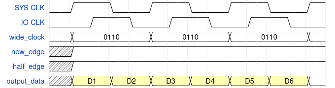
Using these clock signals, we can also pause the clock–as shown in Fig. 7 below.
 |
Note that the key signals, such as new_edge and half_edge must also stop
when the clock pauses (stops). Because there is no clock signal, the data
output signals become don’t care. (For power reasons, I could see holding the
output at at its previous value for short periods of time, D2 in this case,
but that’s another discussion.)
This same signaling approach also works when dividing the clock speed by two. Fig. 8 shows an example SDR signal with a clock speed set to half the system clock speed.
 |
Fig. 9 shows the same thing, but this time for a DDR signal with the clock at half the system clock speed.
 |
Before leaving this example, note how easy it was to change frequencies in
this representation: we just adjusted the wide_clock, and then the new and
half clock positions changed to match.
We can drop the clock frequency again to a quarter of the system clock speed, as shown in Fig. 10.
 |
We can also offset this clock by 90 degrees, as shown in Fig. 11.
 |
When using this type of “wide” clock, user logic becomes simplified as well.
This “simplified” user logic is easily illustrated with an example. For this
example, let’s suppose we wished to control 8 data wires using this type of
divided clock signaling. Let’s also assume, for the purposes of this
illustration, that the source arrives via an AXI stream interface with signals
S_VALID and S_DATA[15:0], and a ready signal given by S_READY.
We’ll start with the wide_clock, new_edge, and half_edge signals from
the clock generator. Note that, as we propagate these signals through our
pipeline (below), we won’t send the wide_clock straight to the output pad,
but instead we’ll use it along side our data processing pipeline. This way,
if the pipeline must stall (and it might need to), the pipeline can also stall
the outgoing clock at the same time.
Hence, we’ll create a one clock delayed version of this wide_clock that
we can call outgoing_clock. Further, a second signal, active_clock,
can be used to keep track of whether or not we’ve committed to the current
clock cycle.
always @(posedge src_clk)
if (i_reset)
begin
	outgoing_clock <= 4'h0;
	active_clock <= 1'b0;
end else if ((S_VALID && S_READY) || (new_edge && second_edge))
begin
	// We commit to this clock if either
	// 1. We have new data and we are ready to consume this new data, *OR*
	// 2. We're in SDR (not DDR) mode, and we've already committed
	//	to a byte of data that we haven't (yet) sent.
	// In both cases, we need to start a clock period.
	//
	// Note that S_READY implies new_edge
	//
	outgoing_clock <= wide_clock;

	// The "active_clock" signal is used to let us know that we've committed
	// to this clock cycle.  From now until the next new_edge, we must
	// forward the wide_clock signal to the output.
	active_clock <= 1;
end else if (new_edge)
begin
	// The clock generator is creating an edge that ... we're not prepared
	// for or ready to handle.  There's just no data available, so ...
	// let's stop the clock.
	outgoing_clock <= 4'h0;

	// In this case, we're not forwarding the clock, nor will we until
	// the next clock period.
	active_clock <= 1'b0;
end else if (active_clock)
	// If we've already committed to this clock cycle, then we'll need to
	// ontinue it to its completion.
	outgoing_clock <= wide_clock;
Before we can get to the data, we need another key signal as well. This is
the second_edge signal that we used above. Here’s why: our data is going to
arrive, 16b at a time via AXI stream. If we are in DDR mode, then we’ll
consume 8b on each edge of this clock–and possibly all 16b at once. However,
if we are only in SDR mode, then we’ll need to consume the second 8b on the
next clock edge. Hence, we’re going to need a signal that I’m calling,
second_edge, to tell us that we have 8b remaining of the 16b committed to us
that didn’t get sent on the last clock tick.
always @(posedge src_clk)
if (reset && i_care_about_resets)
	second_edge   <= 0;
else if (S_VALID && S_READY)
	// In SDR, we just accepted 16b and output 8b.
	// We need another new_edge to send the remaining 8b.
	// Note that S_READY implies new_edge
	//
	// Also note that we only use this signal in SDR modes
	second_edge <= !ddrmode;
else if (new_edge)
	// On any (other) new_edge, we can clear this signal
	second_edge <= 0;
That leads us to the outgoing_data. This is a 16 bit data signal, consisting
of 8b, outgoing_data[15:8], which will be output on the first half of the
clock, and another 8b, outgoing_data[7:0], which will be output on the second
half of the clock. A third signal, next_byte, will be used for keeping track
of the second byte of data in the case where we don’t output both bytes in the
same clock period.
always @(posedge src_clk)
if (reset && i_care_about_resets)
begin
	outgoing_data <= 0;
	next_byte   <= 0;
end else if (S_VALID && S_READY)
begin
	// new_edge is implied by S_READY
	if (ddrmode && half_edge)
	begin
		// Set data for both halves of the clock
		//    The first half in the MSBs
		outgoing_data[15:8] <= S_DATA[15: 8];
		//    The second half in the LSBs
		outgoing_data[ 7:0] <= S_DATA[ 7: 0];

	end else begin
		// Set only the first half ot the data, but set it to be
		// output twice.  We'll need to come back later for the second
		// outgoing byte.
		outgoing_data <= {(2){S_DATA[15:8]}};
	end

	// Keep track of that second byte, so we can come back to it later.
	next_byte <= S_DATA[7:0];
end else if (new_edge ||(ddrmode && half_edge))
begin
	outgoing_data <= {(2){next_byte}};
end
The final signal we need to define is the S_READY signal. In this example,
we can accept new data on any new clock edge, unless we have 8b remaining
from the last clock edge that have yet to be output.
assign S_READY = new_edge && !second_edge;This approach provides us with a couple big advantages to our user logic over what we had before.
First and foremost, all of our user logic now takes place on the same
src_clk.
We didn’t need any CDCs.
AXI slave data, generated externally on this src_clk can now be used within
our design on the same clock it was generated on.
Second, did you notice how we were able to simply gate the
clock when there was no
data available? If not, go back up and look again at the active_clock signal.
Third, unlike the previous approach, we’ve now guaranteed that this clock signal won’t glitch. That is, assuming the outgoing OSERDES won’t generate glitches from our glitchless data signals. The previous clock generator, on the other hand, could well have had glitches between the clock and the data enabling it.
Also look at how easy it was to do pipelined processing. The clock was
generated prior to our pipeline, and simply propagated through the pipeline.
Although this pipeline only contains a single clock cycle, we could’ve easily
extended the pipeline for multiple clock cycles if necessary by simply passing
the wide_clock, new_edge, and half_edge signals through the
pipeline–adjusting them if and where necessary along the way.
As a result of this example, all IO pins can now be driven using a 4:1 OSERDES. (You could also use ODDRs for the data, if you trusted them to have the same timing relationship as the OSERDES.)
What about frequency changes, or adjusting between the unshifted clock and the clock shifted by 90 degrees? What about when the clock is off, and needs to be turned on? All of these challenges and more now reside within the clock generator.
The Clock Generator
For discussion purposes, let’s take a look at the clock generator I used for my SDIO/eMMC controller. As mentioned above, this clock generator has the particular requirement of being able to generate two outgoing clock periods per system clock cycle, but otherwise it’s a fairly straight forward example of the discussion above.
From a configuration standpoint, there are a couple of configuration options. For example, I wasn’t certain that I’d always have an 8:1 SERDES available to me, nor do all digital environments necessarily offer 2:1 ODDR components. Therefore, we allow those to be adjusted. Second, I want to know the maximum number of bits required in my clock divider.
Still, these configuration parameters are fairly straightforward.
module	sdckgen #(
		// OPT_SERDES is required for generating an 8:1 output.
		parameter [0:0]	OPT_SERDES = 0,

		// If no 8:1 SERDES are available, we can still create a clock
		// using a 2:1 ODDR via OPT_DDR
		parameter [0:0]	OPT_DDR = 0,

		// To hit 100kHz from a 100MHz system clock, we'll need to
		// divide our 100MHz clock by 4, and then by another 250.
		// Hence, we'll need Lg(256)-2 bits.  (The first three speed
		// options are special)
		localparam	LGMAXDIV = 8
	) (
The clock generator is primarily controlled via three signals. The first tells us whether we want our clock offset by 90 degrees for DDR outputs or not. The second controls the speed of the outgoing clock. The final signal tells us we can shut the clock down.
		input	wire			i_cfg_clk90,
		input	wire	[LGMAXDIV-1:0]	i_cfg_ckspd,
		input	wire			i_cfg_shutdown,
When shut down, the wide clock output will be fixed at zero, as will both the
new_edge and half_edge control signals.
The shutdown signal is actually really useful at slow clock speeds. Sure you could shut the clock down, as we did above, by just not forwarding it through the pipeline. On the other hand, once the clock has been shut down, you’d like to be able to restart it on a dime. The shutdown control signal to our clock generator allows us to do that. Once set, the clock generator takes the remainder of a clock cycle to shut down, and then stays ready to restart the clock at a moments notice.
The outputs from this module are just about what you would expect. You
have the three signals we’ve already discussed. In this case, o_ckstb
is the new_edge signal we’ve mentioned, o_hlfclk is the
half_edge signal, and o_ckwide is the wide_clock signal.
		//
		output	reg			o_ckstb,	// new_edge
		output	reg			o_hlfck,	// half_edge
		output	reg	[7:0]		o_ckwide,	// wide_clock
		output	wire			o_clk90,
		output	reg	[LGMAXDIV-1:0]	o_ckspd
	);
The two new signals are o_clk90 and o_ckspd. These are feedback signals
returned to the control module,
used to tell us when any frequency shift or phase shift operations are complete.
These feedback signals solve an issue I was having in my eMMC controller, where the clock would be at some crazy low frequency (100kHz or so), and I’d want to speed it up. Just setting the new clock speed wasn’t enough, since it might take a thousand clocks to finish a single cycle at the 100kHz clock speed. However, by checking these return signals via the register set, the software driver could then tell if any clock frequency change had fully taken effect before going on to any next operation.
The next logic block is part of a two process finite state machine. The first process, shown below, is the combinatorial process. The second will be the clocked logic.
Personally, I’m not a big fan of two process state machines. I’m just not. They often seem to me to be adding extra work and complexity. However, two process state machines allow me to reference logic results even before the full logic path is complete. They also allow me an ability to describe more complicated logic than the simple single process state machine, so a two process state machine it is.
In this case, we are going to generate the next signal for the strobe,
nxt_stb, the clock, nxt_clk, and the counter, nxt_counter.
Of these signals, nxt_clk is the simplest to explain. This signal indicates
that we’re about to start a new clock cyle. In many ways, this is the
combinatorial version of what is to become the new_edge once latched.
Clock cycles themselves come in four phases, just like the four bits of the
wide clock we discussed before. You can think of these phases as the 0110
of the fastest clock before. The first bit, 0, is the first phase of the
clock. Our new_edge bit, o_ckstb, will only ever be true on this phase.
The second bit, 1, is where the clock rises. The third bit, 1 again, is
the only phase where the half_edge, o_hlfck, will be set. Finally, the
clock will return to zero in the last phase. If the clock is ever idle,
it will idle in this first phase prior to delivering a new_edge signal.
This background will help explain how I’ve divided up the counter. There are
NCTR bits to the counter. Of those bits, the top two control the phase
bits we just described, whereas the others are the clock divider. The
nxt_stb signal, mentioned above and below, is simply a signal that these top
two phase-control bits are about to change.
With that as background, let’s take a look at how this works.
In general, the first step of any combinatorial block is to set all the values that will be determined within the block. This is a good practice to get into to avoid accidentally generating any latches.
	always @(*)
	begin
		nxt_stb = 1'b0;
		nxt_clk = 1'b0;
		nxt_counter = counter;
From here, we subtract one from the bottom (non-phase) bits of our counter
on every cycle. When these bits are zero, subtracting one will cause the
counter to overflow and set our nxt_stb signal, so we can know when to
adjust the phase bits.
		{ nxt_stb, nxt_counter[NCTR-3:0] } = counter[NCTR-3:0] - 1;

		if (nxt_stb)
		begin
			// Advance the top two bits
			{ nxt_clk, nxt_counter[NCTR-1:NCTR-2] }
						= nxt_counter[NCTR-1:NCTR-2] +1;
If our clock speed is set to 0 (wide clock of either 01100110 or 00110011)
or 1 (wide clock of 00111100 or 00001111), then we are always generating
a new clock cycle. In this case, we’ll hold the counter at zero and (roughly)
ignore the phase.
			if ((OPT_DDR || OPT_SERDES) && ckspd <= 1)
			begin
				nxt_clk = 1;
				nxt_counter[NCTR-3:0] = 0;
Likewise, if the clock speed is equal to two, the wide clock will either
alternate between 0000_0000 and 1111_1111, or 0000_1111 and 1111_0000,
and so our phase will alternate, but otherwise everything else can be kept
to zero.
			end else if (ckspd <= 2)
			begin
				nxt_clk = counter[NCTR-1];
				nxt_counter[NCTR-3:0] = 0;
Finally, in the more general case, we’ll just set the bottom bits to count
down from ckspd-3 to zero. Yes, this is “just” a counter, but the maximum
value is offset by three for the three special speeds we just discussed above.
			end else
				nxt_counter[NCTR-3:0] = ckspd-3;
		end
You may have noticed that we’ve only adjusted the bottom bits of this counter–the bits that count down. We’ve done nothing to update the phase bits at the top of this “counter”, so let’s handle those next. (Spoiler alert: these MSBs don’t act like counter bits in this implementation.)
Of course, for the highest frequencies, the counter will never change. It sits at zero, with a permanent next phase of 3.
		if (nxt_clk)
		begin
			if ((OPT_DDR || OPT_SERDES) && new_ckspd <= 1)
				nxt_counter = {2'b11, {(NCTR-2){1'b0}} };
When the speed setting is 2, we allow the top two bits to toggle back and
forth. If nxt_clk is set, we need to reset these bits only.
			else if (new_ckspd <= 2)
				nxt_counter = { 2'b01, {(NCTR-2){1'b0}} };
Finally, for the general case, we return the phase to zero and reset the clock.
			else begin
				nxt_counter[NCTR-1:NCTR-2] = 0;
			end
		end
	end
This is only the first half of this “two process” FSM. The second half, with respect to the counter, is just about as simple. Perhaps it is even more so, given that we’ve done all of the hard work above.
	always @(posedge i_clk)
	if (i_reset)
	begin
		if (OPT_SERDES)
			counter <= 0;
		else if (OPT_DDR)
			counter <= { 2'b11, {(NCTR-2){1'b0}} };
		else
			counter <= { 2'b01, {(NCTR-2){1'b0}} };
	end else if (nxt_clk && i_cfg_shutdown)
		counter <= { 2'b11, {(NCTR-2){1'b0}} };
	else
		counter <= nxt_counter;
The big thing to notice here is the nxt_clk && i_cfg_shutdown. Remember, if
the user ever asserts i_cfg_shutdown, we need to wait for clock cycle to
complete before shutting it down. Hence, we wait for the nxt_clk signal
before acting. Then, once set, we leave the counter in a state where it
will perpetually set nxt_clk. This way, the moment i_cfg_shutdown is
released, we’ll be back to generating a clock again.
To explain this a bit better, imagine the clock generator is producing
an output clock from ten periods of the source/system clock: five system clocks
of 0000_000, followed by five more clocks of 1111_1111. Imagine
again that we’ve had several periods of these 10 clock cycles before the
user asserts the clock shutdown signal. We then wait another 10 cycles for the
clock to fully shut down. Now, if the user drops the shutdown signal after a
further 3 cycles, we could either wait another 7 cycles (to complete the 10),
or start immediately. Here, we try to arrange to start a stopped clock
immediately without violating any of our clocking rules.
The next signal, clk90, controls whether or not we’re generating an
clock offset from new_edge, o_ckstb, by 90 degrees or not.
	always @(posedge i_clk)
	if (i_reset)
		clk90 <= 0;
	else
		clk90 <= w_clk90;

	assign	o_clk90 = clk90;
This logic isn’t very interesting yet, since we’ve basically split a two
process FSM. It will become more so when we get to w_clk90, and the first
process of the FSM, below. The key is, this logic must determine what the
current 90 degree offset setting is. Hence, when you look at the outgoing
wide clock, this signal must match it.
How about the clock speed? In this case, we go through some error checking.
	initial	ckspd = (OPT_SERDES) ? 8'd0 : (OPT_DDR) ? 8'd1 : 8'd2;
	always @(posedge i_clk)
	if (i_reset)
		ckspd <= (OPT_SERDES) ? 8'd0 : (OPT_DDR) ? 8'd1 : 8'd2;
	else
		ckspd <= w_ckspd;

	always @(*)
	if (OPT_SERDES)
		new_ckspd = i_cfg_ckspd;
	else if (OPT_DDR && i_cfg_ckspd <= 1 && !i_cfg_clk90)
		new_ckspd = 1;
	else if (i_cfg_ckspd <= 2 && (OPT_DDR || !i_cfg_clk90))
		new_ckspd = 2;
	else if (i_cfg_ckspd <= 3)
		new_ckspd = 3;
	else
		new_ckspd = i_cfg_ckspd;

	assign	w_clk90 = (nxt_clk) ? i_cfg_clk90 : clk90;
	assign	w_ckspd = (nxt_clk) ? new_ckspd   : ckspd;
The error checking is here to guarantee that a clock speed of 0 is only used
when OPT_SERDES is set. Likewise, a clock speed of 1 may be used in
ODDR
mode (wide clock of 00001111), but not when the clk90 configuration
is set (calling for a wide clock of 0011_1100 which is too complex for an
ODDR output module to produce).
This continues for a clock speed of two which is fine for a non-offset clock
(wide clock of 0000_0000 followed by 1111_1111), but not for an offset
clock (wide clock of 0000_1111 followed by 1111_0000 unless the OPT_DDR
option is set.
Finally, the two values w_clk90 and w_clkspd are used to tell us what
values our registered logic should use when generating a clock. As such,
they are either the registered values, or (when we’re about to start a new
cycle) the new values.
With all this as background, we can now dig into the core of this logic–generating the three key signals we will be outputting.
On reset, these signals will simply be set to indicate a clock of the
fastest rate, ready to go, but otherewise one that is idle (o_ckwide=0).
	initial	o_ckstb  = 0;
	initial	o_hlfck  = 0;
	initial	o_ckwide = 0;
	always @(posedge i_clk)
	if (i_reset)
	begin
		o_ckstb  <= 0;
		o_hlfck  <= 0;
		o_ckwide <= 0;
Next, if we want to shutdown the clock, we can only do so on nxt_clk.
When shutdown, the wide clock will be zero and the new edge signals willl
all be suppressed.
	end else if (nxt_clk && i_cfg_shutdown)
	begin
		o_ckstb  <= 1'b0;
		o_hlfck  <= 1'b0;
		o_ckwide <= 8'h0;
As mentioned above, the key here is that the clock can suddenly start if
the i_cfg_shutdown signal is released. Using this logic, it does not need
to remain phase coherent with whatever phase the clock had prior to being
shutdown.
Moving on to our highest speed clock, we simply set that according to
the 90 degree clock configuration. In general, this speed will only
ever generate one of two values: 01100110 or 00110011.
	end else if (OPT_SERDES && w_ckspd == 0)
	begin
		o_ckstb  <= 1;
		o_hlfck  <= 1;
		o_ckwide <= (i_cfg_clk90) ? 8'h66 : 8'h33;
When running from a 100MHz system (src_clk) clock, this plus the OSERDES
will generates a 200MHz clock signal to the external device.
One might argue that the OPT_SERDES here is really redundant. There should
be enough logic elsewhere to keep w_ckspd at a non-zero value if OPT_SERDES
is not set. Why use it?
It’s here specifically to provide a strong hint to the synthesis tool
regarding logic that can be cleaned up if OPT_SERDES is not set. This block
is complicated enough as it is, so adding it in should simplify our logic.
The problem with putting this value here, and generating a clock module based
upon parameters such as OPT_SERDES and OPT_DDR, is that I now need to
formally verify the IP under several conditions before I can know if it works.
This applies to simulation as well. It is now no longer sufficient to run
the simulation tool once when you do something like this. It must now be run
many times under different conditions. As an engineer, I need to be aware
of costs like this whenever I invoke logic like this.
In this case, I wanted to support multiple types of FPGAs (and/or ASICs), and so this was the logic I chose.
Our next speed, ckspd=1, has almost the same logic. As before, o_ckstb
and o_hlfck are both set continually in this mode. In this case, our wide
clock output will either be 0011_1100 or 0000_1111 depending on whether
or not we need a 90 degree offset clock for DDR.
	end else if ((OPT_SERDES || OPT_DDR) && w_ckspd <= 1)
	begin
		o_ckstb  <= 1'b1;
		o_hlfck  <= 1'b1;
		o_ckwide <= (OPT_SERDES && w_clk90) ? 8'h3c : 8'h0f;
When running from a 100MHz system (src_clk) clock, this generates a 100MHz
clock as well.
You may note that there’s no real two-cycle output signal. The signaling,
with o_ckstb and o_hlfck, allows us to describe a new clock together
with or separate from the second half of that clock period, but offers nothing
for describing two clock cycles in the same source clock period. This is
just a limitation in our chosen signaling.
The solution to this problem is specific to the eMMC controller that we’ve drawn our example from. In this case, I look at both the DDR setting and the clock speed before generating any transmit data. From this, I determine if I should be sending one byte, two bytes, or four bytes of data per clock. The actual logic is more complex, due to the fact that the eMMC interface may run in 1b, 4b, or 8b modes, but that’s the story of another piece of logic, found outside of the clock controller.
As with clock speeds of either 0 (200MHz) or 1 (100MHz), the clock speed of 2
(50MHz) is also handled specially. This is the speed that alternates between
two outputs, generating either 00001111 followed by 11110000 in the offset
mode (o_clk90=1), or simply 00000000 followed by 11111111 in the normal
mode.
	end else if (w_ckspd == 2)
	begin
		{ o_ckstb, o_hlfck } <= (!nxt_counter[NCTR-1]) ? 2'b10 : 2'b01;
		if (w_clk90 && (OPT_SERDES || OPT_DDR))
			o_ckwide <= (!nxt_counter[NCTR-1]) ? 8'h0f : 8'hf0;
		else
			o_ckwide <= (!nxt_counter[NCTR-1]) ? 8'h00 : 8'hff;
When running from a 100MHz system clock (src_clk above), this generates
a 50MHz output clock signal. This might be the “fastest” speed you would
normally think of for an integer clock “divider”. As you can see, though,
we’ve already generated outgoing 200MHz and 100MHz clocks above.
This brings us to the general case–a divided clock running at less than half
our source clock rate. Here, we’ve already done all of the hard work for
nxt_clk, so the outgoing next edge signal o_ckstb is done.
	end else begin
		o_ckstb <= nxt_clk;
The half edge signal is determined by the counter. The lower bits must be zero, indicating a new phase, and the top two bits indicate the new phase will be the third of four–so just entering halfway.
o_hlfck <= (counter == {2'b01, {(NCTR-2){1'b0}} });The wide clock is determined by the top two phase bits of the next counter. It’s either equal to the most significant bit, when there’s no clock offset, or the exclusive OR of the top two bits when there is.
		if (w_clk90)
			o_ckwide <= {(8){nxt_counter[NCTR-1]
						^ nxt_counter[NCTR-2]}};
		else
			o_ckwide <= {(8){nxt_counter[NCTR-1]}};
	end
This leaves us with only one final signal: the current clock speed. In this case, all the work has been done above, and nothing more need be done with it.
	always @(posedge i_clk)
		o_ckspd <= w_ckspd;
That’s the basic idea. In summary:
-
There are four phases to the outgoing clock, either
0011or0110. -
A counter generally helps us know when to transition from one phase to the next.
-
High speeds get special attention.
-
Data changes on the outgoing next edge signal,
o_ckstb.In DDR modes, data can also change on the outgoing
o_hlfstbsignal.
Key features of this approach include:
-
There’s no need for any clock domain crossings in the outgoing data path. All outgoing signals are handled in the source clock domain.
-
The clock may be gated at will, and (re)started quickly if necessary.
-
Frequency changes are controlled, and will take place between clock periods.
-
Although the clock is generated in logic, it doesn’t trigger any logic. That is, nowhere in the design will anything in the outgoing logic path depend upon either
@(posedge dev_clk)or@(negedge dev_clk). Instead, all of the logic is triggered off of theo_ckstboro_hlfstbsignals while still running on the samesrc_clkwe started from.
But … does it work?
Simulation testing
Just to get this clock generator off the ground, I built a quick simulation test bench. You can find it here, and we’ll walk through it quickly.
The first step was pretty boiler plate. I simply started a VCD trace, placed the design into reset, and generated a 100MHz clock.
	initial begin
		$dumpfile("tb_sdckgen.vcd");
		$dumpvars(0,tb_sdckgen);
		reset = 1'b1;
		clk = 0;
		forever
			#5 clk = !clk;
	end
For the second step, I wanted to place the design in a variety of
configurations to see how it would work in each. I chose to leave it in each
configuration for five clock cycles before moving to the next. I then defined
a simple task, capture_beats, that I could call to wait out five cycles of
a given clock setting before moving on.
	task	capture_beats;
	begin
		repeat(5)
		begin
			wait(w_ckstb);
			@(posedge clk);
		end
	end endtask
The last step, then, was to walk through one clock setting after another to see what would happen.
I started by taking the design out of reset, and configuring the inputs for a (rough) 100kHz clock.
	initial begin
		{ cfg_shutdown, cfg_clk90, cfg_ckspd } = 10'h0fc;
		repeat (5)
			@(posedge clk)
		@(posedge clk)
			reset <= 0;

		// 100kHz (10us)
		capture_beats;
You can pretty well read the comments below to see the configurations I checked.
		// 200 kHz (5us)
		@(posedge clk)
			{ cfg_shutdown, cfg_clk90, cfg_ckspd } = 10'h07f;
		capture_beats;

		// 400 kHz (2.52us)
		@(posedge clk)
			{ cfg_shutdown, cfg_clk90, cfg_ckspd } = 10'h041;
		capture_beats;

		//   1MHz (1us)
		@(posedge clk)
			{ cfg_shutdown, cfg_clk90, cfg_ckspd } = 10'h01b;
		capture_beats;

		//   5MHz (200ns)
		@(posedge clk)
			{ cfg_shutdown, cfg_clk90, cfg_ckspd } = 10'h007;
		capture_beats;

		//  12MHz (80ns)
		@(posedge clk)
			{ cfg_shutdown, cfg_clk90, cfg_ckspd } = 10'h004;
		capture_beats;

		//  25MHz (40ns)
		@(posedge clk)
			{ cfg_shutdown, cfg_clk90, cfg_ckspd } = 10'h003;
		capture_beats;

		//  50MHz (20ns)
		@(posedge clk)
			{ cfg_shutdown, cfg_clk90, cfg_ckspd } = 10'h002;
		capture_beats;

		// 100MHz
		@(posedge clk)
			{ cfg_shutdown, cfg_clk90, cfg_ckspd } = 10'h001;
		capture_beats;

		// 200MHz
		@(posedge clk)
			{ cfg_shutdown, cfg_clk90, cfg_ckspd } = 10'h000;
		capture_beats;


		//  25MHz, CLK90
		@(posedge clk)
			{ cfg_shutdown, cfg_clk90, cfg_ckspd } = 10'h103;
		capture_beats;

		//  25MHz, CLK90
		@(posedge clk)
			{ cfg_shutdown, cfg_clk90, cfg_ckspd } = 10'h102;
		capture_beats;

		// 100MHz, CLK90
		@(posedge clk)
			{ cfg_shutdown, cfg_clk90, cfg_ckspd } = 10'h101;
		capture_beats;

		// 200MHz, CLK90
		@(posedge clk)
			{ cfg_shutdown, cfg_clk90, cfg_ckspd } = 10'h100;
		capture_beats;

		$finish;
	end
These are basically all of the configurations I wanted to use the design with. Using the generated trace, I can visually see all of the signals within this design working as intended. Further, unlike the formal verification we’ll discuss next, I can actually see many clocks of this design. This allows me to verify, for example, that the 100kHz, 200kHz, and 400kHz clock divisions work as designed.
Sadly, this test is woefully inadequate for any real or professional purpose.
The biggest problem with this simple test bench script is that it’s not self checking. I can run it, but the only way to know if the design did the right thing or not is to pull up a viewer and check the VCD file. Sure, this might get me off the ground, but it is horrible for maintenance. How should I know, for example, if a small and otherwise minor change breaks things?
The second problem with this test bench is that it does nothing to try out unreasonable input signals. How shall I know, for example, that this design will never go faster than the fastest allowed frequency? That is, it should only ever be able to go as fast as the current speed, or the newly commanded speed.
Perhaps some of you may remember my comments on twitter about getting excited to try this new design as a whole (not just the clock generator) on an FPGA, only to be mildly (not) surprised that it didn’t work before all the formal proofs were finished? (I couldn’t find them when I looked today …) Yeah, there’s always a surprise you aren’t expecting that takes place when you work with real hardware.
So, while this looks nice, and while the resulting traces look really pretty, this test bench is highly insufficient.
Let’s move onto something more substantial.
Formal Properties
I like to think of this clock module as a basic clock divider. It’s not much more than a glorified counter, together with a 4-state phase machine. Yeah, sure, you can run through all 4 states in one clock cycle, but it’s still not really all that much more. Formally verifying this clock generator should therefore be pretty simple.
One of the big keys to this proof is the interface property set.
I’ve discussed interface properties before. The idea born from the fact that one component, such as this clock generator, is going to generate signals that another component, in this case the transmit data generator, will use. Further, these two proofs will be independent of each other. Hence, anything the transmitter’s proof needs to assume should then be asserted in the clock generator and vice versa. That’s the purpose of the property set. The property set. also greatly simplifies the assertions found within the design itself.
Still, let’s look over the design assertions for now. We’ll come back to the property set in the next section.
We’ll start with the f_en signal.
	initial	f_en = 1'b1;
	always @(posedge i_clk)
	if (i_reset)
		f_en <= 1'b1;
	else if (nxt_clk)
		f_en <= !i_cfg_shutdown;
This just captures whether the clock should be shut down during the current cycle or not. It’s that simple.
Many engineers just starting out with formal verification struggle to see
past the assertions and the assumptions within the language to realize they
can still use regular verilog when generating formal properties. In this
case, f_en is nothing more than a register which we are going to use in our
formal proof. Nothing prevents you from doing this. Indeed, you are more
than able to write more complicated state
machines
when generating formal properties as well.
Just make sure that your new logic doesn’t make the same expresesions as the
logic you are verifying, or you might convince yourself something works when
it doesn’t. When teaching, I like to explain this way: the best way to
verify that A divided by B is C is to multiply C and B together.
If the result of the multiply is A, then you’ve verified your result. Why
does this work? Because you use different logic paths in your brain for
division than you do for multiplication. Hence, if you make a mistake in
dividing, you aren’t likely to make the same mistake when multiplying.
The same is true of formal methods. You can use logic in formal methods, just like you do in your design, you just don’t want to use the same logic lest your mind falsely convinces you its right when it isn’t. This is sort of like having one witness to a murder called onto the stand twice under the same name.
Anyway, let’s move on.
The next step is to instantiate a copy of the clock interface properties.
	fclk #(
		.OPT_SERDES(OPT_SERDES),
		.OPT_DDR(OPT_DDR)
	) u_ckprop (
		.i_clk(i_clk), .i_reset(i_reset),
		//
		.i_en(f_en),
		.i_ckspd(o_ckspd),
		.i_clk90(clk90),
		//
		.i_ckstb(o_ckstb),
		.i_hlfck(o_hlfck),
		.i_ckwide(o_ckwide),
		//
		.f_pending_reset(f_pending_reset),
		.f_pending_half(f_pending_half)
	);
See how simply that was?
In addition to the assertions within this property set, the property set provides two output signals that we can use to connect the state of our design to the internal state of the property set. These signals are:
-
f_pending_resetThis otherwise annoying signal is required for us to be able to handle the clock anomalies between reset and the first clock strobe. This signal is set on a reset, and released once the clock gets started.
-
f_pending_halfThis signal is simpler. It simply means that we’ve seen the
new_edge(o_ckstb) and not thehalf_edgeherein calledo_hlfck. Iff_pending_halfis true, then the clock must generateo_hlfckbefore it can generateo_ckstb.
With these signals, we can express things like this:
	always @(*)
	if (!i_reset && !o_hlfck && !o_ckstb && !f_pending_reset)
		assert(f_pending_half == (counter[NCTR-1:NCTR-2] < 2'b10));
This helps us through long periods of time with neither o_hlfck or o_ckstb.
During this time, f_pending_half should be equivalent to the top two bits
of our counter being either 2'b00 or 2'b01.
Let’s look at some other assertions.
For example, if we shut the clock down, then we shouldn’t get any more new
edges, o_ckstb:
	always @(posedge i_clk)
	if (f_past_valid)
	begin
		if ($past(!i_reset && i_cfg_shutdown))
		begin
			assert(!o_ckstb);
		end
Now we can look at some of the specific options. For example, the clock
speed should only be zero (200MHz) if OPT_SERDES is set. While set to zero,
either o_ckstb should be set on every clock cycle or we should’ve received
a clock shutdown request.
		if (ckspd == 0)
		begin
			assert(OPT_SERDES);
			assert(o_ckstb || $past(i_cfg_shutdown));
			assert(counter == 0
				||counter == {2'b11,{(NCTR-2){1'b0}} });
		end
Likewise, we should only ever be in a clock speed of 1 (100MHz) if either
OPT_SERDES or OPT_DDR are set. Further, if OPT_SERDES is not set, we
shouldn’t ever be implementing a 90 degree clock offset.
		if (ckspd == 1)
		begin
			assert(OPT_SERDES || OPT_DDR);
			if (!OPT_SERDES)
			begin
				assert(!clk90);
			end
			assert(counter == {2'b11,{(NCTR-2){1'b0}} });
		end
A clock speed of two (50MHz) is available to all configurations. In this case, the bottom bits–the non-phase description bits–must always be zero.
		if (ckspd == 2)
			assert(counter == 0
				|| counter == {2'b01,{(NCTR-2){1'b0}} }
				|| counter == {2'b10,{(NCTR-2){1'b0}} }
				|| counter == {2'b11,{(NCTR-2){1'b0}} });
Finally, in all other clock speeds, all we insist is that the lower bits of the counter be less than the clock speed minus three.
		if (ckspd >= 3)
			assert(counter[NCTR-3:0] <= (ckspd-3));
	end
There are only two ways both o_ckstb and o_hlfck can be true at once.
The first is if the speed indicates either 200MHz or 100MHz. The second is
if the clock is stopped, and so the wide clock output is zero and a new
clock is expected on the next clock cycle.
	always @(*)
	if (!i_reset && o_ckstb && o_hlfck)
		assert(ckspd <= 1 || (o_ckwide == 0 && nxt_clk));
The difficult part of these assertions is that these aren’t enough to limit the output of the clock generator. Just to make certain the outputs are properly limited, I enumerate each together with the conditions they may be produced.
We’ll start with a zero output. This can come from either a stopped clock, or one of two slow clock situations.
	always @(*)
	if (!i_reset)
	case(o_ckwide)
	8'h00: if (nxt_clk)
		begin // A stopped clock
			assert(counter == {2'b11,{(NCTR-2){1'b0}} }
					|| ckspd == 0);
		end else if(!clk90)
		begin // In slow situations with no offset
			assert(counter[NCTR-1] == 1'b0);
		end else if(clk90)
		begin // In slow (DDR) situations with a 90 degree clock offset
			assert(counter[NCTR-1:NCTR-2] == 2'b00
				||counter[NCTR-1:NCTR-2] == 2'b11);
		end
An output of 8'h0f means we’re either in speed one with no clock offset
and both clock edges active, or we’re in the first half of speed two.
	8'h0f: assert((!clk90 && ckspd == 1 && o_ckstb && o_hlfck)
			||(clk90 && ckspd == 2 && o_ckstb));
An output of 8'hf0 can only mean we’re in the second half of speed two.
8'hf0: assert(clk90 && ckspd == 2 && !o_ckstb && o_hlfck);An output of 8'hff is common at slow speeds, but also completely determined
by thee two top phase bits of the counter.
	8'hff: if(!clk90) assert(counter[NCTR-1] == 1'b1);
		else
			assert(counter[NCTR-1:NCTR-2] == 2'b01
				|| counter[NCTR-1:NCTR-2] == 2'b10);
The last several outputs are very specific to their settings. 8'h3c is
only possible in a speed of 1 with a 90 degree clock offset.
8'h3c: assert( clk90 && ckspd == 1 && o_ckstb && o_hlfck);That leaves the two possible double-clock outputs. First, the double clock with no 90 degree offset.
8'h33: assert(!clk90 && ckspd == 0 && o_ckstb && o_hlfck);The last possibility is the double clock with the 90 degree offset.
8'h66: assert( clk90 && ckspd == 0 && o_ckstb && o_hlfck);Everything else is specifically disallowed.
	default: assert(0);
	endcase
Interface File
While I might like to leave things there, a full proof of this clock generator requires we go over the formal interface file.
Remember, the purpose of the formal interface file is to separate two proofs.
In this case, we want to both formally verify the
clock generator,
as well as the
transmitter data generator
that will use the results of the
clock generator.
Further, unlike the
clock generator,
the transmitter data generator
doesn’t really care if the signals to and from the
clock generator are realistic. It only cares that
they follow whatever rules it requires–things like either
1) both new_edge && half_edge at the same time, or 2) an alternating
new_edge with the half_edge, and so forth.
You can find this formal interface
file
among the other files associated with the formal proofs for this design.
Although it is written in Verilog, it’s not really something that could or
would be synthesized. For this reason I keep it in the bench/formal
subdirectory of the project, rather than the rtl/ subdirectory.
Starting at the top, our
property set
must operate in at least three configurations: 1) in an environment where the
wide_clock commands an 8:1 OSERDES, 2) an environment where it commands an
ODDR instead, or 3) a simpler
environment where neither option is available to us.
module	fclk #(
		parameter	[0:0]	OPT_SERDES = 1'b0,
					OPT_DDR    = 1'b0
	) (
Yes, we’ll need to run at least 3 formal proofs, one for each option, to make sure we’ve truly captured each option. This, however, is just the price of doing business with configurable logic.
Our formal properties will need the same inputs as the clock generator. The outputs of the clock generator also need to be listed as inputs to this property set. While the formal property set will primarily consist of assertions and assumptions, it will also produce two outputs–as discussed above. These are necessary for making sure the formal property set’s state is consistent with the internal state of the design.
		input	wire		i_clk, i_reset,
		//
		input	wire		i_en,
		input	wire	[7:0]	i_ckspd,
		input	wire		i_clk90,
		//
		input	wire		i_ckstb, i_hlfck,
		input	wire	[7:0]	i_ckwide,
		//
		output	reg		f_pending_reset,
		output	reg		f_pending_half
	);
Some of you may recall the challenges I’ve struggled through when trying to verify two co-dependent components. My original approach was to swap assumptions and assertions between the two components. This didn’t work, primarily because it was possible for the resulting assumptions to render one or more assertions to be irrelevant or vacuous. In that example, the logic of a design acted as an assumption as well.
In our case, we’re going to disconnect the two designs that will use this
property set entirely. The
clock generator (the master)
will make assertions that the
transmitter data generator will later assume, and vice versa.
To make this work, we’ll have the SymbiYosys
script
for the clock generator
define a CKGEN macro. This will then tell us whether this property set is
being used as part of the
clock generator’s proof, or the
transmitter data generator’s.
If a part of the clock generator’s
proof, we’ll make assertions about our outputs. If a part of the
transmitter data generator’s
proof, those “outputs” will now be inputs of the transmitter data
generator,
and so we should be making assumptions about them instead. To do this, we’ll
create a macro, SLAVE_ASSUME, that can be used to describe properties of
these outputs with either assert or assume statements.
`ifdef	CKGEN
`define	SLAVE_ASSUME	assert	// Clock generator proof
`else
`define	SLAVE_ASSUME	assume	// Transmit data generator proof
`endif
The next step is boiler plate: create an f_past_valid register to let us
know if we can use the $past() function or not. (Remember, $past()s value
is invalid on the first clock of any proof.)
	reg		f_past_tick, f_past_valid;
	reg		last_reset, last_en, last_pending;
	reg	[7:0]	last_ckspd;

	initial	f_past_valid = 0;
	always @(posedge i_clk)
		f_past_valid <= 1;
Likewise, f_pending_reset, will be true between the i_reset signal and the
first clock edge.
	initial	f_pending_reset = 1'b0;
	always @(posedge i_clk)
	if (i_reset)
		f_pending_reset <= 1'b1;
	else if (i_ckstb || i_hlfck)
		f_pending_reset <= 1'b0;
Our second output, f_pending_half, is true from the top of the clock to
the second half of the clock, but only if the top of the clock didn’t
include the half_edge signal (called i_hlfck herein).
	initial	f_pending_half = 1'b0;
	always @(posedge i_clk)
	if (i_reset)
		f_pending_half <= 1'b0;
	else if (i_ckstb)
		f_pending_half <= !i_hlfck;
	else if (i_hlfck)
		f_pending_half <= 1'b0;
A third signal, f_past_tick, will allow us to reason about whether or not
we just passed an edge. We’ll get to this one in a bit.
	initial	f_past_tick = 0;
	always @(posedge i_clk)
		f_past_tick <= i_ckstb || i_hlfck;
Now that we have these two signals, we can state with a certainty that we can’t start a new clock cycle while waiting for the second half of a clock cycle. Likewise, if we are in second half of a clock cycle, we shouldn’t see the half edge again unless we’re starting a new (and high speed) clock.
	always @(posedge i_clk)
	if (!i_reset && !f_pending_reset)
	begin
		if (f_pending_half)
			`SLAVE_ASSUME(!i_ckstb);
		else if (i_hlfck)
			`SLAVE_ASSUME(i_ckstb);
	end
Now, with this as background, we can now make assertions about our various
clock speeds, and the outputs that should be produced in each. Note that in
this formal property set,
the i_ckspd input reflects our current clock speed, and not just the
requested clock speed that we worked with in the clock
generator.
Hence, it is an output of the generator clock
generator,
and no longer the requested clock speed.
Let’s start with the highest speed (200MHz) clock output.
	always @(posedge i_clk)
	if (!i_reset)
	case(i_ckspd)
	0: begin
		// We can only run in this speed if OPT_SERDES is set.
		`SLAVE_ASSUME(OPT_SERDES);

		// This speed has no pending half cycles.  All clock cycles
		// are complete in one cycle.
		`SLAVE_ASSUME(f_pending_reset || !f_pending_half);
		if (i_ckwide == 0)
		begin
			// Clock is either *off*/inactive, or we're still coming
			// out of a reset.
			`SLAVE_ASSUME(f_pending_reset || (!i_ckstb && !i_hlfck));
		end else begin
			// Clock is active, both edges are active in a clock
			// tick
			`SLAVE_ASSUME(i_ckstb && i_hlfck);
		end
The wide_clock output, herein called i_ckwide, can only have one of two
values when active at this speed.
		if (i_clk90)
		begin
			// In the case of a 90 degree offset clock, if the
			// clock is active, it must be 0110_0110
			`SLAVE_ASSUME(i_ckwide == 0 || i_ckwide == 8'h66);
		end else begin
			// Otherwise, if the clock is active, it must be
			// 0011_0011
			`SLAVE_ASSUME(i_ckwide == 0 || i_ckwide == 8'h33);
		end end
Those are just the rules for 200MHz (assuming a 100MHz system clock).
Now let’s drop down a speed, and look at the 100MHz clock. In this mode, the new edge and half edge signals must also be present on the same clock. Likewise, there’s no allowable means to have a pending second half–the first and second half must always show up on the same clock cycle.
	1: begin
		if (i_ckwide == 0)
		begin
			`SLAVE_ASSUME(f_pending_reset || (!i_ckstb && !i_hlfck));
		end else begin
			`SLAVE_ASSUME(i_ckstb && i_hlfck);
		end

		if (!f_pending_reset)
			`SLAVE_ASSUME(!f_pending_half);
At 100MHz, the outgoing wide clock can only be 0011_1100 (90 degree offset),
or 0000_ffff. The former requires OPT_SERDES, the latter may also be
possible in OPT_DDR mode–since the first four bits equal the last four
bits.
		if (i_clk90)
		begin
			`SLAVE_ASSUME(i_ckwide == 0 || i_ckwide == 8'h3c);
			`SLAVE_ASSUME(OPT_SERDES);
		end else begin
			`SLAVE_ASSUME(i_ckwide == 0 || i_ckwide == 8'h0f);
			`SLAVE_ASSUME(OPT_SERDES || OPT_DDR);
		end end
Our last special clock speed is 50MHz. For this case, we break our properties into two parts: the 90 degree offset, and the normal (SDR) case.
For the 90 degree offset clock, the clock must either be 0000_1111 if
we’re not waiting on the next half clock cycle, or 1111_0000 if we are.
Likewise, either the new or half edge signal must be true on every cycle.
The only exception is for if/when the clock is stopped. Further, this
output will require either OPT_SERDES or OPT_DDR.
	2: begin
		if (i_clk90)
		begin
			`SLAVE_ASSUME(i_ckwide == 0 || i_ckwide == 8'h0f || i_ckwide == 8'hf0);
			if (i_en)
			begin
				`SLAVE_ASSUME(i_ckwide != 0);
			end
			`SLAVE_ASSUME(OPT_SERDES || OPT_DDR);
			if (!f_pending_reset && f_pending_half)
			begin
				`SLAVE_ASSUME(i_ckwide == 8'hf0);
			end
			if (i_ckwide == 8'h00)
			begin
				`SLAVE_ASSUME(!i_ckstb && !i_hlfck);
			end else if (i_ckwide == 8'h0f)
			begin
				`SLAVE_ASSUME(i_ckstb);
			end else begin
				`SLAVE_ASSUME(i_hlfck);
			end
The normal offset is simpler. This doesn’t require OPT_SERDES or OPT_DDR.
The wide clock can either be 0000_0000 or 1111_1111. Further, if ever
the clock output is 1111_1111, then we must be on the second half edge.
		end else begin
			`SLAVE_ASSUME(i_ckwide == 0 || i_ckwide == 8'hff);
			if (i_ckwide == 8'hff)
				`SLAVE_ASSUME(i_hlfck);
		end end
This brings us to the default clock–the very slow clock generated by
integer division (i.e. the counter). As before, the wide clock can either
be 0000_0000 or 1111_1111 and hence needs no special hardware such as
either OPT_SERDES or OPT_DDR.
	default: begin
			`SLAVE_ASSUME(i_ckwide == 0 || i_ckwide == 8'hff);
			if (!f_pending_reset && !i_clk90 && last_en && i_en)
			begin
				if (i_ckstb)
				begin
					`SLAVE_ASSUME(i_ckwide == 8'h00);
				end else if (i_hlfck)
				begin
					`SLAVE_ASSUME(i_ckwide == 8'hff);
				end else if (f_pending_half)
				begin
					`SLAVE_ASSUME(i_ckwide == 8'h00);
				end else // if (!f_pending_half)
					`SLAVE_ASSUME(i_ckwide == 8'hff);
			end
		end
	endcase
Just as a quick sanity check, if we have no special hardware, then both new and half edges can never be true on the same cycle.
	always @(posedge i_clk)
	if (!OPT_SERDES && !OPT_DDR)
		assert(!i_ckstb || !i_hlfck);
Let’s come back and double check the high speed cases. These are the only cases where both new and half edge may be allowed at the same time. In all other cases, one or both signals should be zero.
	always @(posedge i_clk)
	if (f_past_valid && !last_reset && (last_en || i_ckstb || i_hlfck))
	begin
		case(i_ckspd)
		0: `SLAVE_ASSUME(!i_en || (i_ckstb && i_hlfck));
		1: `SLAVE_ASSUME(!i_en || (i_ckstb && i_hlfck));
		default:
			`SLAVE_ASSUME(!i_ckstb || !i_hlfck);
		endcase
	end
Feel free to check the property set out yourself. While there are a couple more properties to it, these are the most significant.
Coverage Checking
Any good verification set should include not just a simulation, not just formal induction based proofs, but also a set of coverage checks. These are critical to making sure you haven’t (accidentally) assumed away some key component of the devices operation. Were that to happen, then the formal proof would be irrelevant–even if it did pass.
Hence, we add some cover properties here to the clock generator.
The first step is just to check if the clock is active, and if so, what mode it is active in.
	reg		cvr_active, cvr_clk90;
	reg	[7:0]	cvr_spd, cvr_count;

	always @(posedge i_clk)
	if (!cvr_active)
	begin
		cvr_spd <= i_cfg_ckspd;
		cvr_clk90 <= i_cfg_clk90;
	end

	initial	cvr_active = 0;
	always @(posedge i_clk)
	if (i_reset)
		cvr_active <= 1'b0;
	else if (cvr_spd != o_ckspd || cvr_spd != i_cfg_ckspd || !f_en
			|| cvr_clk90 != i_cfg_clk90 || cvr_clk90 != clk90)
		// We want to prove what our clock output can do over
		// time, not so much what happens when/if it changes.
		cvr_active <= 0;
	else if (o_ckstb)
		cvr_active <= 1;
If the clock is active, we can then start counting every new edge that takes place while active.
	always @(posedge i_clk)
	if (i_reset || !cvr_active)
		cvr_count <= 8'b0;
	else if (o_ckstb && !(&cvr_count))
		// Don't allow the counter to overflow, but otherwise
		// count the beginnings of each clock cycle.
		cvr_count <= cvr_count + 1;
With that as background, we can start looking at traces! Let’s get cover traces for a variety of potential frequencies.
	always @(posedge i_clk)
	if (!i_reset)
	begin
		cover(cvr_spd == 2 && !clk90 && cvr_count > 2);	// 50MHz
		cover(cvr_spd == 3 &&  clk90 && cvr_count > 2);	// 25MHz
		cover(cvr_spd == 3 && !clk90 && cvr_count > 2);
		cover(cvr_spd == 4 &&  clk90 && cvr_count > 2);	// 12MHz
		cover(cvr_spd == 4 && !clk90 && cvr_count > 2);
		cover(cvr_spd == 5 &&  clk90 && cvr_count > 2);	//  8MHz
		cover(cvr_spd == 5 && !clk90 && cvr_count > 2);
		cover(cvr_spd == 6 &&  clk90 && cvr_count > 2); //  6MHz
		cover(cvr_spd == 6 && !clk90 && cvr_count > 2);
	end
We’ll have to handle covering the high speed options a bit differently. In
this case, we only want to check speeds requiring OPT_SERDES if
OPT_SERDES is actually checked. We can’t use an if for this, lest the
formal tool decide we failed the cover check. Hence, we’ll use a generate
statement, so that the cover statements requiring OPT_SERDES are only
generated if OPT_SERDES is true. Now we can check for 200MHz, 100MHz, and
50MHz.
	generate if (OPT_SERDES)
	begin : CVR_SERDES

		always @(posedge i_clk)
		if (!i_reset)
		begin
			cover(cvr_spd == 0 &&  clk90 && cvr_count > 5);
			cover(cvr_spd == 1 &&  clk90 && cvr_count > 5);
			cover(cvr_spd == 1 && !clk90 && cvr_count > 5);
			cover(cvr_spd == 2 &&  clk90 && cvr_count > 5);
			cover(cvr_spd == 2 && !clk90 && cvr_count > 5);
		end
We can apply the same logic to OPT_DDR, but we’ll have fewer clock options
to check. In this case, it’s only the 100MHz and 50MHz options.
	end else if (OPT_DDR)
	begin : CVR_DDR

		always @(posedge i_clk)
		if (!i_reset)
		begin
			cover(cvr_spd == 1 && !clk90 && cvr_count > 5);
			cover(cvr_spd == 2 &&  clk90 && cvr_count > 5);
			cover(cvr_spd == 2 && !clk90 && cvr_count > 5);
		end

	end endgenerate
By the time you get to this point, you should have a strong confidence that this device clock generator actually does what it needs to. I certainly do, and it hasn’t failed me (that I recall) since going through this exercise. Yes, other parts of this design have had problems, particularly the front end, but the clock generator has been quite reliable.
Conclusions
This is now my go-to approach whenever I need to generate a device clock:
-
Generate the “clock” in logic.
-
Generate the “clock” wide, so it can be output via either OSERDES or ODDR.
-
Maintain all logic transitions on the original source clock.
-
Use logical signals like you would enables to handle data transitions.
What did this gain us? We received several advantages from this approach:
-
A glitchless outgoing clock
-
An outgoing clock that can …
-
change frequency upon command,
-
turn on and off as necessary,
-
stop, and yet restart on a dime, and
-
switch between being data aligned and offset by 90 degrees.
-
This is everything we would want of an outgoing clock, with none of the challenges associated with breaking the rules. Indeed, this approach works nicely in both FPGA and ASIC contexts, as I’ve now used it quite successfully in both for multiple projects. No, I don’t use the same clock generator for all my projects, but that’s for both requirements (the 200MHz clock is unique) and legal reasons.
This leaves us with the topic of the “return clock”, which we’ll need to come back to and discuss on another day.
The wind goeth toward the south, and turneth about unto the north; it whirleth about continually, and the wind returneth again according to his circuits. (Eccl 1:6)