
An Overview of a 10Gb Ethernet Switch
 |
I’ve now been working with Symbiotic EDA and PCB Arts on a 10Gb Ethernet switch project for NetIdee for some time. Indeed, I’ve discussed this project several times on the blog. I first brought it up in the context of building a Virtual Packet FIFO. The topic then came up again during two articles on building an SDIO (SD-Card) controller: first when discussing how to build a Verilog test bench for it, and then again when discussing what bugs managed to slip past the verification, which then had to be caught in hardware. What we haven’t yet discussed is the switch itself, and how it works.
When discussing this project, I’ve often shown the component diagram below.
 |
This illustrates the design based upon how the bus views the design–where the two crossbars are, and what components connect to them. I’ve also used diagram this from a management context to show how far the project is along. Each component was shaded in red initially, and it’s color slowly adjusted as the project moved along. It’s a color code I’ve used often to help communicate project progress with others (i.e. customers), and it’s now worked nicely across many projects. The basic color legend works as:
-
Red boxes indicate components that either haven’t yet been designed, or whose design isn’t complete.
-
Once a component has been designed and passes a basic Verilator lint check, its color changes from red to yellow.
-
Components with formal proofs are then colored green.
Sometimes, I might also color as green components that aren’t going to be formally verified, but that pass a test bench based simulation.
-
Once a component gets tested in hardware, an outline is given to it. A red outline indicates the component has failed hardware testing.
-
A dark green outline is used to indicate a component that has passed all hardware testing.
The diagram has been modified a bit from my basic encoding with annotations underneath the components to indicate if a Wishbone scope (a type of internal logic analyzer) had been connected to the component, or if software had been built for that component or not. As you can see, I still have a bit of work left to do on the SATA controller, and the PCB still needs to go through another revision. What is new, however, is that the networking components of this design are now working. The design now functions as a switch. Therefore, I thought this might be a good time to discuss the network switch portion of this design, how it accepts 10Gb Ethernet packets, processes them, and forwards the same 10Gb Ethernet packets on.
We’ll work our way from the edges of this design, where the Ethernet packets come in, all the way to the routing algorithm used by the switch. We’ll then discuss a special bus arbiter I needed to write, go through the network components of this design that I expect will be reusable, and then discuss some lessons learned from building the networking components. Before we get there, though, we have to take a moment to remind our readers of the internal network protocol that is making all of this possible.
The Internal Protocol
The entire packet processing system of this 10Gb switch is built around an AXI Network (AXIN) packet protocol. I’ve discussed this some time before on this blog. However, since this protocol is so central to everything that follows, it only makes sense to take a moment to quickly review it here. Specifically, let’s note the differnces between this AXIN protocol and the standard AXI stream protocol it was based upon.
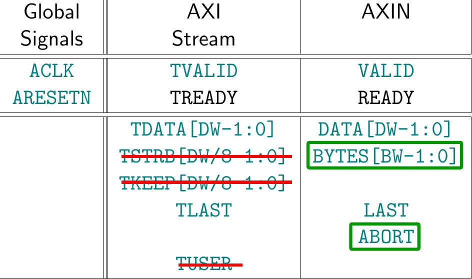 |
Let’s start with why the AXIN protocol is necessary. To put it in one word, AXIN is necessary because of backpressure. A true AXI stream implementation requires backpressure support–where a slave can tell the source it is not ready, and hold the ready line false indefinitely. However, in a network context the incoming network source has a limited buffer to support any backpressure. Hence the need for a new protocol.
Many have argued that this isn’t a sufficient need to justify creating a new protocol. Why not, they have argued, just buffer any incoming packets until a whole packet is in the buffer before forwarding it with full backpressure support? I’ve now seen several FIFO implementations which can do this sort of thing: buffer until a full packet has been received, then forward the packet via traditional AXI stream. The reason why I haven’t chosen this approach is because I had a customer ask for jumbo packet support (64kB+ packet sizes). True “jumbo packets” will be larger than my largest incoming FIFO, so I haven’t chosen this approach either.
The AXIN protocol differs
from AXI stream in two key respects.
The first is the addition of an ABORT signal. The ABORT signal can be
raised by an AXIN master
master at any time–even when VALID && !READY. If raised, it signals that
to the AXIN slave
that the current packet needs to be dropped in its entirety.
Many reasons might cause the ABORT to be asserted. For example, if the
initial packet source can’t handle the slave’s !READY signal, it could abort
the packet. If the packet CRC doesn’t match, the packet might also be aborted.
The second differences is the BYTES field. The original AXI stream
protocol
identified valid bytes via TKEEP and TSTRB. This allows packet data to
be discontinuous, and requires processing 2*WIDTH/8 signals per beat. The
AXIN protocol
instead uses a BYTES field having only $clog2(WIDTH/8) bits.
This BYTES field has the requirement that it must be zero (all bytes valid)
for all but the LAST beat, where it can be anything. This also carries
the implied requirement that all beats prior to the last beat must be full,
and the last beat must be right (or left) justified.
 |
When defining this protocol, I didn’t define whether or not it was little endian or big endian. As a consequence, some of the components of this design are little endian (Ethernet is little endian by nature), and others are big endian–since I implement both Wishbone and the ZipCPU in a big-endian fashion.
GTX PHY Front End
This design uses Xilinx’s GTX IO controllers to generate and ingest the 10Gb/s links. As I’ve configured them, the GTX IO controllers within this project act like 1:32 and 32:1 I/OSERDES macros, simplifying their implementation. Some key features of these components is that they can recover the clock when receiving and they can perform some amount of receive decision feedback channel equalization (DFE).
Although these transceivers appear amazing in capability, this great capability seems also to be their Achilles heel. I found myself reading, re-reading, and then re-reading their user guide again and again only to find myself confused regarding how to configure them. It didn’t help that many of the configuration options said that the Xilinx wizard’s configuration was to be used, and nothing more explained about the respective option. Nor did it help that many of the ports remain as legacy from previous versions of the controller, and the user guide suggests that they should not be used anymore. The GTX transceivers have many, many options associated with them, many of which are either not documented at all or are only poorly documented within the user guide. The “official” solution to this problem is to use a Vivado wizard for that purpose, and then to use one of the canned configurations Vivado offers. Perhaps this is ideal for Xilinx, who sells a fixed number of IP components based upon these configurations. However, this doesn’t really work well when you wish to post or share an all–RTL design. It also fails when you want to step off of the beaten path.
 |
As a result, I often ended up rather confused when configuring the GTX components.
The most obvious consequence of this is that I relied heavily on the GTX simulation models. This meant that I needed to model a 10Gb Ethernet link in Verilog to stimulate those models. If you look, you’ll notice I’ve got quite the clock recovery circuit written there in Verilog as well, so that I can recover the clock from the signal generated by the GTX simulation model. For those who know me, this is also a rather drastic departure from my all-Verilator approach to simulation. This is understandable, though, given both the complexity of these components and the fact that Xilinx did not provide a simulation model that would work with Verilator.
A second consequence is that I was never able to get the GTX’s 64/66b encoder/decoder working. I’m sure the interface was quite intuitive to whoever designed it. I just couldn’t get it working–not even in simulation. Then again, schedule pressure being what it was, it was just simpler to build (and formally verify) my own 32:66 and 66:32 gearboxes, and to use my own 66b synchronization module. Perhaps I might’ve figured out how to do this with their GTX transceiver if I had another month to work on it.
 |
Were I to offer any suggestions to Xilinx regarding their GTX design, I would simply suggest that they simplify it drastically. A good hardware IO module on an FPGA should handle any required high speed IO, while also leaving the protocol processing to be implemented in the FPGA fabric. It should also be versatile enough to continue to support the same protocols it currently supports (and more), without doing protocol specific handling, such as 64/66b or 8b/10b encoding and decoding, in the PHY components themselves. This means I’d probably remove phase alignment and “comma detection” from the PHY (I wasn’t using either of them for this project anyway) and force them back into the FPGA fabric. (Ask me again about these features, though, after I’ve had to use the GTX for a project that requires them.)
So, in the end, I used the GTX transceiver simply as a combined 32:1 OSERDES (for the transmit side) and a 1:32 ISERDES with clock recovery (for receive). Everything else was relegated to the fabric.
The Digital Front End
Ethernet processing in FPGA Logic was split into two parts. The first part, what I call the “digital front end”, converts the 32b data interface required by the PHY to the AXIN interfaces used by everything else. That’s all done in my netpath module.
Early on in this project, I diagrammed out this path, as shown in Fig. 7 below.
 |
The diagram begin as a simple block diagram of networking components that needed to be built and verified for the switch to work. (The color legend for this component is roughly the same as the color legend for the bus components shown in Fig. 2 above.)
Let’s walk through that module briefly here, working through first the receive chain followed by the transmit chain. In each case, processing is accomplished a discrete number of steps.
The (Incoming) RX Chain
The receive data processing chain starts with 32b words, sampled at 322MHz, and converts them to 128b wide AXIN packet streams sampled at 100MHz. (Why 100MHz? Because that was the DDR3 SDRAM memory controller’s speed in this design.)
-
As I mentioned in the GTX section above, I could never figure out how to get the 64/66b conversion working in the GTX front end. I’m sure Xilinx’s interface made sense to some, it just never quite made sense to me. As a result, it was just easier to use the PHY as a 32b ISERDES and process everything from there. This way I could control the signaling and gearbox handling. Even better, I could formally verify that I was doing things right using the signals I had that were under my own control.
That means that the first step is a 32:66b gearbox.
This gearbox is also where the 66b synchronization happens. For those not familiar with the 64/66b protocol, the extra two bits are used for synchronization. These two bits are guaranteed (by protocol) to be different. One bit combination will indicate the presence of packet data, the other indicates control information.
The alignment algorithm is fairly straightforward, and centers on an alignment counter. We first assume some arbitrary shift will produce aligned data. If the two control bits differ, this counter is incremented by one. Once the counter sets the MSB, this particular shift is declared to be aligned. If the two control bits are the same–that is if they are invalid, then the counter is decremented by three. Once the counter gets to zero, an alignment failure is declared and the algorithm moves on to check the next potential alignment by incrementing the shift amount.
From a rate standpoint, data comes in at 32b/clk, and leaves this gearbox via an AXI stream protocol that requires READY to be held high. There’s no room to support any backpressure here.
-
CDC from 322.3MHz to 200MHz
The problem with data coming in from the GTX PHY is that the received data is on a derived clock. As with any other externally provided clock, this means that the incoming clock (after recovery) will appear to be near its anticipated 10.3125GHz rate, but is highly unlikely to match any internal reference we have to 10.3125GHz exactly. Even when we divide it down by 32x, it will only be somewhere near a local 322.3MHz reference. For this reason, we want to cross from the per-channel clock rate to a common rate that can be used within our design–one allowing some timing overhead. In this case, we convert to a 200MHz clock.
The CDC is accomplished via a basic asynchronous FIFO, with the exception that the FIFO has been modified to recognize and propagate ABORT signals.
 |
-
Embedding clock and data together, as described above, requires having data that is sufficiently pseudorandom–otherwise there might not be enough bit transitions to reconstruct the clock signal. Likewise, if the incoming data isn’t sufficiently random, the 66b frame detector might suffer from “false locks” and fail to properly detect packet data. The 10Gb Ethernet specification describes a feedthrough scrambling algorithm that is to be applied to the 64 data bits of every 66b code word. Our first task, therefore, before we can process the 66b code word is to remove this scrambling.
-
Packet delimiter and fault detector
The next step is to convert these descrambled 66b codewords into our internal AXI network (AXIN) packet stream format.
For those familiar with Ethernet, they may recall that the Ethernet specification describes an XGMII “10Gigabit Media Independent Interface”, and suggests this interface should be used to feed the link. This project didn’t use the XGMII interface at all. Why not? Because the 66b encoding describes a set of either 64b data or 64b codewords. As a result, it makes sense to process these words 64b at a time–rather than the 32b at a time used by the XGMII protocol. Transitioning from 64b at a time to the 32b/clk of the XGMII protocol would require either processing data at the original 322.3MHz, or doing another clock domain crossing. It was just easier to go straight from the 66b format of the 10Gb interface directly to a 64b AXIN format.
Following this converter, we are now in a standard packet format. Everything from here until a (roughly) equivalent point in the transmit path takes place in this AXIN packet protocol.
While AXIN backpressure is supported from here on out, any backpressure will likely cause a dropped packet.
This is the first place in our processing chain where an ABORT may be generated. Any ABORTs that follow in the receive chain will either be propagated from this one, or due to subsequently detected errors in the packet stream.
-
Our next two steps massage our data just a little bit. This first step drops any packets shorter than the Ethernet minimum packet length: 64Bytes. These packets are dropped via the AXIN ABORT signal.
-
From here, we check packet CRCs. Any packet whose CRC doesn’t match will be dropped via an ABORT signal.
Although a basic CRC algorithm is quite straightforward, getting this algorithm to pass timing was a bit harder. Remember, packets arrive at 64b/clk, and can have any length. Therefore, the four byte CRC may be found on any byte boundary. That means we need to be prepared to check for any one of eight possible locations for a final CRC.
Our first attempt to check CRCs generated the correct CRC for each byte cut based upon the CRC from the last byte cut. This didn’t pass timing at 200MHz.
So, let’s take a moment to analyze the basic CRC algorithm. You can see it summarized in Verilog here. It works based upon a register I’ll call the “fill” (it’s called “current” in this Verilog summary). On each new bit, this “fill” is shifted right by one. The bit that then falls off the end of the register is exclusive OR’d with the incoming bit. If the result is a ‘1’, then a 32b value is added to the register, otherwise the result is left as a straight shift.
The important conclusion to draw from this is that the CRC “fill” register is simply propagated via linear algebra over GF2. It’s just a linear system! This is important to understand when working with any algorithm of this type.
Not only is this a linear system, but 1) the equations for each bit have fixed coefficients, and 2) they are roughly pseudorandom. That means that it should be possible to calculate any bit in the next CRC value based upon the previous fill and the new data using only 96 input bits, of which only a rough half of them will be non-zero (due to the pseudorandomness of the operator). Exclusive OR’ing 48bits together can be done with only 12 LUT6s and three levels of logic. (My out-of-date version of Yosys maps this to 20 LUT6s and 4 LUT4s.) My point is this: if you can convince your synthesis tool to remap this into a set of independnt linear equations, each will cheap and easy to implement.
Rewriting the CRC checker so that it first transformed the problem into a linear equation set, turned out to be just the juice needed to pass timing at 200MHz.
The result of this check module is that packets with failing CRCs will be ABORTed.
-
Resize from 64b/clk to 128b/clk
Since the system clock for this design is 100MHz, we need to cross clock domains one more time. This requires more parallelism, so we first increase our packet width from 64b/clk to 128b/clk in preparation of this final clock domain crossing.
The width converter used for this purpose has been designed to be very generic. As a result, you’ll find it used many times over in this design.
-
CDC from 200MHz to 100MHz – the bus clock speed
The last step of our incoming packet processor is to cross clock domains from our intermediate clock speed of 200MHz to 100MHz.
You may notice two additional blocks in Fig. 7 that aren’t connected to the data stream. These are outlined with a dashed line to indicate that they are optional. I placed the components in the chain because I have used a similar component in previous designs. These components might check the IP version, and potentially check that the header checksum or the packet length matches the one arriving. In other designs, these components would also verify that arriving packets were properly addressed to this destination. However, in this project, a choice was made early on that these IP-specific components wouldn’t be required for an Ethernet (not IP) switch, and so they have never been either built or integrated into the design.
From here on out, all processing takes place via the AXIN protocol. It is possible for a long packet to come through this portion of the interface, only to be ABORTed right at the end.
The (Outgoing) TX Chain
The other half of the digital front end takes packets incoming, via the AXIN protocol, and converts them to a set of 32b words for the GTX PHY. As with the receive processing chain, this is also accomplish in a series of discrete steps. Both halves are found within the netpath.v module.
-
CDC from 100MHz to 200MHz
Our first step is to cross from the 100MHz bus clock speed to a 200MHz intermediate clock speed. This simply moves us closer to the clock we ultimately need to be on, while reducing the amount of logic required on each step.
-
Resize from 128b/clk to 64b/clk
Our first step, once we cross back into the 200MHz clock domain, is to move from 128b/clk back to 64b/clk.
-
One problem with Ethernet transmission is that there’s no way to pause an outgoing packet. If the data isn’t ready when it’s time to send, the packet will need to be dropped. In order to keep this from happening, I’ve inserted what I call a “packet gate”. This component first loads incoming data into an AXIN FIFO, and then it holds up each individual packet until either 1) the entire packet has entered the FIFO, or 2) the FIFO becomes full. (Remember, backpressure is fully supported on the input.) This way we can have confidence, going forward, that any memory delays from the virtual FIFO feeding us our data from DDR3 memory will not cause us to drop packets. For shorter packets, this is a guarantee. For longer packets, the FIFO just mitigates any potential problems.
-
Spoiler
According to the Ethernet standard, I should have a packet spoiler at my next step. This spoiler would guarantee that any packets that must be ABORTed (for whatever reason) have failing CRCs.
This spoiler is not (yet) a part of my design. As a result, there is a (low) risk of a corrupt packet crossing the interface and (somehow) having a valid CRC on the other end.
-
At this point, it’s time to switch from the AXIN protocol back to the 66b/clk Ethernet network protocol. This includes inserting idle indications, link error (remote fault) indications, start and end of packet indications, as well as the packet data itself.
The big thing to remember here is that, once a packet enters this component, the packet data stream cannot be allowed to run dry without corrupting the outgoing data stream.
The result of this stage is a 66b AXI stream, whose VALID signal must be held high. READY will not be constantly high, but will be adjusted as necessary to match the speed of the ultimate transmit clock.
-
Just like the incoming packet data, we need to apply the same feedthrough scrambler to the data going out.
The result of this stage remains a 66b AXI stream. As with the prior stage, VALID needs to be held high.
-
As I mentioned earlier, the Xilinx GTX interface was a challenge to use and get working. I only use, therefore, the 32b interface as either a ISERDES or in this case an OSERDES type of operator. That means I need to move from 66b/clk to 32b/clk. The first half of this conversion takes place at the 200MHz clock rate, converting to 64b/clock.
-
CDC from 200MHz to 322.3MHz
From here, we can cross from our intermediate clock rate to the clock rate of the GTX transmitter. This is done via a standard asynchronous FIFO–such as we’ve written about on this blog before.
-
64/32b gearbox
The last step in the digital front end processor is to switch from 64b at a time to 32b at a time. Every other clock cycle reads a new 64b from the asynchronous FIFO and sends 32b of those 64b, whereas the other 32b are sent on the next clock.
Why not match the receive handler, and place the full 64/66b gearbox at the 322.3MHz rate? I tried. It didn’t pass timing. This two step approach, first going from 66b to 64b, and then from 64b to 32b is a compromise that works well enough.
That’s the two digital components of the PHY. Ever after these two components, everything takes place using the AXIN protocol.
The Switch
Now that we’ve moved to a common protocol, everything else can be handled via more generic components. This brings us to the core of the project, the 4x4 Ethernet switch function itself. This switch function is built in two parts. The first part is all about buffering incoming packets, and then routing them to their ultimate destinations. The second component, the routing algorithm, we’ll discuss in the next section.
The challenge of the switch is simply that packets may arrive at any time on any of our interfaces, and we want to make sure those packets can be properly routed to any outgoing interface–even if that outgoing interface is currently busy. While one approach might be to drop packets if the outgoing interface is busy, I chose the approach in this project of instead trying to buffer packets in memory via the virtual packet FIFOs.
-
Notify all routing tables of the incoming MAC
The first step in the switch is to grab the MAC source address from the incoming, and to notify all of the per-port routing tables of this MAC address.
We’ll discuss the routing algorithm more in the next section. It’s based upon first observing the Ethernet MAC addresses of where packets come from, and then routing packets to those ports when the addresses are known, or to all ports when the destination port is unknown.
-
The second step is to buffer the place the incoming packet into either a Virtual packet FIFO, or (based upon a configuration choice) just run it through a block RAM based NetFIFO.
-
Resize from 128b/clk to 512b/clk
Pushing all incoming packets into memory requires some attention be paid to memory bandwidth. At 128b/clk, there’s not enough bandwidth to push more than one incoming packet to memory, much less to read it back out again. For this reason, the DDR3 SDRAM width was selected to be wide enough to handle 512b/clock, or (equivalently) just over four incoming packets at once.
Sadly, that means we need to convert our packet width again. This time, we convert from 128b/clk to 512b/clk.
-
Incoming NetFIFO
SDRAM memory is not known for its predictable timing. Lots of things can happen that would make an incoming packet stream suffer. It could be that the CPU is currently using the memory and the network needs to wait. It might be that the memory is in the middle of a refresh cycle, and so all users need to wait. To make sure we can ride through any of these delays, the first step is to push the incoming packet into a block-RAM based AXIN FIFO.
-
Write packets to memory, then prefixing it with a 32b length word
Packet data is then written to memory.
My Virtual packet FIFO implementations work on a 32b alignment. This means that the incoming packet data may need to be realigned to avoid overwriting valid data that might already be in the FIFO.
Once the entire packet has been written to memory, the 32b word following is set to zero and the 32b word preceding the packet is then written with the packets’ size. This creates sort of a linked-list structure in memory, but one that only gets updated once a completed packet has been written to memory.
If the incoming packet is ever ABORTed, then the length word for the packet is kept at zero, and the next packet is just written to the place this one would’ve been written to.
Once the packet size word has been written to memory, and the memory has acknowledged it, the virtual packet FIFO writer then notifies the reader of its new write pointer. This signals to the reader that a new packet may be available.
-
Read packets back from memory, length word first
Once a packet has been written to memory, and hence once the write pointer changes, that packet can then be read from memory. This task works by first reading the packet length from memory, and then reading that many bytes from memory to form an outgoing packet.
One thing to beware of is that Wishbone has no ability to offer read backpressure on the bus. (AXI has the ability, but for performance and potential deadlock reasons it really shouldn’t be used.) This means that the part of the bus handler requesting data needs to be very aware of the number of words both requested by the bus as well as those contained in the synchronous FIFO to follow. Bus requests should not be issued unless room in the subsequent FIFO can be guaranteed.
I’ve also made an attempt to guarantee that FIFO performance will be handled on a burst basis. Hence, Wishbone requests will not be made unless the FIFO is less than half full, and they won’t stop being made until the FIFO is either fully committed, or the end of the packet has been reached.
-
This is just a basic synchronous FIFO with nothing special about it. It’s almost identical to the FIFO I’ve written about before, save that this one has been formally verified and gets used any time I need a FIFO.
-
Width adjustment, from 512b/clk back to 128b/clk
The last step in the virtual packet FIFO is to convert the bit width back from 512b/clk to 128b/clk.
Remember, 128b/clk is just barely enough to keep up at a 100MHz clock. We needed the 512b/clk width to use the memory. Now that we’re done with the memory transactions, we can go back to the 128b/clk rate to lower our design’s LUT count.
From this point forward, we can support as much backpressure as necessary. In many ways, this is the purpose of the virtual packet FIFOs: allowing us to buffer unlimited packet sizes in memory, so that we can guarantee full backpressure support following this point.
-
-
Get the packet’s destination MAC
Once a packet comes back out of the FIFO, the next step is to look up its MAC destination address. This can be found in the first 6 octets of the packet.
-
Look up a destination for this MAC
We then send this MAC address to the routing algorithm, to look up where it should be sent to.
-
Broadcast the packet to all desired destinations
The final step is to broadcast this packet to all of its potential destination ports at once.
This is built off of an AXIN broadcast component to create many AXIN streams from one, followed by an AXIN arbiter used to select from many sources to determine which source should be output at a given time.
That’s how most packets are handled. Packets to and from the CPU are handled differently. Unlike the regular packet paths, the CPU’s virtual FIFO involves the CPU. This changes the logic for this path subtly.
-
The CPUNet acts like its own port to the switch. That means that, internally, the switch is a 5x5 switch and not a 4x4 switch. It still has four physical ports, but it also has a virtual internal port going to the CPU.
-
The CPU port doesn’t require a virtual packet FIFO within the router core. Instead, its virtual packet FIFO is kept external to the router core.
-
As a result, packets come straight in to the switch component, get their MAC source recorded in the routing table, and then do all of the route processing other packets go through, save that they don’t need to through a virtual packet FIFO since they come from a virtual packet FIFO in the first place.
-
Likewise, in the reverse direction, packets routed to the CPU leave the router and go straight to the CPU’s virtual packet FIFO.
-
On entry, the CPU path has the option to filter out packets not addressed to its MAC–whatever assignment it is given.
-
However, for packet inspection and testing, this extra filter has often been turned off. Indeed, a special routing extension has been added to allow the CPU to “see” all ports coming in, and so it can inspect any packet going through the switch if bandwidth allows. (If bandwidth doesn’t allow this, packets in the switch may be dropped as well.)
The Routing Algorithm
The very first thing I built was the routing algorithm. This I felt was the core of the design, the soul and spirit of everything else. Without routing, there would be no switch.
The problem was simply that I’d never built a routing algorithm before.
My first and foremost goal, therefore, was to just build something that works. I judged that I could always come back later and build something better. Even better, because this system is open source, released under the Apache 2.0 license, someone else is always welcome to come back later and build something better. That’s how open source worked, right?
So let’s go through the basic requirements.
-
All packets must be routed.
-
Hence, if the router can’t tell which destination to send a packet to, then that packet should be broadcast to all destinations.
-
Packets should not be looped back upon their source.
-
Packets sent to broadcast addresses must be broadcast.
In hindsight, I should have built the table with some additional requirements:
-
It should be possible for the internal CPU to read the state of the table at any time.
-
The CPU should be able to generate configure fixed routes.
These include both routes where all packets from a given port go to a given destination port or set of ports, but also routes where a given MAC address goes to a given port.
-
In hindsight, my routing algorithm used a lot of internal logic resources. Perhaps a better solution might be to share the routing algorithm across ports. I didn’t do that. Instead, each port had its own routing table.
Given these requiremnts, I chose to build the routing algorithm around an internal routing table.
 |
Each network port was given its own routing table. As packets arrived,
the source MAC from the packet was isolated and then a doublet of source
[PORT, MAC] was forwarded to the routing tables in the design
associated with all of the other ports.
Each table entry has four components:
-
Each entry has a valid flag.
When a new source MAC doublet arrives, it will be placed into the first table entry without a valid entry within it. That entry will then become valid.
-
Each entry has a MAC address associated with it. This is the source address of the packet used to create this entry.
-
Each entry has a port number associated with it. This is the number of the port a packet with the given source address last arrived at.
-
Each entry has an age. (It’s really a timeout value …)
-
The age of any new entry to the table is given this timeout value. The timeout then counts down by one every clock cycle.
-
If a MAC declaration arrives for an existing entry, its timeout is reset. It will then start counting down from its full timeout value.
-
If 1) a new MAC declaration arrives for an entry that isn’t in the table, and , and 2) all entries are full, then 4) the oldest entry will be rewritten with this new entry.
Calculating “oldest” turned out to be one of the more difficult parts of this algorithm.
-
After a period of time, if no packets arrive from a particular source, then the entry will die of old age.
This allows us to accommodate routes that may need to change over time.
-
Note that no effort is made to sort this table one way or other.
Now that we have this table, we can look up the destination port for a given packet’s destination MAC address as follows:
-
If the packet’s destination MAC matches one from the table, the packet will then be sent sent to the port associated with that MAC.
This basically sends packets to the last source producing a packet with that MAC address. This will fail if a particular source sends to a particular destination, but that destination never responds.
Still, this constitutes a successful MAC table lookup.
-
If the destination MAC can’t be found in the table, then it will be forwarded to all possible destinations.
This constitutes a failed MAC lookup. In the worst case, this will increase network traffic going out by a factor of 4x in a 4x4 router.
This algorithm made a workable draft algorithm, up and until the network links needed to be debugged.
Just to make certain everything was working, the hardware was set up with the bench-top configuration shown in Fig. 10.
 |
-
Ports #0 and #1 were connected in a loopback fashion. Packets sent to port #0 would be received at port #1, and vice versa–packets sent to port #1 would be received at port #0.
-
Port #2 was connected to an external computer via a coaxial cable. We’ll call this PC#2.
-
Port #3 was connected to an external computer via an optical fiber. We’ll call this PC#3.
Now, let me ask, what’s that loopback going to do to our routing algorithm? Packets arriving on interface #2 for an unknown destination (PC#3’s address) will then be forwarded to interfaces #0 and #1 in addition to port #3. Ports #0 and #1 will then generate two incoming packets to be sent to the same unknown MAC address (PC#3’s address), which will then cause our table to learn that the MAC address generated by PC#2 comes from either port #0 or port #1. (A race condition will determine which port it gets registered to.) This is also going to flood our virtual FIFOs with a never ending number of packets.
This is not a good thing.
I tried a quick patch to solve this issue. The patch involved two new
parameters, OPT_ALWAYS and OPT_NEVER. Using these two options, I was
able to adjust the outgoing port so that it read:
	parameter	NETH=4;		// Number of ports
	parameter [NETH-1:0]	OPT_NEVER  = 4'h3;
	parameter [NETH-1:0]	OPT_ALWAYS = 4'h0;
	//
	// ...
	//

	TX_PORT <= (lkup_port & (~OPT_NEVER)) | OPT_ALWAYS;
I could then use this to keep my design from forwarding packets to port #0 or #1.
It wasn’t good enough.
For some reason, I was able to receive ARP requests from either ports #2 or #3, but they would never acknowledge any packets sent to them. So … I started instrumenting everything. I wondered if things were misrouted, so I tested sending packets everywhere arbitrarily. Suddenly, ports #2 and #3 started acknowledging pings! But when I cleaned up my arbitrary routing, they no longer acknowledged pings anymore.
This lead me into a cycle of adjusting OPT_NEVER and OPT_ALWAYS over
and over again, and rebuilding every time. Eventually, this got so painful
that I turned these into run-time configurable registers. (Lesson learned …)
I’ll admit, I started getting pretty frustrated over this one bug. The design worked in simulation. I could transmit packets from port #0 in simulation to port #3, going through the router, so I knew things should work–they just weren’t working. Like any good engineer, I started blaming the PCB designer for miswiring the board. To do that, though, I needed a good characterization of what was taking place on the board. So I started meticulously running tests and drawing things out. This lead to the following picture:
 |
This showed that packets sent to either ports #2 or #3 weren’t arriving. If I used the CPU to send to port #0, I could see the result on port #1. However, if I sent to port #1, nothing would be received on port #0. Just to make things really weird, if I sent to port #0 then ports #3 and #2 would see the packet, but I couldn’t send packets to ports #2 or #3.
Drawing the figure above out really helped. Perhaps you can even see the bug from the figure.
If not, here it was: I used one module to control all four GTX
transceivers.
This module had, as its input therefore, a value S_DATA containing 32-bits
for every port. This module was not subject to lint testing, however, since
… the GTX PHY couldn’t be Verilated–or I might’ve noticed what was going
on. I was then forwarding bits [63:0] of S_DATA to every outgoing port,
rather than 32-bits of zero followed by bits [32*gk +: 32] of S_DATA to
port gk. Because my network bench tests were limited to only look at
selected outputs, I then never noticed this issue. The result was that anything
sent to port #0 would be sent to all ports: #0-#3, and anything sent to
ports #1-#3 would go nowhere within the design.
So let me apologize now to the PCB designer for this board. This one was my bug after all.
Let me also suggest that this bug would’ve been much easier to find if I had designed the routing algorithm from the beginning so that I could test specific hardware paths. The CPU, for example, should be able to override any and all routing paths. Likewise, the CPU should be able to read (and so verify) any current routing paths.
A second problem with the router algorithm was that it consumed too many resources. The routing tables were first designed to have 64 entries in each of the four tables. When space got tight, this was dropped to 32 entries, and then to 16, and then down to 8. Any rewrite of this algorithm should therefore address the space used by the table–in addition to making it easier for the CPU to read and modify the table at will.
The Special Bus Arbiter
This design required a special Wishbone arbiter. To explain this need, though, I’ll need to do a little bit of math.
Suppose a port is receiving data at 10Gb/s. By the time we’ve adjusted the data down so that the stream is moving 512b per clock at a 10ns clock period, that means one 512b word will need to be written to memory 51.2ns.
 |
The typical DDR3 SDRAM access takes about 20 clock cycles of latency or so, with longer latency requirements if the SDRAM requires either a refresh cycle or a bank swapping cycle. Bank swapping can be avoided if the SDRAM accesses are burst together in a group–a good reason to use a FIFO, but there’s no easy way to avoid refresh cycles.
That’s only the first problem.
 |
The second problem is illustrated in Fig. 13 above. In this diagram, the
S1_* signals are from the first source, while the
S2_* signals are from the second source. The M_* signals would then go
to the downstream device–such as the DDR3 SDRAM or, in this case, a second
arbiter (shown above in Fig. 2) to then go to the DDR3 SDRAM. (Yeah, I know,
there’s a lot of levels to bus processing …)
The problem in this illustration is associated with how
Wishbone
normally works: CYC && STB are raised on the first beat of any transaction
from a given master, STB is dropped once all requests have been accepted,
and then CYC is dropped once all ACKs have been received. The arbiter
then takes a cycle to know that CYC has dropped, before allowing the
second master to have access to the bus. This creates a great inefficiency,
since the master isn’t likely to make any requests between when it drops STB
and when it drops CYC. Given what we know of DDR3 SDRAM, this inefficiency
could cost about 200ns per access.
However, if all four ports are receiving at the same time, then 512b will need to be written four times every 51ns, from each of four masters.
This requirement was impossible to meet with my normal
crossbar.
That crossbar
would wait until a master dropped CYC, before allowing a second
master to access the bus–suffering the inefficiency each time. This is all
illustrated in Fig. 13 above.
The solution that I’ve chosen to use is to create a special Wishbone master arbiter: one that multiplexes wishbone accesses together from multiple masters to a single slave. This way I could transition from one master’s bus requests to a second master’s bus requests, and then just route the return data to the next master looking for return data.
You can see how this might save time in Fig. 14 below.
 |
Notice how, in this figure, the requests get tightly packed together going to memory.
(Yes, this is what AXI was designed to do naturally, even though my AXI crossbars don’t yet do this.)
There are some consequences to this approach, however, that really keep
it from being used generally. One consequence is the loss of the ability
to lock the bus and do atomic transactions by simply holding CYC high.
(The virtual packet FIFOs don’t need atomic transactions, so this isn’t
an issue.)
A second consequence is in error handling. Because the
Wishbone bus aborts
any outstanding transactions on any error return, all outstanding requests
need to be aborted should any master receive a bus
error return. As a result, all
masters will report a bus error
return even if only one master caused the
error.
Given that the virtual packet FIFO bus masters would only ever interact with memory, this solution works in this circumstance. I may not be able to use it again.
Reusable Components
We’ve discussed hardware reuse on this blog before, and we’ll probably come back and do so again. I’ve said before, I will say again: well designed, well verified IP is gold in this business. It’s gold because it can be reused over and over again.
 |
As examples, the network portion of this project alone has reused many components, to include the ZipCPU, my asynchronous FIFO, my synchronous FIFO, my skidbuffer, and my Wishbone crossbar. If you look over the bus diagram in Fig. 2 above, you’ll also see many other components that may have either been reused, or are likely to be reused again–to include my Quad SPI flash controller, HDMI Controller(s), ICAPE2 controller, I2C Controller, and now my new SD-Card Controller–but I’m trying to limit today’s focus on the network specific components for now.
 |
Sadly, this is my fourth network design and many of the components from my first three network designs cannot be reused. My first network design used a 100M/s link. The next two network designs were based off of a 1Gb/s Ethernet, and so used either 8b/clk or 32b/clk–depending on which clock was being used. Any component specific to the bit-width of the network could (sadly) not be reused. Likewise, the first two of these three previous designs didn’t use the AXIN protocol–limiting their potential reuse.
 |
Perhaps this is to be expected. The first time you design a solution to a problem, you are likely to make a lot of mistakes. The second time you’ll get a lot closer. The third time even closer, etc. This is one of the reasons I like to tell students to “Plan for failure.” Why? Because “success” always comes after failure, and sometimes many “failures” are required to get there. Therefore, you need to start projects early enough that you have time to get past your early failures. Hence, you should always plan for these failures if you wish to succeed.
That said, this AXIN protocol was enough of a success on my third network project that I’m likely to use it again and again. The fact that I chose to use it here attests to the fact that it worked well enough on the last project that it didn’t need to be rebuilt at all.
That also means I’m likely going to be using and reusing many of the generic AXIN components from this project to the next. These include:
-
This is a basic FIFO, but for the AXIN protocol. Packets that have been completely received by the FIFO will not be aborted–no matter how the master adjusts the ABORT signal. What makes this component different from other network FIFOs I’ve seen is that the ABORT signal may still propagate from the input to the output prior to a full packet being recorded in the FIFO. This means that this particular network FIFO implementation is able to handle packet sizes that might be much larger than the FIFO itself.
Although my particular implementation doesn’t include the AXIN
BYTESsignal, the data width can be adjusted to include it alongside the data signal for no loss of functionality. -
This is a version of your basic skidbuffer, but this time applied to the AXIN protocol. As a result, it supports the ABORT signal, but in all other ways it’s just a basic skidbuffer.
This particular component was easy enough to design, and it would make a good classroom exercise for the student to design his own.
-
The most challenging component to verify, and hence to build, has been the virtual Packet FIFOs. On the other hand, these are very versatile, and so I’m likely to use them again and again in the future. This verification work, therefore, has been time well spent. You can read more about virtual packet FIFOs, what they are and how they work, in this article.
As of writing this, my virtual Packet FIFO. work isn’t quite done. There’s still a bit of a signaling issue, and the formal proof of the memory reader portion isn’t passing. However, the component is working in hardware so this is something I’ll just have to come back to as I have the opportunity.
Once completed, the only real upgrade potential remaining might be to convert these virutal FIFOs to AXI. Getting AXI bursting right won’t be easy, but it would certainly add value to my AXI library to have such a component within it.
-
The AXIN width converter will likely be reused. It should be generic enough to convert AXIN streams from any power of two byte width to any other. That means it will likely be reused on my next network project again as well. It’s just necessary network infrastructure, so that’s how it will be used and reused.
-
This component buffers either a whole packet, or fills its buffer with a full packet before releasing the packet downstream. It’s really nothing more than a network FIFO with some additional logic added. Still, this one is generic enough that it can be reused in other projects as necessary.
-
I’ve now written multiple components that can/will drop short packets. This new one, however, should be versatile enough to be able to be reused across projects.
-
As with the short packet detector, my CRC checker should work nicely across projects–even when the widths are different. This will then form the basis for future network CRC projects.
 |
-
The AXIN broadcasting component is only slightly modified from my AXI stream broadcaster. It’s a simple component: an AXIN stream comes in, specifying one (or more) destinations that this AXIN stream should be broadcast to. The broadcaster then sends a beat to each AXIN stream and, as beats are accepted from all outgoing streams, sends more beats.
Or, rather, that was the initial design.
As it turns out, this approach had a serious design flaw in it contributing to an honest to goodness, bona-fide deadlock. As a result, both this component, and the corresponding arbiter that follows it, needed fixing.
The new/updated algorithm includes two non-AXIN signals: CHREQ (channel request, from the master) and
ALLOC(channel allocated, returned from the slave). When “broadcasting” to a single port,CHREQwill equalVALID. When broadcasting to multiple ports, it will first set thisCHREQsignal to indicate each of the downstream ports it is attempting to broadcast to. This will be done before settingVALIDto forward any data downstream. The downstream ports, on seeing aCHREQsignal, will raise theALLOC(allocated channel) return signal if they aren’t busy. The design then waits forALLOCto matchCHREQ. Once the two match, the packet will be forwarded. If, however, after 64 clock cycles, enough channels haven’t been allocated to match the channel requests, then we may have detected a deadlock. In this case, all requests will be dropped for a pseudorandom time period beforeCHREQwill be raised to try again. -
As shown in Fig. 18 above, the AXIN arbiter is the other side of the AXIN broadcaster. Whereas the AXIN broadcaster takes a single AXIN stream input and (potentially) forwards it to multiple output streams, the arbiter takes multiple AXIN input streams and selects from among them to source a single output stream.
As with the broadcaster, the original design was quite simple: select from among many packet sources based upon the
VALIDsignal, and then hold on to that selection untilVALID && READY && LAST.The deadlock occurred when at least two simultaneous attempts were made to broadcast packets to two (or more) separate destinations, as shown in FIG:.
 |
If one destination arbitrated to allow the first source to transmit but the second destination chose to allow the second source, then the whole system would lock up and fail.
Now, the
arbiter
selects its incoming signal based upon CHREQ, and then
sets the ALLOC return signal once arbitration has been granted to let
the source know it has arbitration. Arbitration is then lost once CHREQ
is dropped–independent of whether a packet has (or has not) completed.
In this way, a failed arbitration (i.e. detected
deadlock)
can be dropped and try again before any packet information gets lost.
-
As long as there are multiple clocks in a design, there will be a need for crossing clock domains. This is uniquely true when there’s a difference a data input clock, data output, and memory clock domains.
Crossing clock domains with the AXIN protocol isn’t as pretty as when using the network FIFO. Indeed, there’s no easy way to ABORT and free the FIFO resources of a packet that’s been only partially accepted by an asynchronous FIFO. Instead, the ABORT signal is converted into a data wire and simply forwarded as normal through a standard asynchronous FIFO. It’s a simple enough approach, but it does nothing to free up FIFO resources on an ABORTed packet. However, freeing up FIFO resources can still be (mostly) accomplished by placing a small AXIN CDC (i.e. an asynchronous FIFO) back to back with the standard network FIFO. discussed above.
-
WBMArbiter (Wishbone master arbiter)
I mentioned this one in the last section. Although it’s not unique to networking, I may yet use this component again.
 |
There is another item worth mentioning in this list, and those are the two gearboxes. [1], [2]. I’m not listing these with the reusable components above, simply because I’m not likely to use these particular gearboxes outside of a 64/66b encoding system, so they aren’t really all that generic. However, the lessons learned from building them, together with the methodology for formally verifying them, is likely something I’ll remember long into the future when building gearboxes of other ratios.
Lessons Learned
Perhaps the biggest lesson (re)learned during this design is that you need to plan for debugging from the beginning. This includes some of the following lessons:
 |
-
Anytime a component generates an ABORT signal, that should be logged and counted somewhere. This is different from components propagating an ABORT signal.
-
Testing requires that the router have static paths, at least until the rest of the network interface works.
Port forwarding can also permit the CPU to inspect any packet crossing through the interface.
-
Bit-order in the ethernet specification is quite confusing.
I had to build and then rebuild the 66b to AXIN protocol component and its transmit counterpart many times over during this project–mostly because of misunderstandings of the Ethernet specification. This included confusions over how bytes are numbered within the 66b message word, the size of control bytes (7b) in 66b message words vs the size of data bytes (8b), whether the synchronization pattern was supposed to be
10for control words or01and so forth. As a result, even though I was able to get the design working with GTX transceivers in a 10Gb Ethernet test bench early on, I would later discover more than once that the “working” test bench and design didn’t match 10Gb Ethernet hardware components on the market.For example, the Ethernet specification indicates that the start of packet indication must include bits,
... 10101010 10101010followed by the octet10101011. What it doesn’t make clear is that these bits need to be read right to left. This meant that the final three bytes of any start of packet delimeter needed to be0x55,0x55, followed by0xd5rather than (as I first read the specification)0xaa,0xaa, followed by0xab. -
The routing algorithm above doesn’t work well in loopback situations.
As I mentioned above, this particular problem turned into a debugging nightmare. Even now that I have a working algorithm, I’m not yet convinced it does a good job handling this reality.
-
Look out for deadlocks!
Others who have dealt with deadlocks before have told me that 1) deadlocks are system architecture level problems, and 2) that they are easy enough to spot after you’ve had enough experience with them. In my case, I studied them back in my college days, but had never seen a deadlocks in real life before.
 |
- Because the routing tables were written entirely in RTL using Flip-Flops, and not using any block RAM, the CPU has no ability to read the tables back out to verify their functionality.
Finally, I’ve really enjoyed this network (AXIN) protocol. It’s met my needs now on multiple projects. Better yet, because I’ve made this protocol common across these projects, I can now re-use components between them.
Perhaps that should be a final lesson learned as well: well designed internal protocols facilitate design reuse.
Conclusion
So the big question I imagine on everybody’s mind at this point is, now that you have a 10Gb Ethernet switch, how well does it work?
Sadly, my answer to that (at present) is … I don’t know.
I’ve tested the design using scp to move files from one PC to another,
only to discover scp has internal speed limitations within it. This leaves
me and the project needing better test cases.
How about the hardware?
As with any PCB design, the original PCB design for this project has had some issues. The work presented above has been done with the original, first/draft board design. Part of my task has been to build enough RTL design to identify these issues. As of the this date, I’ve now worked over all of the hardware design save the SATA port. Yes, there are some issues that will need to be corrected in the next revision of the board. These issues, however, weren’t significant enough that they kept us from verifying the components on the board. As a result, I can now say with certainty that the 10GbE components of the board work–although, IIRC, we were going to change the polarity of some of the LED controls associated with it. Still, its enough to say it works.
The flash, SD card, and eMMC interfaces? Those will need some redesign work, and so they should be fixed on the next revision of the board. As for the 10GbE interfaces? Those work.
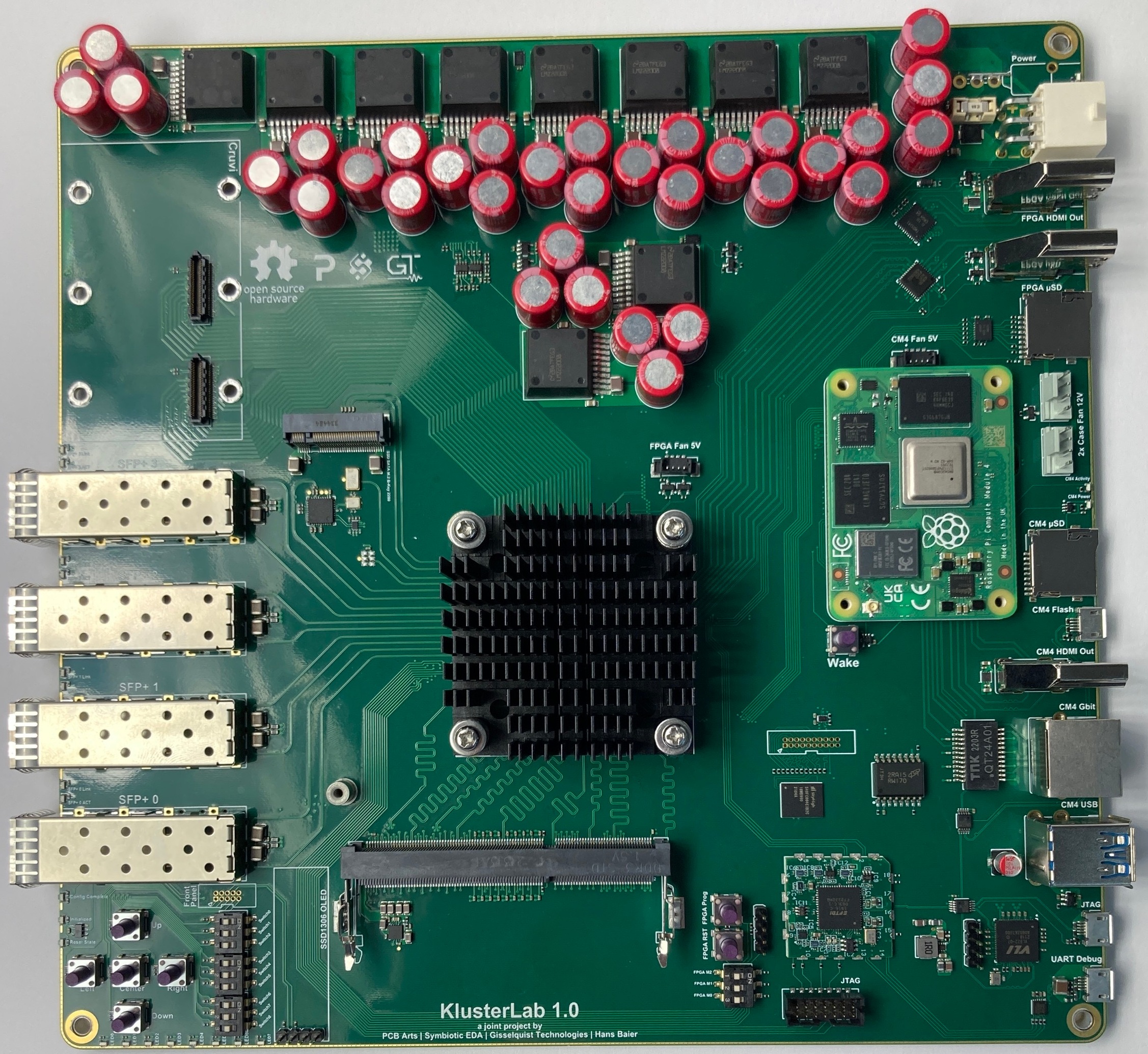
If you are interested in one of these boards to work with, then please contact Edmund, at Symbiotic EDA, for details.
If the Lord wills, there are several components of this design that might be fun to blog about. These include the formal property set that I’ve been using to verify AXIN components, the AXIN Skidbuffer or even the NetFIFO.
For now, I’ll just note that the design is posted on github, licensed under Apache 2.0, and I will invite others to examine it and make comments on it.
This also cometh from the LORD of Hosts, which is wonderful in counsel, and excellent in working. (Is 28:29)