
Building a Simple Logic PLL
There’s one signal processing component that has always felt like a black art to me, and that is a Phase Locked Loop or PLL. If you aren’t familiar with PLLs, a PLL is a closed loop control system designed to match an incoming sine wave with a reconstructed sine wave that tracks both the phase and (optionally) the frequency of an incoming sine wave.
PLLs are important parts of many Digital Signal Processing (DSP) systems, including (but not limited to):
-
Recovering the implicit (or explicit) clock from an incoming signal. Inside digital logic, clock recovery becomes very important when you are trying to transfer data between two components. Even components that have two independent clocks, each supposedly tuned to “the same” clock frequency, will likely have their clocks wander in phase with respect to each other.
You may be familiar with the hard PLL components on your board which are used to do this exact thing.
-
New clock signal generation. For example, a PLL can often be used to create a clock
Ntimes faster or slower than an incoming reference clock. -
In a commercial broadcast FM signal, a PLL is often used to undo the FM modulation. This may also include a separate PLL component used to lock onto the stereo component of the signal–and even to determine if it is present.
-
Of course, my favorite use for a PLL is to lock onto the baud rate and carrier phase of a digital communications waveform. The baud clock recovery portion of this circuit in the receiver is used to determine the sampling point (the middle) of any received bits.
My own first experience with PLLs came as part of an “Everything you need to know about DSP” type of course offered at my workplace. In this course, the instructor presented two very simple PLL structures that have served me well ever since.
If the Lord permits, I may have the opportunity to share some of these same fundamental PLL structures here with you here on this blog. I’ll try to keep them as simple as I can. For example, the PLL I’ll present below has only about 84 lines of logic to its implementation. Sound simple enough?
Since that first class, though, I decided that I didn’t know enough about this black art, and that I wanted to learn more about PLLs. After a bit of browsing on Amazon, I came across Floyd M. Gardner’s book, Phaselock Techniques. One particular comment in his introductory chapter caught my eye, and I’d like to repeat it for you here:
Every PLL is nonlinear. Tools for analysis of nonlinear systems are exceedingly cumbersome and provide meager benefits compared to the powerful analytical tools available for linear systems. Fortunately, most (but not all) PLLs of interest can be analyzed by linear techniques when in their locked condition. This book argues throughout that linear methods are sufficient for the bulk of the analysis and initial design of most PLLs. Therefore, linear approximations are employed wherever feasible.
I was instantly sold! I’ve not regretted this purchase since then, for Mr. Gardner was true to his word and I have learned much from his book. That said, I’ve never taken any academic classes studying PLL design or analysis, so I can’t really comment on whether or not other books are better or worse than Gardner’s.
So today let’s talk about how to build a really simple
PLL. I’m going to call
this a logic PLL
for the simple reason that it will take as an input a logical
(boolean)
clock signal (0 or 1). Internally, the
logic PLL
will use only simple boolean
logic–there will be no N-bit samples or even
any sine wave
generation
within the logic below. Indeed, you might need to look carefully if you want
to find the multiplies.
Components of a PLL
The basic form of a PLL is that of a control loop. The input to this loop is a sine wave.
 |
Outputs can be taken from any number of locations, depending upon the purpose of the PLL.
The loop begins with an incoming sine wave that is passed into a phase detector. The phase detector is used to compare the phase of the incoming sine wave against a reconstructed sine wave produced internally. The output of this phase detector is an error signal. This error signal is then optionally filtered, and fed into two portions of the circuit: one to track frequency and the other to track phase. These two portions combine within a Numerically Controlled Oscillator (NCO) to create a new phase for the reconstructed sine wave. That phase is then used as an input to a sine wave generator to create a reconstructed sine wave, which is then used as the second input to the phase detector and the loop repeats.
The PLL presented below will contain all of these basic components, with the exception that the incoming sine wave will be represented by a 1-bit clock signal, and the reconstructed sine wave will have only a 1-bit amplitude. Put together, these two changes will allow us to keep the logic count of this “logic PLL” quite low. Since low logic count often correlates with high FPGA speed, these two changes should allow this PLL to run at a high internal speed within an FPGA.
A Basic PLL interface
 |
A typical PLL component might have a component I/O diagram like the one in Fig 2 to the right. Indeed, today’s logic PLL will implement most of this interface–with the exception of the lock indicator output.
The basic signals are:
-
An incoming clock signal,
i_clk. While not shown in Fig 2, today’s logic is going to be synchronous, and hence everything will take place on clock edges. -
A means of setting the frequency of the internal NCO component. In this case, any time the load new frequency flag is true, we’ll call this
i_ldbelow, the internal phase increment of the NCO will be forced to the frequency control value,i_step. Whilei_ldis high, the logic PLL will not track any frequency changes. -
The bandwidth of this control loop will be set via the loop bandwidth control input,
i_lgcoeffwhich I may reference asLGCOEFFbelow, so that the internal loop gain is set to2^(-LGCOEFF). This will control how fast the loop locks on to an incoming clock signal. -
This leaves the incoming sine wave,
i_input. We’ll assume this is either on or off, much like any logical clock signal. We’ll also use the “global CE” strategy, captured by the clock enable (CE) line, referenced below asi_ce. Under this strategy, bothi_inputand the outputso_phaseando_errwill need to be valid any timei_ceis true, and should only change at that time.From a timing standpoint, we’ll want to be able to handle the case where
i_ceis held at one, so as to make this a high speed PLL implementation.
There are two basic outputs of this PLL:
-
The error signal coming out of the phase detector.
Changes in this phase error signal, since they will be proportional to frequency, are often used within an FM demodulator.
You could also use this error signal to create a locked indication if you wanted.
-
We’ll also produce the basic phase of the internal oscillator,
o_phase. This signal is the same as the phase counter we used in our NCO discussion.Because this phase tracks the incoming signal, it can also be used as an indication of when to sample an incoming data bit.
Further, since we’ll be matching the most-significant bit of this phase value to the incoming clock signal, this also creates a stable clock output.
Put together, you can see the prototype for our logic PLL written out in Verilog below.
module	sdpll(i_clk, i_ld, i_step, i_ce, i_input, i_lgcoeff, o_phase, o_err);
	parameter		PHASE_BITS = 32;
	parameter	[0:0]	OPT_TRACK_FREQUENCY = 1'b1;
	localparam		MSB=PHASE_BITS-1;
	//
	input	wire	i_clk;
	//
	input	wire			i_ld;
	input	wire	[(MSB-1):0]	i_step;
	//
	input	wire			i_ce;
	input	wire			i_input;
	input	wire	[4:0]		i_lgcoeff;
	output	wire	[PHASE_BITS-1:0] o_phase;
	output	reg	[1:0]		o_err;
	//
One item to note is that
this PLL design can
be set to optionally track
frequency, as well as
phase,
by just setting the OPT_TRACK_FREQUENCY flag above.
As discussed above, the goal of
this PLL
is to track the incoming signal, i_input, and to produce a reconstructed clock
signal. This reconstructed clock signal will be captured by the most
significant bit of the output, o_phase.
Further, while we are not creating a lock signal today, we could easily
create one later by using the o_err signal if we wanted to. Indeed, such
a lock signal isn’t really all that hard to create: just pass the
(o_err == 2'b00) signal into a recursive
average.
Once the output of such a recursive
average
falls below a threshold, the loop may be assumed to be locked.
These, though, are the basic components of any PLL, and specifically the components we will implement as part of our module today.
The Logic Based NCO
We discussed how to build an NCO in an earlier article. Today, we are going to use nearly the same logic to create a clock signal, and we’ll then approximate the sine wave generator with the most significant bit of the NCO’s phase accumulator.
This is also the same logic used by the fractional counter timing approach we discussed earlier. As you may recall from that discussion, a clock of an arbitrary frequency may be generated by just examining the most significant bit of a counter.
That means we’ll be starting with logic that looks like the following.
	initial	ctr = 0;
	always @(posedge i_clk)
		if (i_ce)
			ctr <= ctr + r_step;
In this case, the frequency of the
clock generated by this counter will be given by the product of the counter’s
phase step (divided by
2^(PHASE_BITS)) times the overall clock rate.
 |
Feel free to reference the NCO article if any of this doesn’t look familiar to you here.
Setting the frequency of this
phase accumulator
(really a phase
step) is as simple as setting the r_step value any time the user
wishes to adjust the frequency
of the basic NCO,
	always @(posedge i_clk)
		if (i_ld)
			r_step <= { 1'b0, i_step };
This is just our starting point, however, as both of these blocks will need some adjustment if we wish to track the phase and (optionally) the frequency of an incoming sine wave.
As we work through the logic of
this
PLL,
you’ll find this
phase
accumulator value,
ctr, comes back again and again.
A Logic Phase Detector
The goal of the phase detector is to create a signal that is proportional to how far the PLL needs to be made faster or slowed down. Traditionally, a phase detector is created by taking a product of the input (co)sine wave with a reconstructed sine wave separated by ninety degrees. The resulting phase error signal is then proportional to how far the phase accumulator is from the incoming signal.
This is not going to be our chosen approach today. Instead, we’ll use an ad-hoc approach–one that generates a two-bit phase error signal indicating not only the presence of an error but also the direction the internal counter needs to be adjusted. This will not be proportional, since we are only going to capture a two bit phase error signal, but rather somewhat nonlinear–perfect, though, for a boolean logic implementation.
 |
Let’s consider how this phase detector needs to work. If the regenerated clock changes before the incoming clock, as shown in Fig 3, then we’ll say that this regenerated clock leads the input. Such a leading situation will create a negative phase error, indicating that we will want to slow down our PLL. Further, any time the two signals, both the incoming clock and the regenerated one, are identical we’ll design our phase detector to indicate zero phase error.
 |
On the other hand, if the regenerated clock changes after the incoming clock, such as is shown in Fig 4, then our reconstructed clock isn’t transitioning fast enough. We’ll say in this case that the regenerated clock lags the input. To correct this, we’ll want to speed up our internal clock to “catch up” to the incoming clock, hence we want to create a positive phase error in this case. As before, though, any time the two signals agree we’ll want to keep the phase error at zero.
But how shall we tell whether we are leading or lagging?
We’ll start by keeping track of the input sign from the last time the input and reconstructed signal agree.
	initial	agreed_output = 0;
	always @(posedge i_clk)
	if (i_ce)
	begin
		if ((i_input)&&(ctr[MSB]))
			agreed_output <= 1'b1;
		else if ((!i_input)&&(!ctr[MSB]))
			agreed_output <= 1'b0;
	end
Whether or not we are leading the incoming clock, can then be determined with respsct to this last agreed upon output.
	always @(*)
		if (agreed_output)
			// We were last high.  Lead is true now
			// if the counter goes low before the input
			lead = (!ctr[MSB])&&(i_input);
		else
			// The last time we agreed, both the counter
			// and the input were low.   This will be
			// true if the counter goes high before the input
			lead = (ctr[MSB])&&(!i_input);
Since the above logic didn’t capture whether or not the current regenerated
bit, ctr[MSB] matched the i_input, we’ll capture that in an internal
phase_err exists signal.
	// Any disagreement between the high order counter bit and the input
	// is a phase error that we will need to correct
	assign	phase_err = (ctr[MSB] != i_input);
We can put these two values together, phase_err and lead, to create a
2-bit output error value, representing either -1, 0, or 1.
	initial	o_err = 2'h0;
	always @(posedge i_clk)
	if (i_ce)
		o_err <= (!phase_err) ? 2'b00 : ((lead) ? 2'b11 : 2'b01);
We won’t actually use this value internally, but rather the phase_err and
lead signals. However, the o_err signal should make it easier to understand
the phase_err and lead signals.
A Logic PLL: Type 1
A “Type 1”
PLL
is one that tracks phase,
but not frequency. This portion of a
PLL
accepts as an input the
phase
error, (optionally) filters
it, and then corrects the internal
phase accumulator,
ctr, based upon the result. In general, this involves applying some sort
of linear operator to the
phase
error signal, and then adding the result of that operator to the
phase accumulator.
 |
Today’s
logic PLL
is no different. In this case, though, we’ll skip the optional
lowpass filter
and just multiply our incoming
phase
error by a constant before adding it to our
phase accumulator.
Even better, because the incoming error was either -1, 0, or 1, no real
multiplication is required–we can use a nested if instead.
As for the constant, what constant shall we use? As we suggested above, we’ll
use the absolutely simplest constant we can pick: 2^(-LGCOEFF).
	initial	phase_correction = 0;
	always @(posedge i_clk)
		phase_correction <= {1'b1,{(MSB){1'b0}}} >> i_lgcoeff;
We’ll show some charts later on illustrating how this coefficient changes
things. In general, the larger 2^(-LGCOEFF) is,
the faster the loop will track any changes. At the same time, larger values of
2^(-LGCOEFF) will also cause the
PLL
to pass any jitters in the incoming clock directly into the reconstructed
signal.
Now with this information, we can adjust our
phase
value, ctr, using what we now know.
First, if there is no
phase
error, then all we need to do is to continue to step our
phase
forward at the frequency rate
set by r_step.
	initial	ctr = 0;
	always @(posedge i_clk)
		if (i_ce)
		begin
			// ...
			if (!phase_err)
				ctr <= ctr + r_step;
Otherwise, if phase_err != 0, then the incoming and regenerated clocks didn’t
match. In this case we’ll need to bump our counter a little more forward than
just a normal
frequency
step, or slow it down by a little less than the normal
frequency
step. The difference between these two is going to be
based upon whether or not the lead flag is true–as we discussed above.
			else if (lead)
				ctr <= ctr + r_step - phase_correction;
			// ...
			else
				ctr <= ctr + r_step + phase_correction;
		end
As a final step, we’ll place this counter on the output for examination and/or re-use as desired.
assign o_phase = ctr;That’s all there is to the
phase
correction step! There’s no more black magic to it than the logic above.
Indeed, if you wanted to we could stop here and have a fully functional
PLL.
If the frequency
step, r_step,
of that PLL
was close enough to the right value, then nothing more would need to be
done–this PLL would track
the phase
an incoming 1-bit clock signal.
On the other hand, if you need (or want) to discover what frequency step to use (within reason, from a good initial guess), then you’ll want to add the type-2 PLL logic in the next section to the logic we just discussed above.
A Logic PLL: Type 2
In many cases when using a
PLL,
you will want to track both the
frequency
of the incoming signal as well as its
phase.
As we discussed in our
NCO
article,
frequency
is represented as a regular change of
phase.
You may have noticed how we kept track of this above in r_step. If you want
to track
frequency
as well as
phase,
then you’ll want to adjust this r_step value based upon the
phase
error as well. Such a
PLL
that tracks
frequency
as well as
phase
is called a type-2
PLL.
The basic means of extending the type-1
PLL
into a type-2
PLL
is to multiply the
(optionally) filtered
phase
error by a constant and then adjust the
phase
step due to frequency, i.e.
the frequency
r_step, by that amount. This basic logic is shown below in addition
to the type-1 logic we developed above.
 |
Up until this point, there hasn’t been much black magic. We’ve just pushed
a counter forward or backwards by some nominal amount based upon the sign of
a measured phase
error. Here, though, I’m going to introduce the
frequency
adjustment coefficient, 1/4 2^(-2LGCOEFF), that I’m not going to derive
today. This particular coefficient is designed to make sure this
PLL
is critically damped.
Practically, this just means that this
PLL
will converge faster than any other
PLL
having a phase
correction coefficient of 2^(-LGCOEFF).
That’s a good thing.
Hence, our frequency correction constant is given by,
	initial	freq_correction = 0;
	always @(posedge i_clk)
		freq_correction <= { 3'b001, {(MSB-2){1'b0}} } >> (2*i_lgcoeff);
So, how shall we update our step? First, we’ll allow this number to be loaded–so that you can set what frequency you expect this PLL to converge around.
	always @(posedge i_clk)
		if (i_ld)
			r_step <= { 1'b0, i_step };
Likewise, we’ll use the parameter,
OPT_TRACK_FREQUENCY, to control whether or not
frequency
tracking is enabled.
		else if ((OPT_TRACK_FREQUENCY)&&(phase_err))
		begin
Beyond that, any time we need to slow down, we’ll subtract this frequency correction value and any time we need to speed up we’ll add this frequency correction value.
			if (lead)
				r_step <= r_step - freq_correction;
			else
				r_step <= r_step + freq_correction;
		end
You can find all of this code in the sdpll.v file within my new repository holding demonstration PLL implementations.
Performance
Shall we see how well this PLL performs?
You can find a
Verilator
based
test bench
here, called sdpll_tb.cpp.
This test bench
code
primarily
works by starting with a set of initial conditions and then running the
PLL
to see what happens. Unlike most of my test benches, there’s no SUCCESS
output at the end of
this test bench
to indicate that it worked. Instead, the
test bench
will print Simulation complete to indicate that it
to completion–you’ll still need to check the results produced by the
simulation
to know if it worked.
For our purpose today, I’ve chosen to use a random phase. for our initial condition, together with a frequency that’s about five system clocks per input clock. Where the test setup gets interesting is the fact that we’ll start by loading the PLL with a frequency that’s too fast by about 12%.
	tb.i_lgcoeff = 6;
	lclphase     = rand();
	lclstep      = 0x31415928;
	tb.i_step    = lclstep + (lclstep>>3); // Too fast
	tb.i_ld      = 1;
	tb.i_clk     = 0;
	tb.i_ce      = 1;
Then, within the Verilator per-clock loop,
	for(int k=0; k<65536*32; k++) {
		tb.eval();
		tfp->dump(10*k+8);
		tb.i_clk = 1;
		tb.eval();
		tfp->dump(10*k+10);
		tb.i_clk = 0;
		tb.eval();
		tfp->dump(10*k+15);
we’ll record several performance numbers.
		{
			int	od[6];
			od[0] = lclphase;
			od[1] = tb.v__DOT__r_step;
			od[2] = tb.i_input;
			od[3] = tb.o_err;
			if (od[3] == 3)
				od[3] = -1;
			od[4] = tb.v__DOT__ctr;
			od[5] = tb.v__DOT__ctr - lclphase;
			od[6] = tb.o_dbg << (32-10);
			od[6]>>= (32-10);

			fwrite(od, sizeof(int), 7, intfp);
These are …
-
The local simulation sine wave phase that’s driving the test,
lclphase. -
The incoming input signal to the PLL,
i_input -
The error signal,
o_err, created by the PLL, and interpreted here as a signed value -
The internal PLL counter,
ctr -
The difference between the internal PLL counter,
ctrand the simulation phase,lclphase, truncated to the number of phase error bits (32) -
Finally, a filtered error output signal,
o_dbg. This signal isn’t really part of our PLL implementation, but since I already had the filter lying around from a previous post it made sense to re-use it here.
At the end of the loop, and so once per clock, we’ll update our
simulation
phase accumulator,
lclphase, and create the next input for the
PLL
to act upon.
		tb.i_ld = 0;
		tb.i_clk = 0;
		lclphase += lclstep;
		tb.i_input = (lclphase >> 31)&1;
Now that we have this PLL instrumented, we can answer the question of, how well does this PLL work?
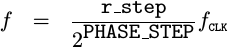
While we could look at the error output of the PLL, as shown in Fig 7,
 |
the result isn’t really all that meaningful.
Sadly, because the error is a discretized signal of -1, 0, or 1, it’s rather difficult to get a good feel for what is going on. Clearly there’s more error on the left side, but by how much?
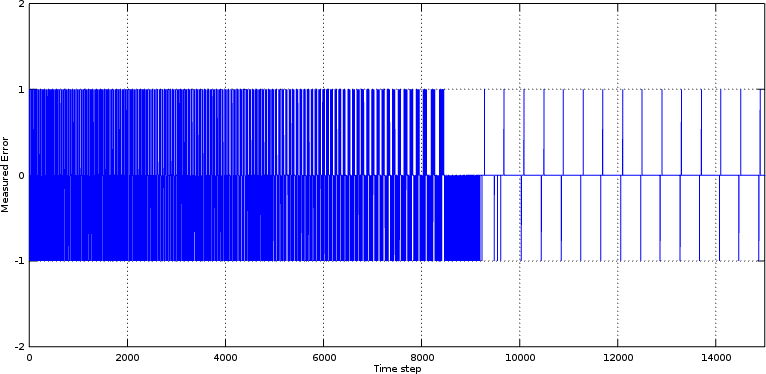
So, instead, let’s compare the difference between the
simulation’s
internal lclphase variable and the
reconstructed
ctr value. This is shown in Fig 8 as the actual phase error.
 |
This is more revealing. Here we can see that the phase difference on the left side of the chart is wandering all over the place. Why? Because the PLL has yet to lock. Eventually, it comes to a locked position and then the error settles out into a steady state.
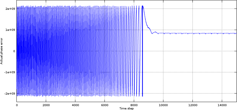
Where this gets fascinating, though, is if you evaluate the
phase
error of
the PLL
across multiple coefficient choices. We’ll try
i_lgcoeff ranging from 4 to 6, and plot the results in Fig 9.
 |
There’s a couple of things to notice in Fig 9. First, the larger the
coefficient (i.e. the smaller i_lgcoeff), the faster
the PLL
converges. However,
the PLL
doesn’t settle as nicely when i_lgcoeff is 4 compared to how it settles
when i_lgcoeff is 6. On the other hand, even though the smaller
values of 2^(-i_lgcoeff) take longer to converge, once they do converge
the remaining residual error is much smaller.
We can also return to the PLL’s phase error output and average it using a 3839 point boxcar filter. (There is no particular significance to this number, 3839. Feel free to try other amounts if you would like.) This will help to accumulate the errors long enough to draw a conclusion from them. You can see this result in Fig 10.
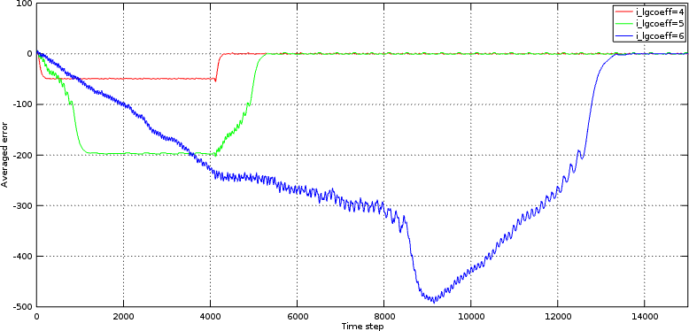 |
The first conclusion to draw from Fig 10 is that we
averaged
too many sample points together for i_lgcoeff=4 and i_lgcoeff=5. This is
seen by the fact that the filtered error signals appear like negative rectangle
functions. In spite of this artifact, you can see that the
i_lgcoeff=6 trace accumulates a much larger error before it finally locks.
Further, when each of these traces gets to the locked condition, they suddenly
go to zero. Finally, as before with the residual error, the i_lgcoeff=6 ends
up with smaller residual error. (This is harder to see on the chart.)
The last variable to consider is the
frequency
step size. Remember, we started
this PLL
with a frequency
value that was about 12% too fast. Hence, the step size
needs to come down a bit. In Fig 11, you can see the step size, r_step,
coming down for all three traces until the respective
PLL’s
lock. Once lock has been achieved, the traces appear to flatten out.
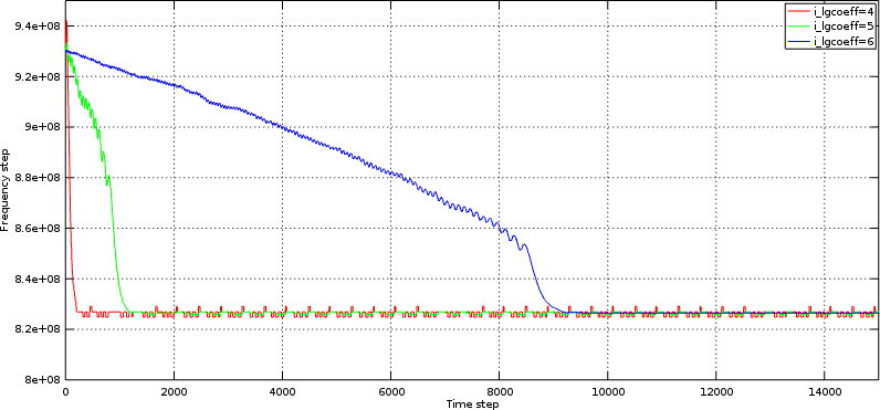 |
However, as before, the i_lgcoeff=4 trace has the most noise on it following
convergence, whereas the i_lgcoeff=6 trace has less noise.
Together, these charts should be sufficient to not only demonstrate that this PLL implementation “works”, but also to give you an indication as to how well it works.
Conclusion
Building a PLL doesn’t need to be the black art I once thought it was. All of the parts and pieces have fairly simple definitions, and the implementation of this simple PLL really wasn’t all that complex. Even better, since I’ve posted this code on GitHub, you are welcome to try it out yourself to see how well (or poorly) it works for your problem set.
Of course, I haven’t exhausted the topic of either PLL design or analysis–I’ve just presented a single PLL implementation that has worked well for me over many years. As examples of some of the things we haven’t discussed:
-
There’s a real reason and theory behind why we chose the frequency correction value we did. Perhaps if someone is interested, I could go through this theory. Be prepared, though, it depends upon a solid understanding of Z transforms.
-
You may also remember that I skipped the phase error filters in this implementation. While a simple recursive average filter works nicely, the recursive average coefficient couples with the phase and frequency correction coefficients of the PLL, necessitating a change to how these coefficients need to be calculated should you go this route.
-
The actual study and analysis of PLLs includes a study of how to predict many of the charts I presented above in Figures 7-11. While it’s a valuable study that I would commend to anyone interested, it’s not required to understand any of the figures.
Further, I know I said that PLLs could be used for clock recovery. While today’s logic PLL implements a valuable circuit that can handle that task, you may find that the hardware implemented PLLs within your FPGA are much more appropriate for this purpose than the PLL we designed today.
Finally, this isn’t the last word on FPGA PLL implementation. Other PLL implementations are also valuable, such as the more traditional (non-binary) PLL implementations, or even logic PLLs designed to run at many samples per clock. These will need to remain a topic for future posts.
But the men marvelled, saying, What manner of man is this, that even the winds and the sea obey him! (Matt 8:24)