
Debugging video from across the ocean
I’ve come across two approaches to video synchronization. The first, used by a lot of the Xilinx IP I’ve come across, is to hold the video pipeline in reset until everything is ready and then release the resets (in the right and proper order) to get the design started. If something goes wrong, however, there’s no room for recovery. The second approach is the approach I like to use, which is to build video components that are inherently “stable”: 1) if they ever lose synchronization, they will naturally work their way back into synchronization, and 2) once synchronized they will not get out of sync.
At least that’s the goal. It’s a great goal, too–when it works.
Today’s story is about what happens when a “robust” video display isn’t.
System Overview
Let’s start at the top level: I’m working on building a SONAR device.
This device will be placed in the water, and it will sample acoustic data. All of the electronics will be contained within a pressure chamber, with the only interface to the outside world being a single cable providing both Ethernet and power.
Here’s the picture I used to capture this idea when we discussed the network protocols that would be required to debug this device.
 |
This “wet” device will then connect to a “dry” device (kept on land, via Ethernet) where the sampled data can then be read, stored and processed.
Now into today’s detail: while my customer has provided no requirement for real-time processing, there’s arguably a need for it during development testing. Even if there’s no need for real-time processing in the final delivery, there’s arguably a need for it in the lab leading up to that final delivery. That is, I’d like to be able to just glance at my lab setup and know (at a glance or two) that things are working. For this reason, I’d like some real time displays that I can read, at a glance, and know that things are working.
So, what do we have available to us to get us closer?
Display Architecture
Some time ago, I built several RTL “display” modules to use for this lab-testing purpose. In general, these modules take an AXI stream of incoming data, and they produce an AXI video stream for display. At present, there are only five of these graphics display modules:
-
Histograms are exceptionally useful for diagnosing any A/D collection issues, so having a live histogram display to provide insight into the sampled data distribution just makes sense.
However, histogram displays need a tremendous dynamic range. How do you handle that in hardware? Yeah, that was part of the challenge when building this display. It involved figuring out how to build multiplies and divides without doing either multiplication or division. A fun project, though.
-
By “trace”, I mean something to show the time series, such as a plot of voltage against time. My big challenge with this display so far has been the reality that the SONAR A/D chips can produce more data than they eye can quickly process.
Now that we’ve been through a test or two with the hardware, I have a better idea of what would be valuable here. As a result, I’m likely going to take the absolute value of voltages across a significant fraction of a second, and then use that approach to display a couple of seconds worth of data on the screen. Thankfully, my trace display module is quite flexible, and should be able to display anything you give to it by way of an AXI Stream input.
-
The very first time my wife came to a family day at the office, way back in the 1995-96 time frame or so, the office had a display set up with a microphone and a sliding spectral raster. I was in awe! You could speak, and see what your voice “looked” like spectrally over time. You could hit the table, whistle, bark, whatever, and every sound you made would look different.
I’ve since built this kind of capability many times over, and even studied the best ways to do it from a mathematical standpoint.
In the SONAR world, you’ll find this sort of thing really helps you visualize what’s going on in your data streams–what sounds are your sensors picking up, what frequencies are they at, etc. A good raster will let you “see” motors in the water–all very valuable.
-
A spectrogram, via the same trace module
This primarily involves plotting the absolute values of the data coming out of an FFT, applied to the incoming data. Thankfully, the trace module is robust enough to handle this kind of input as well.
-
A split screen display, that can place both an FFT trace and a falling raster on the same screen.
We’ll come back to the split screen display in a bit. In general, however, the processing components used within it look (roughly) like Fig. 2 below.
 |
Making this happen required some other behind the scenes components as well, to include:
-
An empty video generator–to generate an AXI video stream from scratch. The video out of this device is a constant color (typically black). This then forms a “canvas” (via the AXI video stream protocol) that other things can be overlaid on top of.
This generator leaves
TVALIDhigh, for reasons we’ve discussed before, and that we’ll get to again in a moment. -
A video multiplexer–to select between one of the various “displays”, and send only one to the outgoing video display.
One of the things newcomers to the hardware world often don’t realize is that the hardware used for a display can often not be reused when you switch display types. This is sort of like an ALU–the CPU will include support for ADD, OR, XOR, and AND instructions, even if only one of the results is selected on each clock cycle. The same is true here. Each of the various displays listed above is built in hardware, occupies a separate area of the FPGA (whether used or not), and so something is needed to select between the various outputs to choose which we’d like.
It did take some thought to figure out how to maintaining video synchronization while multiplexing multiple video streams together.
-
A video overlay module–to merge two displays together, creating a result that looks like it has multiple independent “windows” all displaying real time data.
I wrote these modules years ago. They’ve all worked beautifully–in simulation. So far, these have only been designed to be engineering displays, and not necessarily great finished products. Their biggest design problem? None of them display any units. Still, they promise a valuable debugging capability–provided they work.
Herein lies the rub. Although these display modules have worked nicely in simulation, and although many have been formally verified, for some reason I’ve had troubles with these modules when placed into actual hardware.
Debugging this video chain is the topic of today’s discussion.
AXI Video Rules
For some more background, each of these modules produces an AXI video stream. In general, these components would take data input, and produce a video stream as output–much like Fig. 3 below.
 |
In this figure, acoustic data arrives on the left, and video data comes out on the right. Both use AXI streams.
The AXI stream protocol, however, isn’t necessarily a good fit for video proccessing. You really have to be aware of who drives the pixel clock, and where the blanking intervals in your design are handled.
-
Sink
If video comes into your device, the pixel clock is driven by that video source. The source will also determine when blanking intervals need to take place and how long they should be. This will be controlled via the video’s
VALIDsignal. -
Source
Otherwise, if you are not consuming incoming video but producing video out, then the pixel clock and blanking intervals will be driven by the video controller. This will be controlled by the display controllers
READYsignal.
In our case, these intermediate display modules also need to be aware that
there’s often no buffering for the input. If you drop the SRC_READY line,
data will be lost. Acoustic sensor data is coming at the design whether you
are ready for it or not. Likewise, the video output data needs to get to the
display module, and there’s no room in the HDMI standard for VALID dropping
when a pixel needs to be
produced.
Put simply, there are two constraints to these controllers: 1) the source can’t
handle VALID && !READY, and 2) the display controller at the end of the video
processing chain can’t handle READY && !VALID. Any IP in the middle needs
to do what it can to avoid these conditions.
This leads to some self-imposed criteria, that I’ve “added” to the AXI stream protocol. Here are my extra rules for processing AXI video stream data:
-
All video processing components should keep READY high.
Specifically, nothing within the module should ever drop the ready signal. Only the downstream display driver should ever drop READY by more than a cycle or two between lines. This drop in READY then needs to propagate through all the way through any video processing chain.
My video multiplexer module is an example of an exception to this rule: It drops READY on all of the video streams that aren’t currently active. By waiting until the end of a frame before adjusting/swapping which source is active, it can keep all sources synchronized with the output. This component will fail, however, if one of those incoming streams is a true video source.
-
Keep VALID high as much as possible.
Only an upstream video source, such as a camera, should ever drop VALID by more than a cycle or two between lines. As with READY, this drop in VALID should then propagate through the video processing chain.
In my case, There’s no such camera in this design, and so I’m never starting from a live video source. However, for reuse purposes in case I ever wish to merge any of these components with a live feed, I try to keep VALID high as much as possible.
-
Expect the environment to do something crazy. Deal with it. If your algorithm depends on the image size, and that size changes, deal with it.
For example, if you are doing an overlay, and the overlay position changes, you’ll need to move it. If a video being overlaid isn’t VALID by the time it’s needed, then you’ll have to diable the overlay operation and wait for the overlay video source to get to the end of its frame before stalling it, and then forcing it to wait until the time required for its first pixel comes around again.
-
If your algorithm has a memory dependency, then there is always the possibility that the memory cannot keep up with the videos requirements. Prepare for this. Expect it. Plan for it. Know how to deal with it.
For example, if you are reading memory from a frame buffer to generate a video image, and the memory doesn’t respond in time then, again, you have to deal with it. Your algorithm should do something “smart”, fail gracefully, and then be able to resynchronize again later. Perhaps something else, such as a disk-drive DMA, was using memory and kept the frame buffer from meeting its real-time requirements. Perhaps it will be gone later. Deal with it, and recover.
In my case, I was building a falling raster. I had two real-time requirements.
First, data comes from the SONAR device at some incoming rate. There’s no room to slow it down. You either handle it in time, or you don’t. In my case, SONAR data is slow, so this isn’t really an issue.
 |
This data then goes through an FFT, and possibly a logarithm or an averager, before coming to the first half of the raster. This component then writes data to memory, one FFT line at a time. (See Fig. 2 above.) If the memory is too slow here, data may be catastrophically dropped. This is bad, but rare.
Second, the waterfall display data must be produced at a known rate. VALID must be held high as much as possible so that the downstream display driver at the end of the processing chain can rate limit the pipeline as necessary. That means the waterfall must be read from memory as often as the downstream display driver needs it. If the memory can’t keep up, the display goes on. You can’t allow these to get out of sync, but if they do they have to be able to resynchronize automatically.
Those are my rules for AXI video. I’ve also summarized them in Fig. 4.
Debugging Challenge
Now let’s return to my SONAR project, where one of the big challenges was that the SONAR device wasn’t on my desktop. It’s being developed on the other side of the Atlantic from where I’m at. It has no JTAG connection to Vivado. There’s no ILA, although my Wishbone scope works fine. The bottom line here, though, is that I can’t just glance at the device (like I’d like) to see if the display is working.
I’ve therefore spent countless hours using both formal methods and video simulations to verify that each of these display components work. Each of these displays has passed a lint check, a formal check, and a simulation check. Therefore, they should all be working … right?
Except that when I tried to deploy these “working” modules to the hardware … they didn’t work.
The classic example of “not working” was the split screen spectrum/waterfall display. This screen was supposed to display the current spectrum of the input data on top, with a waterfall synchronized to the same data falling down beneath it. It’s a nice effect–when it works. However, we had problems where the two would get out of sync. 1) The waterfall would show energy in locations separate from the spectral energy, 2) the waterfall could be seen “jumping” horizontally across the screen–just like the old TVs would do when they lost sync.
This never happened in any of my simulations. Never. Not even once.
Sadly, my integrated SONAR simulation environment isn’t perfect. It has some challenges. Of course, there’s the obvious challenge that my simulation isn’t connected to “real” data. Instead, I tend to drive it with various sine waves. These tend to be good for testing. I suppose I could fix this somewhat by replaying collected data, but that’s only on my “To-Do” list for now. Then there’s the challenge that my memory simulation model doesn’t typically match Xilinx’s MIG DDR3 performance. (No, I’m not simulating the entire DDR3 memory–although perhaps I should.) Finally, I can only simulate about 5-15 frames of video data. It just doesn’t take very long before the VCD trace file exceeds 100GB, and then my tools struggle.
Bottom line: works in simulation, fails hard in hardware.
Now, how to figure this one out?
First Step: Formal verification
I know I said everything was formally verified. That wasn’t quite true initially. Initially, the overlay module wasn’t formally verified.
In general, I like to develop with formal methods as my guide. Barring that, if I ever run into problems then formal verification is my first approach to debugging. I find that I can find problems faster when using the formal tools. It tends to condense debugging very quickly. Further, the formal tools aren’t constrained by the requirement that the simulation environment needs to make sense. As a result, I tend to check my designs against a much richer environment when checking them formally than I would via simulation.
In this case, I was tied up with other problems, so I had someone else do the formal verification for me. He was somewhat new to formal verification, and this particular module was quite the challenge–there are just so many cases that had to be considered:
We can start with the typical design, where the overlaid image lands nicely within the main image window.
 |
This is what I typically think of when I set up an overlay of some type.
This isn’t as simple as it sounds, though, since the IP needs to know that the overlay window has finished its line, and so it shouldn’t start on the next line until the main window gets to the left corner of the overlay window for the next line.
What happens, though, when the overlay window scrolls off to once side and wraps back onto the main window?
 |
It might also scroll off the bottom as well.
In both cases, the overlay video should be clipped. This is not something my simulation environment ever really checked, but it is something we had no end of challenges when checking via formal tools.
These clipped examples are okay. There’s nothing wrong with them–they just never look right with only a couple clock cycles of trace.
 |
There’s also the possibility of what happens when the overlay window isn’t ready when the main window is, as illustrated in Fig. 7 on the right.
Remember our video rules. Together, these rules require that VALID and READY be propagated through the module–but never dropped internal to the module. That means there’s no time to wait. If the overlay module isn’t ready when it’s time, then the image will be corrupted. We can’t wait or the hardware display will lose sync. The overlay has to be ready or the image will be corrupted.
So, how to deal with situations like this?
Yeah.
Yes, my helper learned a lot during this process. Eventually, we got to the point of pictorially drawing out what was going on each time the formal engine presented us with another verification failure, just so we could follow what was going on. Yes, our drawings started looking like Fig. 5 or 6 above.
Yes, formal verification is where I turn when things don’t work. Typically there’s some hardware path I’m not expecting, and formal tends to find all such paths to make sure the logic considers them properly.
In this case, it wasn’t enough. Even though I formally verified all of these components, the displays still weren’t working. Unfortunately, in order to know this, I had to ask an engineer in a European time zone to connect a monitor and … he told me it wasn’t working. Sure, he was more helpful than that: he provided me pictures of the failures. (They were nasty. These were ugly looking failures.) Unfortunately, these told me nothing of what needed to be adjusted, and it was also costly in terms of requiring a team effort–I would need to arrange for his availability, (potentially) his cost, all for something that wasn’t (yet) a customer requirement.
I needed a better approach.
What I needed was a way to “see” what was going on, without being there. I needed a digital method of screen capture.
Building something like this, however, is quite the challenge: the waterfall displays all use my memory bandwidth–they can even use a (potentially) significant memory bandwidth. Debugging meant that I was going to need a means of capturing the screen headed to the display that wouldn’t (significantly) impact my memory bandwidth–otherwise my test infrastructure (i.e. any debugging screen capture) would impact what I was trying to test. That might lead to chasing down phantom bugs, or believing things were still broken even after they’d been fixed.
This left me at an impass for some time–knowing there were bugs in the video, but unable to do anything about them.
Enter QOI Compression
Some time ago, I remember reading about QOI compression. It captured my attention, as a fun underdog story.
Yes, I’d implemented my own GIF compression/decompression in time past. This was back when I was still focused on software, and thus before I started doing any hardware design. I’d even looked up how to compress images with PNG and how BZip2 could compress files. Frankly, over the course of 30 years working in this industry, compression is kind of hard to avoid. That said, none of these compression methods is really suitable for FPGA work.
QOI is different.
QOI is much simpler than GIF, PNG, or BZip2. Much simpler. It’s so simple, it can be implemented in hardware without too many challenges. It’s so simple, it can be implemented in 700 Xilinx 6-LUTs. Not only that, it claims better performance than PNG across many (not all) benchmarks.
Yeah, now I’m interested.
With a little bit of work, I was able to implement a QOI compression module. A small wrapper could encode and attach a small “file” header and trailer onto the compressed stream. This could then be followed by a QOI image capture module which I could then use to capture a series of subsequent video frames.
This led to a debugging plan that was starting to take shape. You can see how this plan would work in Fig. 8 below.
 |
If all went well, video data would be siphoned off from between the video
multiplexer and the display driver generating the HDMI output. This video
would be (nominally) at around (800*600*3*60) 82MB/s. If the compression
works well, the data rate should drop to about 1MB/s–but we’ll see.
Of course, as with anything, nothing works out of the box. Worse, if you are going to rely on something for “test”, it really needs to be better than the device under test. If not, you’ll never know which item is the cause of an observation: the device under test, or the test infrastructure used to measure it.
Therefore, I set up a basic simulation test on my desktop. I’d run the
SONAR simulation, visually inspect the HDMI output, and capture three frames
of data. I’d then convert these three
frames of data to PNGs. If the resulting
PNGs visually matched, then I had
a strong confidence the
QOI
compression,
encoder, and
recorder
were working.
Note that I had to cross out the word “strong” there. Unless and until an IP can be tested through every logic path, you really don’t have any “strong” confidence something is working. Still, it was enough to get me off the ground.
The challenge here is that tracing the design through simulation while it records three images can generate a 120GB+ VCD file, and took longer to test in simulation than it did to build the hardware design, load the hardware design, and capture images from hardware. As a result, I often found myself debugging both the QOI processing system and the (buggy) video processing system jointly, in hardware, at the same time. No, it’s not ideal, but it did work.
The First Bug: Never getting back in sync
I started my debugging with the default display, a split screen spectrogram and waterfall. Using my newfound capability, I quickly received an image that looked something like the figure below.
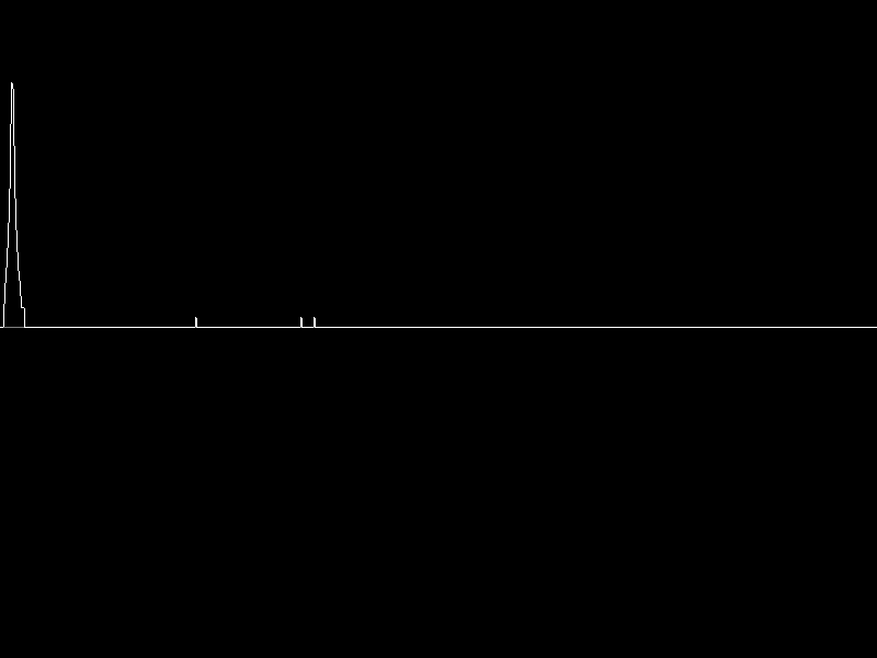 |
This figure shows what should be a split screen spectrogram and waterfall display. The spectrum on top appears about right, however the waterfall that’s supposed to exist in the bottom half of the display is completely absent.
Well, the good news is that I could at least capture a bug.
The next step was to walk this bug backwards through the design. In this case, we’re walking backwards through Fig. 2 above and the first component to look at is the overlay module. It is possible for the overlay module to lose synchronization. This typically means either the overlay isn’t ready when the primary display is ready for it, or that the overlay is still displaying some (other) portion of its video. Once out of sync, you can no longer merge the two displays. The two streams then need to be resynchronized. That is, the overlay module would need to wait for the end of the secondary image (the image to be overlaid on top of the primary), and then it would need to stall the secondary image until the primary display was ready for it again.
However, the overlay module wasn’t losing synchronization.
No?
This was a complete surprise to me. This was where I was expecting the bug, and where most of my debugging efforts had been (blindly) focused up until this point.
Okay, so … let’s move back one more step. (See Fig. 2)
It is possible for the video waterfall reader to get out of sync between its two clocks. Specifically, one portion of the reader reads data, one line at a time, from the bus and stuffs it into first a synchronous FIFO, and then an asynchronous one. This half operates at whatever speed the bus is at, and that’s defined by the memory’s speed. The second half of the reader takes this data from the asynchronous FIFO and attempts to create an AXI stream video output from it–this time at the pixel clock rate. Because we are not allowed to stall this video output to wait for memory, it is possible for the two to get out of sync. In this case, the reader (pixel clock domain) is supposed to wait for an end of frame indication from the memory reader (bus clock domain, via the asynchronous FIFO), and then it is to stall the memory reader (by not reading from the asynchronous FIFO) until it receives an end of video frame indication from its own video reconstruction logic.
A quick check revealed that yes, these two were getting out of sync.
Here’s how the “out-of-sync” detection was taking place:
	initial	px_lost_sync = 0;
	always @(posedge pix_clk)
	if (pix_reset)
		px_lost_sync <= 0;
	else if (M_VID_TVALID && M_VID_TREADY && M_VID_HLAST)
	begin
		// Check when sending the last pixel of a line.  On this last
		// pixel, the data read from memory (px_hlast) must also
		// indicate that it is the last pixel in a line.  Further,
		// if this is also the last line in a frame, then both the
		// memory indicator of the last line in a frame (px_vlast)
		// and the outgoing video indicator (M_VID_VLAST) must match.
		if (!px_hlast || (M_VID_VLAST && !px_vlast))
			px_lost_sync <= 1'b1;
		else if (px_lost_sync && M_VID_VLAST && px_vlast)
			// We can resynchronize once both memory and
			// outgoing video streams have both reached the end of
			// a frame.
			px_lost_sync <= 1'b0;
	end
Following any reset, the entire design should be synchronized. That’s the easy part.
Next, if the output of the overlay
module
(that’s the M_VID_* prefix values) is ready to produce the last pixel of a
line, then we check if the FIFO signals line up. In our example, we have two
sets of synchronization signals. First, there are the M_VID_HLAST and
M_VID_VLAST signals. These are generated blindly based upon the frame size.
These indicate the last pixel in a line (M_VID_HLAST) and the end of a frame
(M_VID_VLAST) respectively–from the perspective of the video stream. Two
other signals, px_hlast and px_vlast, come through the
asynchronous FIFO. These
are used to indicate the last bus word in a line and the end of a frame from
the perspective of the data found within the
asynchronous FIFO
containing the samples read from memory–one bus word (not one pixel) at a time.
If these two ever get out of sync, then perhaps memory hasn’t kept up with the
display or perhaps something else has gone wrong.
So, to determine if we’ve lost sync, we check for it on the last pixel of any
line. That is, when M_VID_HLAST is true to indicate the last pixel in a
line, then px_last should also be true–both should be synchronized.
Likewise, when M_VID_VLAST (last line of frame) is true, then px_vlast
should also be true–or the two have come out of sync.
Because I’m also doing 128b bus word to 8b pixel conversions here, the two
signals don’t directly correspond. That is, px_hlast might be true (last
bus word of a line), even though M_VID_HLAST isn’t true yet (last pixel of a
line). Hence, I only check these values if M_VID_HLAST is true–on the last
pixel of the line.
That’s how we know if we’re out of sync. But … how do we get synchronized again?
For this, the plan is to read from the memory reader as fast as possible until the end of the frame. Once we get to the end of the frame, we’ll stop reading from memory and wait for the video (pixel clock) to get to the end of the frame. Once both are synchronized at the end of a frame, the plan is to then release both together and we’ll be synchronized again.
At least, that’s how this is supposed to work.
The key (broken) signal was the signal to read from the asynchronous
FIFO.
This signal, called afifo_read, is shown below.
	always @(*)
	begin
		afifo_read = (px_count <= PW || !px_valid
			|| (M_VID_TVALID && M_VID_TREADY && M_VID_HLAST));
		if (M_VID_TVALID && !M_VID_TREADY)
			afifo_read = 1'b0;

		// Always read if we are out of sync
		if (px_lost_sync && (!px_hlast || !px_vlast))
			afifo_read = 1'b1;
	end
Basically, we want to read from the asynchronous FIFO any time we don’t have a full pixel’s width left in our bus width to pixel gearbox, any time we don’t have a valid buffer, or any time we reach the end of the line–where we would flush the gearbox’s buffer. The exception to this is if the outgoing AXI stream is stalled. This is how the FIFO read signal is supposed to work normally. There’s one exception here, and that is if the two are out of sync. In that case, we will always read from the FIFO until the last pixel in a line on the last line of the frame.
This all sounds good. It looked good on a desk check too. II passed over this many times, reading it, convincing myself that this was right.
The problem is this was the logic that was broken.
If you look closely, you might notice that this logic would never allow us to get back in sync. Once we lose synchronization, we’ll read until the end of the frame and then stop, only to read again when any of the original criteria are true–the ones assuming synhronization.
Yeah, that’s not right.
This also explains why all my hardware traces showed the waterfall never resynchronizing with the outgoing video stream.
One missing condition fixes this.
	always @(*)
	begin
		// ...
		if (px_lost_sync && px_hlast && px_vlast && (!M_VID_HLAST
				|| !M_VID_VLAST))
			afifo_read = 1'b0;
	end
This last condition states that, if we are out of sync and we’ve reached the last pixel in a frame, then we need to wait until the outgoing frame matches our sync. Only then can we read again.
Once I fixed this, things got better.
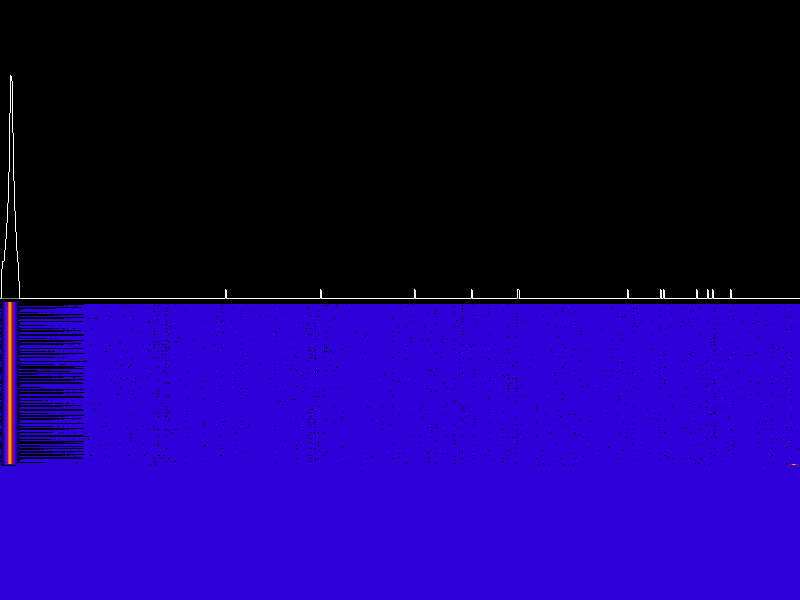 |
I could now get through a significant fraction of a frame before losing synchronization for the rest of it. In other words, I had found and fixed the cause of why the design wasn’t recovering, just not the cause of what caused it to get out of sync in the first place.
The waterfall background is also supposed to be black, not blue–so I needed to dig into that as well. (That turned out to be a bug in the QOI compression module. I could just about guess this bug, if I watched how the official decoder worked.)
So, back I went to the Wishbone scope, this time triggering the scope on a loss of sync event. I needed to find out why this design lost sync in the first place.
The Second Bug: How did we lose sync in the first place?
Years ago, I wrote an article that argued that good and correct video handling was all captured by a pair of counters. You needed one counter for the horizontal pixel, and another for the vertical pixel. Once these got to the raw width and height of the image, the counters would be reset and start over.
When dealing with memory, things are a touch different–at least for this design.
As hinted above, the bus portion of the waterfall
reader
works off of bus words, not pixels. It reads one line at a time from the
bus, reading as many bus words as are necessary to make up a line. In the case
of this system, a bus word on the Nexys Video
board
is 128-bits long–the natural width of the DDR3 SDRAM memory. (Our next
hardware
platform
will increase this to 512-bits.) Likewise, the waterfall pixel size is only
8-bits–since it has no color, and a false
color
will be provided later. Hence, to read an 800 pixel line, the bus master must
read 50 bus words (800*8/128). The last word will then be marked as the last
in the line, possibly also the last in the frame, and the result will be
stuffed into the asynchronous
FIFO.
Once the last word in a line is requested of the bus, the bus master
needs to increment his line pointer address to the next line
However, there’s a problem with bus mastering: the logic that makes requests of a bus has to take place many clocks before the logic that receives the bus responses. The difference is not really that important, but it typically ends up around 30 clock cycles or so. That means this design needs two sets of X and Y counters: one when making requests, to know when a full line (or frame) has been requested and that it is time to advance to the next line (or frame), and a second set to keep track of when the line (or frame) ends with respect to the values returned from the bus. This second set controls the end of line and frame markers that go into the synchronous and then asynchronous FIFO.
Let’s walk through this logic to see if I can clarify it at all.
-
First, there’s both an synchronous FIFO and an asynchronous one–since it can be a challenge to know the fill of the asynchronous FIFO.
-
Once the synchronous FIFO is at least half empty, the reader begins a bus transaction. For a Wishbone bus, this means both
CYCandSTBneed to be raised. -
For every
STB && !STALL, a request is made of the bus. At this time, we also subtract one from a counter keeping track of the number of available (i.e. uncommitted) entries in the synchronous FIFO. -
Likewise, for every
STB && !STALL, the IP increments the requested memory address.Once you get to the end of the line, set the next address to the last line start address minus one line of memory. Remember, we are creating a falling raster, where we go from most recent FFT data to oldest FFT data. Hence we read backwards through memory, one line at a time.
Once we get to the beginning of our assigned memory area, we wrap back to the end of our assigned memory area minus one line.
Once we get to the end of the frame, we need to reset the address to the last line the writer has just completed.
-
On evey
ACK, the returned by data gets stored into the synchronous FIFO. With each result stored in the FIFO, we also add an indication of whether this return was associated with the end of a line or the end of a frame. -
Once the reader gets to the end of the line, we restart the (horizontal)
pixelbus word counter and increment the line counter. When it gets to the end of the frame, we reset the line counter as well.Just to make sure that these two sets of counters (request and return) remain synchronized, the return counters to set to equal the request counters any time the bus is idle.
-
The IP then continues making requests until there would be no more room in the FIFO for the returned data. At this point,
STBgets dropped and we wait for the last request to be returned. -
Once all requests have been returned, drop
CYCand wait again.The rule of the bus is also the rule of the boarding house bathroom: do your business, and get out of there. Once you are done with any bus transactions, it’s therefore important to get off the bus. Even if we could (now) make more requests, we’ll get off the bus and wait for the FIFO to become less than half full again–that way other (potential) bus masters can have a chance to access memory.
And … right there is the foundation for this bug.
The actual bug was how I determined whether or not the last request was being
returned. Let’s look at that logic for a moment, shall we? Here’s what it
looked like (when broken): (Watch for what clears o_wb_cyc …)
	initial { o_wb_cyc, o_wb_stb } = 2'b00;
	always @(posedge i_clk)
	if (wb_reset)
		// Halt any requests on reset
		{ o_wb_cyc, o_wb_stb } <= 2'b00;
	else if (o_wb_cyc)
	begin
		if (!o_wb_stb || !i_wb_stall)
			// Drop the strobe signal on the last request.  Never
			// raise it again during this cycle.
			o_wb_stb <= !last_request;

		if (i_wb_ack && (!o_wb_stb || !i_wb_stall)
					&& last_request && last_ack)
			// Drop ACK once the last return has been received.
			o_wb_cyc <= 1'b0;
	end else if (fifo_fill[LGFIFO:LGBURST] == 0)
		// Start requests when the FIFO has less than a burst's size
		// within it.
		{ o_wb_cyc, o_wb_stb } <= 2'b11;

	always @(posedge i_clk)
	if (i_reset || !o_wb_cyc || i_wb_err)
		last_ack <= 0;
	else
		last_ack <= (wb_outstanding + (o_wb_stb ? 1:0)
				<= 2 +(i_wb_ack ? 1:0));
Look specifically at the last_ack signal.
Depending upon the pipeline, this signal can be off by one clock cycle.
This was the bug. Because the last_ack signal, indicating that there’s only
one more acknowledgement left, compared the number of outstanding requests
against 2 plus the current acknowledgment, and because the signal was
registered, last_ack might be set if there were two requests outstanding
and nothing was returned on the current cycle.
Since all requests would’ve been made by this time, the X and Y pixel
bus word counters for the request would reflect that we’d just requested a
line of data. The return counters, on the other hand, would be off by one
if CYC ever dropped a cycle early. These return counters would then get
reset to equal the request counters any time CYC was zero. Hence,
dropping the bus line one cycle early would result in a line
of pixels (well, bus words representing pixels …) going into the FIFO
that didn’t have enough pixels within it–or perhaps the LAST signal might
be missing entirely. Whatever the case, it didn’t line up.
This particular design was formally verified. Shouldn’t this bug have shown
up in a formal test? Sadly, no. It’s legal to drop CYC
early, so there’s
no protocol violation there. Further, my acknowledgment counter was off by
one in such that the formal properties allowed it. If I added an assertion
that CYC would never be dropped early (which I did once I discovered this
bug), the design would then immediately (and appropriately) fail.
There’s one more surprise to this story though. Why didn’t this bug show up in simulation?
Ahh, now there’s a very interesting lesson to be learned.
Reality: Why didn’t the bug(s) show up in simulation?
Why didn’t the bug show up earlier? Because of Xilinx’s DDR3 SDRAM controller, commonly known as “The MIG”.
I don’t normally simulate DDR3 memories. A DDR3 SDRAM memory controller requires a lot of hardware specific components, components that aren’t necessarily easy to simulate, and it also requires a DDR3 SDRAM simulation model. I tend to simplify all of this and just simulate my designs with an alternate SDRAM model–a model that looks and acts “about” right, but one that isn’t exact.
It was the difference between my simulation model, which wouldn’t trigger any of the bugs, and Xilinx’s MIG reality that ended up triggering the bug.
Fig. 11, for example, shows what the Wishbone scope returned when documenting the waterfall reader’s transactions with the MIG.
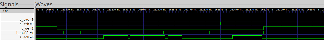 |
Focus your attention on first the stall (i_stall) and then the
acknowledgment (i_ack) lines.
First, stall is high immediately as part of the beginning of the transaction. This is to be expected. With the exception of filling a minimal buffer, any bus master requesting transactions of the bus is going to need to wait for arbitration. This only takes a clock or two. Once arbitration is received, the interconnect won’t stall the design again during this bus cycle.
Only the stall line gets raised again after that–several times even. These stalls are all due to the MIG.
Let’s back up a touch.
There are a lot of rules to SDRAM interaction. Most SDRAM’s are configured in memory banks. Banks are read and written in rows. The data in each row is stored in a set of capacitors. This allows for maximum data packing in minimal area (cost). However, you can’t read from a row of capacitors. To read from the memory, that row first needs to be copied to a row of fast memory. This is called “activating” the row. Once a row is activated, it can be read from or written to. Once you are done with one row, it must be “precharged” (i.e. put back), before a different row can be activated. All of this takes time. If the row you want isn’t activated, you’ll need to switch rows. That will cause a stall as the old row needs to be precharged and the new row activated. Hence, when making a long string of read or a long string of write requests, you’ll suffer from a stall every time you cross rows.
Xilinx’s MIG has another rule. Because of how their architecture uses an IO trained PLL (Xilinx calls this a “phasor”), the MIG needs to regularly read from memory to keep this PLL trained. During this time the memory must also stall. (Why the MIG can’t train on my memory reads, but needs its own–I don’t know.) These stalls are very periodic, and if you dig a bit you can find this taking place within their controller.
Then the part of the trace showing a long stalled section reflects the reality that, every now and again, the memory needs to be taken entirely off line for a period of time so that the capacitors can be recharged. This requires a longer time period, as highlighted in Fig. 12 below.
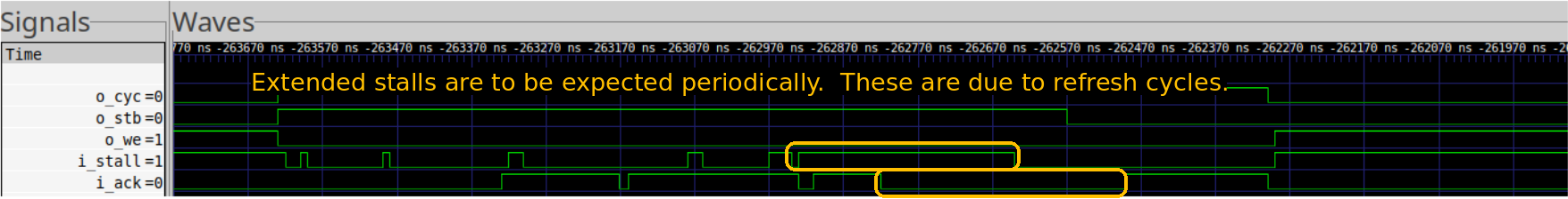 |
Once it’s time for a refresh cycle like this, several steps need to take place in the memory controller–in this case the MIG. First, any active rows need to be precharged. Then, the memory is refreshed. Finally, you’ll need to re-activate the row you need. This takes time as well–as shown in Fig. 12.
That’s part one–the stall signal. My over-simplified SDRAM memory model doesn’t simulate any of these practical memory realities.
Part two is the acknowledgments. From these traces, you can see that there’s about a 30 cycle latency (300ns) from the first request to the first acknowledgment. However, unlike my over-simplified memory model, the acknowledgments also come back broken due to the stalls. This makes sense. If every request takes 30 cycles, and some get stalled, then it only makes sense that the stalled requests would get acknowledged later the ones that didn’t get stalled.
Put together, this is why my waterfall display worked in simulation, but not in hardware.
Conclusion
Wow, that was a long story!
Yeah. It was long from my perspective too. Although the “bugs” amounted to only 2-5 lines of Verilog, it took a lot of work to find those bugs.
Here are some key takeaways to consider:
-
All of this was predicated on a simulation vs hardware mismatch.
Because the SDRAM simulation did not match the SDRAM reality, cycle for cycle, a key hardware reality was missed in testing.
-
This should’ve been caught via formal methods.
From now on, I’m going to have to make certain I check that
CYCis only ever dropped either following either a reset, an error, or the last acknowledgment. There should be zero requests outstanding whenCYCis dropped. -
Why wasn’t the pixel resynchronization bug caught via formal?
Because … FIFOs. It can be a challenge to formally verify a design containing a FIFO. Rather than deal with this properly, I allowed the two halves of the design to be somewhat independent–and so the formal tool never really examined whether or not the design could (or would) properly recover from a lost sync.
-
Did formally verifying the overlay module help?
Yes. When we went through it, we found bugs in it. Once the overlay module was formally verified, the result stopped jumping. Instead, the overlay might just note a problem and stop showing the overlaid image. Even better, unlike before the overlay module was properly verified, I haven’t had any more instances of the top and bottom pictures getting out of sync with each other.
-
What about that blue field?
Yes, the waterfall background should be black when no signal was present. The blue field turned out to be caused by a bug in the QOI compression module.
Once fixed, the captured image looked like Fig. 13 below.
 |
This was easily found and fixed. (It had to deal with a race condition on the pixel index when writing to the compression table, if I recall correctly …)
-
How about that QOI module?
The thing worked like a champ! I love the simplicity of the QOI encoding, enough so that I’m likely to use it again and again!
Okay, perhaps I’m overselling this. It wasn’t perfect at first. This is, in many ways to be expected–this was the first time it was ever used. However, it was small and cheap, and worked well enough to get the job done.
Some time later, I managed to formally verify the compression engine, and I found another bug or two that had been missed in my hardware testing.
That’s compression.
Decompression? That’s another story. I think I’ve convinced myself that I can do decompression in hardware, but the algorithm (while cheap) isn’t really straightforward any more. At issue is the reality that it will take several clock cycles (i.e. pipeline stages) to determine the table index for storing colors into, yet the very next pixel might be dependent upon the result of reading from the table. Scheduling the pipeline isn’t straightforward. (Worse, I have simulation test cases showing that the decompression logic I have doesn’t work yet.)
-
Are the displays ready for prime time?
I’d love to say so, but they don’t have labeled axes. They really need labeled axes to be proper professional displays. Perhaps a QOI decompression algorithm can take labeled image data from memory and overlay it onto the display as well. However, to do this I’m going to have to redesign how I handle scaling, otherwise the labels won’t match the image.
Worse, [DG3YEV Tobias] recently put my waterfall display to shame. My basic displays are much too simple. So, it looks like I might need to up my game.
I should point out, in passing, that the UberDDR3 SDRAM controller doesn’t nearly have as many stall cycles as Xilinx’s MIG. It doesn’t use the (undocumented) hardware phasors, so it doesn’t have to take the memory offline periodically. Further, it can schedule the row precharge and activation cycles so as to avoid bus stalls (when accessing memory sequentially). As such, it operates about 10% faster than the MIG. It even gets a lower latency. These details, however, really belong in an article to themselves.
I suppose the bottom line question is whether or not these displays are ready for our next testing session. The answer is a solid, No. Not yet. I still need to do some more testing with them. However, these displays are a lot closer now than they’ve been for the last two years.
Seest thou a man diligent in his business? he shall stand before kings; he shall not stand before mean men. (Prov 22:29)