
Bringing up Kimos
Ever had one of those problems where you were stuck for weeks?
It’s not supposed to happen, but … it does.
Let me tell you about the Kimos story so far.
What is Kimos?
Kimos is the name of one of the current open source projects I’m working on. The project is officially named the “Kintex-7 Memory controller, Open Source toolchain”, but the team shortened that to “KiMOS” and I’ve gotten to the point where I just call it “Kimos” (pronounced KEE-mos). The goals of the project are twofold.
-
Test an Open Source DDR3 SDRAM memory controller.
This includes both performance testing, and performance comparisons against Xilinx’s MIG controller.
Just as a note, Angelo’s controller has a couple of differences with Xilinx’s controller. One of them is a simpler “native” interface: Wishbone, with an option for one (or more) auxilliary wire(s). The auxilliary wire(s) are designed to simplify wrapping this controller with a full AXI interface. Another difference is the fact that Angelo’s controller is built using documented Xilinx IO capabilities only–rather than the
PHY_CONTROLandPHASER*constructs that Xilinx used and chose not to document.My hypothesis is that these differences, together with some internal structural differences that I encouraged Angelo to make, will make his a faster memory controller. This test will tell.
-
Once the memory controller works, our goal is to test Kimos using an entirely open source tool flow.
This open source tool flow would replace Vivado.
The project hardware itself is built by Enclustra. It consists of two boards: a Mercury+ ST1 baseboard, and an associated KX2 daughterboard. Together, these boards provide some nice hardware capability in one place:
-
There’s a large DDR3 SDRAM memory, with a 64b data width. Ultimately, this means we should be able to transfer 512b per FPGA clock. In the case of this project, that’ll be 512b for every 10ns (i.e. a 100MHz FPGA system clock)–even though the memory itself can be clocked faster.
-
The board also has two Gb Ethernet interfaces, although I only have plans for one of them.
Each interface (naturally) includes an MDIO management interface. Although I might be tempted to take this interface for granted, it shouldn’t be. It was via the MDIO interface that I was able to tell which of the two hardware interfaces corresponded to ETH0 on the schematic and which was ETH1.
-
There’s an SD card slot on the board, so I’ve already started using it to test my SDIO controller and it’s new DMA capability. Once tested, the dev branch (containing the DMA) will have been “tested” and “hardware proven”, and so I’ll be able to then merge it into the master branch.
-
I’m likely to use the FMC interface to test a new SATA controller I’m working on. A nice FPGA Drive daughter board from Ospero Electronic Design, Inc., will help to make this happen.
Do note, though, that this controller, although posted, is most certainly broken and broken badly at present–it’s just not that far along in its development to have any reliability to it. The plan is to first build a SATA Verilog model, get the controller running in simulation, and then to get it running on this Enclustra hardware. It’s just got a long way to go in its process at present. The good news is that the project is funded, so if you are interested in it, come back and check in on it later–after I’ve had the chance to prove (and therefore fix) it.
-
The device also has some I2C interfaces, which I might investigate for testing my ultimate I2C controller on. The main I2C bus has three chips connected to it: an Si5338 clock controller (which isn’t needed for any of my applications), an encrypted hash chip (with … poor documentation–not recommended), and a real time clock.
-
The design also has some of the more standard interfaces that everything relies on, to include Flash and UART–both of which I have controllers for already.
-
Although the baseboard has HDMI capabilities, Enclustra never connected the HDMI on the baseboard to the KX2 daughterboard. Hence, if I want video, I’ll need to use the DisplayPort hardware–something I haven’t done before, but … it does have potential (just not funding).
This is a shame, because I have a bunch of live HDMI displays that I’d love to port to this project that … just aren’t likely to happen.
Eventually, my plan is to port my SONAR work to this hardware–but that remains a far off vision at this point.
The project is currently a work in progress, so I have not gotten to the point of completing either of the open source objectives. (Since I initially drafted this, Angelo’s controller has now been ported, and appears to be working–it’s performance just hasn’t been measured yet.)
I have, however, completed a first milestone: getting the design working with Xilinx’s MIG controller. For a task that should’ve taken no longer than a couple of days, this portion of the task has taken a month and a half–leaving me stuck in FPGA Hell for most of this time.
Now that I have Xilinx’s MIG working, I’d like to share a brief description of what went wrong, and why this took so long. Perhaps others may learn from my failures as well.
The challenges with board bringup
The initial steps in board bringup went quickly: I could get the LEDs and serial port up and running with no problems. From there I could test the ZipCPU (running out of block RAM), and things looked good. At this point, a year or so ago, I put the board on the shelf to come back to it later when I had more time and motivation (i.e. funding).
I wasn’t worried about the next steps. I already had controllers for the main hardware components necessary to move forward. I had a controller that would work nicely with Xilinx’s MIG, another that would handle the Gb Ethernet, a flash controller, and so on. These were all proven controllers, so it was just a matter of integrating them and making sure things worked (again) as expected.
Once the Kimos project kicked off, with the goals listed above, I added these components to the project and immediately had problems.
The DONE LED
The first problem was that the “DONE” LED wouldn’t light. Or, rather, it would light just fine until I tried to include Xilinx’s MIG controller. Once I included Xilinx’s MIG controller into the design the LED would no longer light.
Now … how do you fix that one? I mean, where do you even start?
 |
I started by reducing the design as much as possible. I removed components from the design, and adjusted which components were in the design and which were not. With a bit of work, I was able to prove–as mentioned above–that the design would work as long as Xilinx’s MIG (DDR3 SDRAM) controller was not a part of the design. The moment I added Xilinx’s MIG, the design stopped working.
Ouch. What would cause that? Is there a short circuit on the board somewhere? Did I mess up the XDC file? The MIG configuration?
With some help from some other engineers, we traced the first problem to the open source FPGA loader I was using: openFPGALoader. As it turns out, this loader struggles to load large/complex designs at high JTAG frequencies. However, if you drop the frequency down from 4MHz to 3.75MHz, the loader will “just” work and the DONE LED will get lit.
The problem goes a bit deeper, and highlights a problem I’ve had personally as well: since the developer of the openFPGALoader component can’t replicate the problem with the hardware he has, he can’t really test fixes. Hence, although a valid fix has been proposed, the developer is uncertain of it. Still, without help, I wouldn’t have made it this far.
Sadly, now that the DONE LED lit up for my design, it still didn’t work. Worse, I no longer trusted the FPGA loader. This left me always looking over my shoulder for another loading option.
For example, I tried programming the design into flash and then using my internal configuration access port (ICAPE) controller to load the design from flash. This didn’t work, until I first took the flash out of eXecute in Place (XiP) mode. (Would I have known that, if I hadn’t been the one to build the flash controller and put it into XiP mode in the first place? I’m not sure.) However, if I first told the flash to leave XiP mode, I could then specify a warm-boot address to my ICAPE controller, followed by an IPROG command, which could then load any design that … didn’t include Xilinx’s MIG DDR3 SDRAM controller.
At this point, I had proved that my problem was no longer the openFPGALoader. That was the good news. The bad news was that the design still wasn’t working whenever I included the MIG.
JTAG/UART not working
If the design loads, the place I want to go next is to get an internal logic analyzer up and running. Here, I have two options:
-
Xilinx’s ILA requires a JTAG connection.
Without a Xilinx compatible JTAG connector, I can’t use Xilinx’s ILA.
At one point I purchased a USB based JTAG controller. I … just didn’t manage to purchase the right one, and so the pins never fit.
-
I typically do my debugging over UART, using a Wishbone scope–something we’ve already discussed on the blog. Using this method I can quickly find and debug problems.
However, with this particular design, any time I added the MIG SDRAM controller to the design my UART debugging port would stop working–together with the rest of the design. That left me with no UART, and no JTAG. Indeed, I could’ve ping’d the board via the Gb Ethernet unless and until I added the MIG.
Something was seriously wrong. This is definitely not “cooking with gas”.
So how then do you debug something this? LEDs!
LEDs not working
Debugging by LED is slow. It can take 10+ minutes to make a change to a design, and each LED will only (at best) give you one bit of output. So the feedback isn’t that great. Still, they are an important part of debugging early design configuration issues. In this case, the Enclustra KX2 daughterboard has four LEDs on it, and the Mercury+ ST1 baseboard has another 4 LEDs. Perhaps they could be used to debug the next steps?
 |
Normally, I build my designs with a “Knight Rider” themed LED display. This helps me know that my FPGA design has loaded properly. There are two parts to this display. First, there’s an “active” LED that moves from one end of the LED string to the other and then back again. This “active” LED is ON with full brightness–whatever that means for an individual design. Then, once the “active” LED moves on to the next LED in the string, a PWM (actually PDM) signal is used to “dim” the LED in a decaying fashion. Of course, the CPU can easily override this display as necessary.
My problem was that, even though the “DONE” LED would (now) light up when loading a design containing the MIG, these user LEDs were not doing anything.
Curiously, if I overrode the LEDs at the top level of the design, I could make them turn either on or off. I just couldn’t get my internal design to control these LEDs properly. (I call this an “override” method because the top level of my design is generated by AutoFPGA, and I wasn’t going so far as to adjust the original sources describing how these LEDs should ultimately operate.) Still, using this top-level override method, I was able to discover that I could see LEDs 4-7 from my desk chair, that these were how I had wired up the LEDs on the baseboard (a year earlier), and that LEDs 6 and 7 had an opposite polarity from all of the other LEDs on the board.
All useful, it just didn’t help.
At one point, I noticed that the LEDs were configured to use the IO standard
SSTL15 instead of the normal LVCMOS15 standard I normally use. Once I
switched from SSTL15 to LVCMOS15, my knight-rider
display worked.
Unfortunately, neither the serial port nor the Ethernet port worked. Both of these continued to work if the MIG controller wasn’t included in the design, just not if the MIG controller was included.
Voodoo Engineering
I like to define Voodoo engineering as “Changing what isn’t broken, in an attempt to fix what is.” Not knowing what else to try, I spent a lot of time doing Voodoo engineering just trying to get the design working.
-
With the help of a hardware friend and his lab, we examined all of the power rails. Could it be that the design was losing power during the startup sequence, and so not starting properly even though the “DONE” LED was lighting up?
No.
After a lot of work with various probes, all we discovered was that the design used about 50% more power when the MIG was included. Did this mean there was a short circuit somewhere?
Curiously, it was the FPGA that got warmer, not the DDR3 SDRAM.
I left this debug session convinced I needed to look for a bug in my XDC file somewhere.
-
I spent a lot of time comparing the schematic to the XDC file. I discovered some rather important things:
-
Some banks required internal voltage references. These were not declared in any of the reference designs.
-
Two banks needed DCI cascade support, but the reference design only had one bank using it.
-
The design required a voltage select pin that I wasn’t setting. This pin needed to be set to high impedance.
-
I had the DDR3 CKE IO mapped to the wrong pin.
-
-
The Enclustra ST1 baseboard can support multiple IO voltages. These need to be configured via a set of user jumpers, and the constraints regarding how these IO voltages are to be set are … complex. Eventually, I set banks A and B to 1.8V and bank C to 1.2V.
Sadly, nothing but the LEDs were using banks B and C, so … none of these changes helped.
I suppose I should be careful here: I was probably fixing actual bugs during these investigations. However, none of the bugs I fixed actually helped move me forward. Fixing these bugs didn’t get the UART+SDRAM working, nor did they get the network interface working whenever the SDRAM was included. Both of these interfaces worked without the SDRAM as part of the design, they just didn’t work when connecting the MIG SDRAM controller to the design.
Was there some short circuit connection between SDRAM pins and something on the UART or network IO banks? There shouldn’t be, I mean, both of these peripherals were on separate IO banks from the DDR3 SDRAM.
Reference design
At this point, I needed to use the reference design to make certain the hardware still worked. I’d had weeks of problems where the DONE pin wasn’t going high. Did this mean I’d short circuited or otherwise damaged the board? The design was using a lot more power when configured to use the SDRAM. Did this mean there was a short circuit damaging the board? Had my board been broken? Was there a manufacturing defect?
Normally, this is where you’d use a reference design. Indeed, this was Enclustra’s recommendation to me. Normally this would be a good recommendation. They recommended I use their reference design, prove that the hardware worked, and then slowly migrate that design to my needs. My problem with this approach was that their reference design wasn’t written in RTL. It was written in TCL with a Verilog wrapper. Worse, their TCL Ethernet implementation depended upon an Ethernet controller from Xilinx that … required a license. Not only that, Enclustra did not provide any master XDC file(s). (They did provide schematics and a .PRJ file with many of the IOs declared within it.) Still, how do you “slowly migrate” TCL to RTL? That left me with just their MIG PRJ file to reference and … I still had a bug.
There were a couple of differences between my MIG PRJ configuration file and their reference MIG configuration. My MIG PRJ configuration file used a 100MHz user clock, and hence a 400MHz DDR3 clock, whereas their reference file used an 800MHz DDR3 clock. (My design wouldn’t close timing at 200MHz, so I was backing away to 100MHz.) Could this be the difference?
Upon request, one of my teammates built a LiteX design for this board. (It took him less than 2hrs. I’d been stuck for weeks! How’d he get it going so fast? Dare I mention I was jealous?) This LiteX design had no problems with the DDR3 SDRAM–although it doesn’t use Xilinx’s MIG. I even had him configure this LiteX demo for the 400MHz DDR3 clock, and … there were no problems.
Given that the LiteX design “just worked”, I knew the hardware on my board still worked. I just didn’t know what I was doing wrong.
The final bug: the reset polarity
One difference between the MIG driven design and the non-MIG design (i.e. my design without a DDR3 SDRAM controller) is that the MIG controller wants to deliver both system clock and the system reset to the rest of the design. Any failure to get either a system clock or a system reset from the MIG controller could break the whole design.
So, I went back to the top level LEDs again. I re-examined the logic, and made sure LED[7] would blink if the MIG was held in reset, and LED[6] would blink if the clocks didn’t lock. This lead me to two problems. The first problem was based upon where I had my board set up: I couldn’t see LED[7] from my desk top with a casual glance. I had to make sure I leaned forward in my desk chair to see it. (Yes, this cost me a couple of debug cycles before I realized I couldn’t see all of the LEDs without leaning forward.) Once I could see it, however, I discovered the system reset wire was being held high.
Well, that would be a problem.
Normally, when I use the MIG controller, I use an active high reset. This time, in order weed out all of the possible bugs, I’d been trying to make my MIG configuration as close to the example/reference configuration I’d been given. That meant I set the design up to use an active-low reset–like the reference design. I had assumed that, if the MIG were given an active low reset it would produce an active low user reset for the design.
Apparently, I was wrong. Indeed, after searching out the Xilinx user guide, I can confirm I was definitely wrong. The synchronous user reset was active high.
Once I switched to an active high reset things started working. My serial port now worked. I could now read from memory over the UART interface, and “ping” the network interface of the device. Even better, my debugging interface now worked. That meant I could use my Wishbone scope again.
I was now “cooking with gas”.
Cleaning up
From here on out, things went quickly. Sure, there were more bugs, but these were easily found, identified, and thus fixed quickly.
-
While the design came up and I could (now) read from memory, I couldn’t write to memory without hanging up the design. After tracing it, this bug turned out to be a simple copy error. It was part of some logic I was getting ready to test which would’ve ran the MIG at 200MHz, and the design at 100MHz–just in case that was the issue.
This bug was found by adding a Wishbone scope to the design, and then seeing the MIG accept a request that never got acknowledged.
Yeah, that’d lock a bus up real quick.
I should point out that, because I use Wishbone and because Wishbone has the ability to abort an ongoing transaction, I was able to rescue my connection to the board, and therefore my connection to the bus, even after this fault. No, I couldn’t rescue my connection to the SDRAM without a full reset, but I could still talk to the board and hence I could still use my Wishbone scope to debug the problem. Had this been an AXI bus, I would not have had this capability without using some form of protocol firewall.
-
Other bugs were found in the network software. This was fairly new software, never used before, so finding bugs here were not really all that surprising.
At least with these bugs, I could use my network software together with my Verilator-based simulation environment. Indeed, my C++ network model allows me to send/receive UDP packets to the simulated design, and receive back what the design would return.
Like I said, by this point I was “cooking with gas”. It took about two days (out of 45) to get this portion up and running.
The one bug that was a bit surprising was due to a network access test that set the host software into an infinite loop. During this infinite loop, the software would keep writing to a debug dump, which I was hoping to later use to debug any issues. The surprise came from the fact that I wasn’t expecting this issue, so I had let the test run while I stepped away for some family time. (Supper and a movie with the kids may have been involved here …) When I discovered the bug, the debug dump file had grown to over 270GB! Still, fixing this bug was pretty routine, and there’s not a lot to share other than it was just another bug.
Lessons learned
There are a lot of lessons to be learned here, some of which I’ve done to myself.
-
All RTL
I like all RTL designs. I prefer all RTL designs. I can debug an all RTL design. I can adjust an all RTL design. I can version control an all RTL design.
I can’t do this with a TCL design that references opaque components that may get upgraded or updated any time I turn around. Worse, I can’t fix an opaque component–and Xilinx isn’t known for fixing the bugs in their designs. As an example, the following bug has been lived in Xilinx’s Ethernet-Lite controller for years:
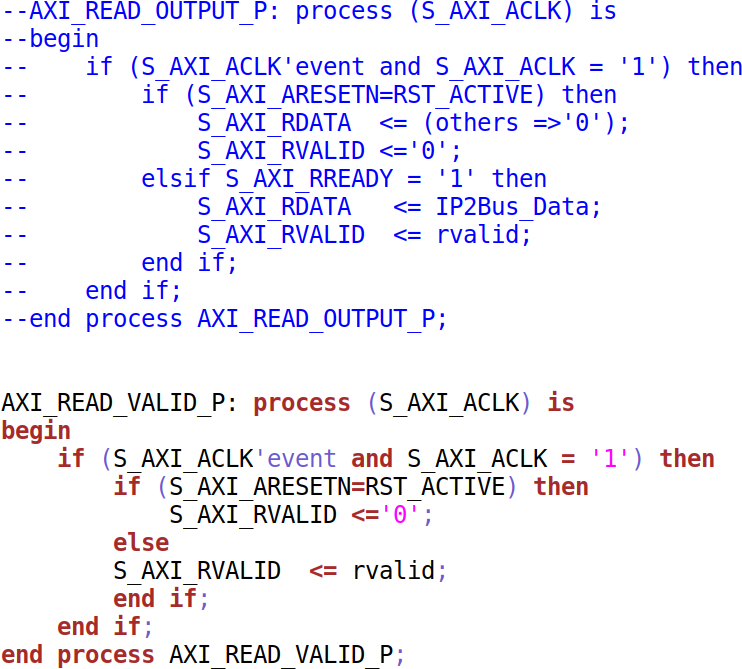 |
I reported this in 2019. This is only one of several bugs I found. The logic above is as of Vivado 2022.1. In this snapshot, you can see how they commented the originally broken code. As a result, the current design now looks like they tried to fix it and … it’s still broken on its face. (i.e. RVALID shouldn’t be adjusted or dropped unless RREADY is known to be true …)
Or what about RDATA?
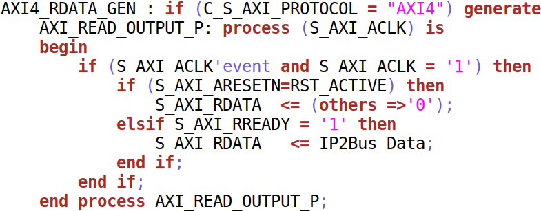 |
This also violates the first principles of AXI
handshaking. Notice that
RDATA might not get set if !RVALID && !RREADY–hence the first RDATA
value read from this device might be in error.
Yeah, … no. I’m not switching to Xilinx IP any time soon if I can avoid it. At least with my own IP I can fix any problems–once I find them.
For all of these reasons, I would want an all HDL reference design from any vendor I purchase hardware from. At least in this case, you can now find an all-Verilog reference design for the ST1+KX2 boards in my Kimos project–to include a working (and now open source) DDR3 SDRAM controller.
-
Simulation.
Perhaps my biggest problem was that I didn’t have an all-Verilog simulation environment set up for this design from the top level on down. Such an environment should’ve found this reset bug at the top level of the design immediately. Instead, what I have is a joint Verilog/C++ environment designed to debug the design from just below the top level using Verilator. This kept me from finding and identifying the reset bug–something that could have (and perhaps should have) been found in simulation.
In the end, after finding the reset bug, I did break down and I found a Micron model of a DDR3 memory. This was enough to debug some issues associated with getting the Wishbone scope working inside the memory controller, although it’s not really a permanent solution.
 |
Still, this is a big enough problem that I’ve been shopping around the idea of an open source all-Verilog simulation environment–something faster than Iverilog, with more capability. If you are interested in working on building such a capability–let me know.
-
Finger pointing
As is always the case, I tend to point the finger everywhere else when I can’t find a bug. This seems to be a common trait among engineers. For the longest time I was convinced that my design was creating a short circuit on the board. As is typically the case, I often have to come back to reality once I do find the bugs.
I guess the bottom line here is that I have more than enough humble pie to share. Feel free to join me.
Since writing this, the project has moved forward quite significantly. The design now appears to work with both the MIG and with the UberDDR3 controller–although I made some more beginner mistakes in the clock setup while getting that controller up and running. Still, it’s up and running now, so my next task will be running some performance metrics to see which controller runs faster/better/cheaper. (Hint: the UberDDR3 controller uses about 30% less logic, so there’s at least one difference right off the bat.)
Stay tuned, and I’ll keep you posted regarding how the two controllers compare against each other.
For I am not ashamed of the gospel of Christ: for it is the power of God unto salvation to every one that believeth; to the Jew first, and also to the Greek. (Romans 1:16)