
Why does blinky make a CPU appear to be so slow?
Imagine if you will that you’ve just built a brand new soft-core CPU. How fast do you think your brand-new soft-core CPU will be able to toggle a GPIO pin?
 |
The question is a fascinating one, and it applies to more than just home-brew soft cores. Several individuals for example have been surprised that the Xilinx MicroBlaze CPU can’t toggle a GPIO pin very fast. One individual measured his 82MHz MicroBlaze CPU toggling an IO pin at 37kHz. Another looked at his 80MHz MicroBlaze CPU, and measured his I/O toggle rate only at 2.5MHz. Still others measured a 100MHz MicroBlaze toggling an I/O at 1.7MHz or 2.3MHz. The problem isn’t unique to MicroBlaze either. Using a Zynq with a 250MHz bus clock, someone else measured the IO pins toggle frequency at no more than 3.8 MHz. Without insight into these architectures and their bus implementations, it’s hard to answer why these CPUs achieve the toggle rates they do.
This isn’t true of the ZipCPU. The ZipCPU’s implementation is entirely open and available for inspection. It’s not closed source. In other words, using an open source CPU like this one we should be able to answer the basic question, “Why do CPUs toggle I/O pins so slowly?” We might even get so far as to answer the question of, “How much I/O speed might I expect from a CPU?” But this latter question is really very CPU dependent, and we might be pushing our luck to answer it today.
So, let’s take a look at a basic GPIO controller. We can then run some tests on the ZipCPU, to see how fast the ZipCPU can toggle an LED from software.
A Basic GPIO controller
GPIO controllers are a dime a dozen. They are easy to build and easy to implement. If you are an FPGA developer and haven’t built your own GPIO controller before, then let me encourage you to do so as a good exercise.
For this article, I’ll just point out a couple features of the GPIO controller I use on many of my designs. If you are a regular reader of this blog, you’ll already know that I use the Wishbone Bus. You’ll also recognize the Wishbone I/O signals from our earlier article on the topic. So I’m not going to repeat those here.
My own GPIO controller, one I call WBGPIO, handles up to 16 inputs and 16 outputs as part of a single 32-bit register. The top 16-bits are input bits, whereas the bottom 16 are output bits. Not all of these bits need to be wired in any given design. Further, all of the input/output wires have fixed directions in this controller. I basically judged that, at least on an FPGA, by the time you’ve wired everything up to build your design you already know which direction the pins need to go.
The OpenRISC ecosystem offers a nice alternative if you want to examine a controller where the pins have a programmable direction, but I digress.
In the WBGPIO controller, adjusting an output bit requires writing to two bits in the control word at once. First, you want to set the new value of the bit, but second, in order to avoid the need to set all of the other output bits, you also need to set a second bit in the upper half of the register. The software supporting this controller, therefore includes the definitions:
#define GPIO_SET(WIRE)		(((WIRE)<<16)|(WIRE))
#define GPIO_CLEAR(WIRE)	((WIRE)<<16)
This means that we can set a bit,
*_gpio = GPIO_SET(LED0);or even clear the same bit,
*_gpio = GPIO_CLEAR(LED0);without needing to first read the register and adjust the one bit of interest, as in,
	// This is not the WBIO approach:
	//
	// Setting a bit without hardware support
	*_gpio = (*_gpio) | LED0;
	// Clearing a bit without hardware support
	*_gpio = (*_gpio) & ~LED0;
The Verilog logic necessary to handle this is trivially simple to write,
initial o_gpio = DEFAULT_OUTPUTS;
always @(posedge i_clk)
if ((i_wb_stb)&&(i_wb_we))
	o_gpio <= (o_gpio & ~i_wb_data[31:16])
		| (i_wb_data[15:0] & i_wb_data[31:16]);
The input logic is really irrelevant to our discussion today, but it’s not much more than a 2FF synchronizer.
reg	[31:0]	p_gpio;
reg	[15:0]	r_gpio;
always @(posedge i_clk)
	{ r_gpio, p_gpio } <= { p_gpio, i_gpio };
A quick check for anything changing can be used to create a GPIO interrupt,
always @(posedge i_clk)
	o_int <= (r_gpio != p_gpio[31:16]);
… or at least something like that. The actual implementation tries to
free up as much logic as
possible
by only adjusting a parameterizable NOUT output bits and only
reading and testing for changes from NIN input bits.
It really is just that basic.
The logic is also fast. As you can see, it only takes a single clock cycle to toggle any output pins. Surely this wouldn’t slow a CPU down, right?
Running a ZipCPU program
If you are interested in trying out the ZipCPU in simulation, the ZBasic repository is one of the better repositories for that purpose. Sure, I have other repositories tailored for specific boards, but this one is fairly generic.
To support this test, I recently added the WBGPIO module to the repository, as well as the WBGPIO AutoFPGA configuration file. One run of AutoFPGA, and this new module has been merged: new I/Os are created at the top level, the main.v file now connects it to my Wishbone bus, the GPIO control register has been added to the list of host accessible registers, and the CPU’s hardware definition header file now includes the defines necessary to access this peripheral.
Pretty neat, huh?
If you want to test it, you’ll need to build the
ZipCPU’s
tool chain.
You’ll find instructions for building the toolchain
here.
Once built, you should have zip-gcc in your path.
I placed a gpiotoggle.c program in the sw/board directory for you, and adjusted the makefile so it should build one of several tests for us. Feel free to examine that program, and adjust it as you see fit should you wish to repeat or modify this test.
Once you build gpiotoggle,
you’ll then want to start the simulation. The easiest way is to run
main_tb from from the
sim/verilated
directory, and to instruct it to load and run the
gpiotoggle
program.
% cd sim/verilated
% main_tb -d ../../sw/board/gpiotoggle
The -d flag above turns on the internal debugging options. In particular,
it tells the simulator to create a VCD
trace
file output that will be placed into trace.vcd.
Since the program will go on forever, you’ll need to press a control-C to kill it. On my ancient computer, about five seconds is all that is required to create 250MB file, which should be completely sufficient for our needs today.
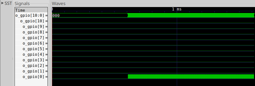
Once killed, you can pull the VCD trace file up in GTKWave to see how fast the LED toggled.
% gtkwave trace.vcdOnce you have the trace up, pull in the o_gpio trace at the top level
and expand it. You should get something like Fig. 2.
 |
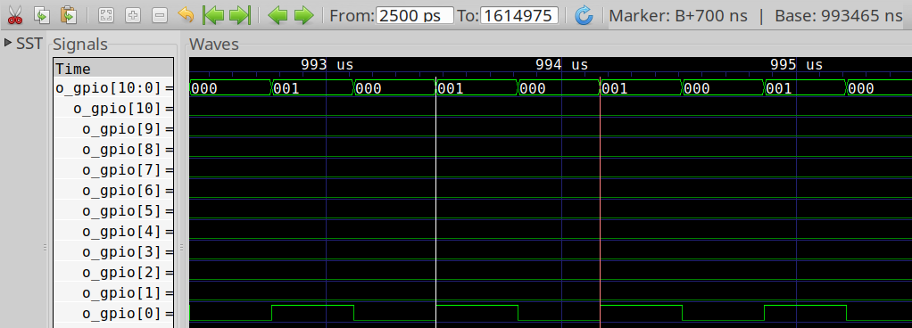
Don’t forget, you’ll have to scan past the program getting loaded by the
bootloader
to get to the point where the I/O is toggling. If you zoom into this
section where o_gpio[0] toggles, you should see something like Fig. 3 below.
 |
Shall we see how fast we can toggle this pin?
Running our Experiments
Let’s run some experiments. We’ll start slow, with the CPU’s pipeline disabled, and then slowly enable features along the way.
Before starting, though, let me ask you to do one thing: take out a piece of paper, and write onto it the fastest speed you expect the CPU to be able to toggle the I/O pin, assuming that the CPU is running at 100MHz.
Why 100MHz? Well, it’s sort of my baseline system clock speed, dating back to my work on the Basys3. Since the Basys3 offered a 100MHz clock input, I got used to using that speed for development. The reality is that some FPGAs will run slower, such as the Spartan 6 or the iCE40, and some will run faster. One individual even reported running the ZipCPU at 150MHz. 100MHz just happens to be a nice number in between that makes reading data from a trace file easier–since each clock tick is 10ns.
Now, fold that paper up with your prediction on it, and then let’s continue.
Starting out slow
Let’s start out as slow as we can, just to see how things improve by
adding more logic to our design. If you go into the file
rtl/cpu/cpudefs.v,
you can edit the
ZipCPU’s
default configuration. Let’s start by uncommenting the line defining
OPT_SINGLE_FETCH. We’ll also comment the OPT_EARLY_BRANCHING definition,
and so disable it. This is almost the lowest logic configuration of the
ZipCPU.
We’ve just turned off the
ZipCPU’s
pipeline logic,
we’ve
turned off all caches and the pipelined data access mode.
(More about pipelined data access in a moment.) If we wanted, we could also
disable the multiply and divide instructions, but those should be irrelevant
for the purposes of today’s test.
Go ahead and rebuild the design now, by typing make from the root directory.
% # cd to the root directory, then
% make
Now let’s look at our LED toggling program. The program contains many different approaches to toggling the LED. We’ll work through them one at a time. We’ll start by using the following loop to toggle the LED.
int main(argc, argv) {
	int	gpiocmd = 1<<16;
	while(1) {
		*_gpio = gpiocmd;
		gpiocmd ^= 1;
	}
}
Notice that, because of how we built our WBGPIO controller, we don’t need to read from the output port prior to writing the new value in order to ensure that we only toggle a single bit.
I shouldn’t have to mention that for any type of test of this type, you need
to turn compiler optimizations on with -O3. Without optimization, this
little snippet of code will turn into,
00e00000 <main>:
  ; Create a stack frame, and save some registers to it so they can be
  ; recovered later.
  e00000:	e8 14 85 0c 	SUB        $20,SP         | SW         R0,$12(SP)
  e00004:	64 c7 40 10 	SW         R12,$16(SP)
  ; Now create a stack frame where our local variables may be stored
  e00008:	63 43 40 0c 	MOV        $12+SP,R12
  ; Save a copy of argc and argv (we won't be using them anyway
  e0000c:	0c c7 3f f8 	SW         R1,$-8(R12)
  e00010:	14 c7 3f f4 	SW         R2,$-12(R12)
  ; gpiocmd = 0x10000, or 65536.  Load this into a register, then store it into
  ; the stack location for gpio
  e00014:	0e 01 00 00 	LDI        $65536,R1
  e00018:	0c c7 3f fc 	SW         R1,$-4(R12)
  ; Load the address of our GPIO register into R1
  ; This is also the first instruction within our our while(1) loop
  e0001c:	0a 00 03 00 	LDI        0x00c0000c,R1  // c0000c <_kram+0xc0000c>
  e00020:	0a 40 00 0c
  ; Load gpiocmd into R0, and write that to the GPIO register
  e00024:	84 e4 85 88 	LW         -4(R12),R0     | SW         R0,(R1)
  ; Load gpiocmd back into R0, and XOR it with one
  e00028:	04 87 3f fc 	LW         -4(R12),R0
  e0002c:	01 00 00 01 	XOR        $1,R0
  ; Write the result back into gpiocmd
  e00030:	04 c7 3f fc 	SW         R0,$-4(R12)
  ; and loop back to the top of our while loop
  e00034:	78 83 ff e4 	BRA        @0x00e0001c    // e0001c <main+0x1c>_
Each instruction takes, at a minimum, one cycle. You’ll see in a moment how difficult it can be to fetch each of these many instructions.
Part of the problem with this unoptimized implementation is that all of the
data values are kept in a local variable space in memory, never in any
registers. As you’ll also see below, each SW (store word) instruction
to write our gpiocmd variable to memory can take many clock cycles.
Loads are worse, since the
ZipCPU
needs to wait for a load to complete before continuing.
In other words, this is a very slow way to toggle an
I/O,
On the other hand, if you place variables into registers, such as placing
gpiocmd into R1, you’ll get much faster code. GCC’s -O3 applies
three levels of optimizations doing just this, so don’t forget to use it.
In this example, if you run a “make gpiotoggle.txt” from within the
sw/board directory,
you’ll get both an optimized executable as well as a
ZipCPU
disassembly file. If you look through that file, you can find
the main program generated from our C-code above. I added some comments to it
below, to help it make more sense to a reader.
00e00000 <main>:
  ; gpiocmd = (1<<16)
  e00000:       0e 01 00 00     LDI        $65536,R1
  ; R2 = _gpio, the address of the WBGPIO's one control register
  e00004:       12 00 03 00     LDI        0x00c0000c,R2  // c0000c <_kram+0xc0000c>
  e00008:       12 40 00 0c
  ; Here's the first instruction of our while loop: *_gpio = gpiocmd;
  e0000c:       0c c4 80 00     SW         R1,(R2)
  ; Now we toggle the bottom bit, gpiocmd ^= 1;
  e00010:       09 00 00 01     XOR        $1,R1A
  ; And repeat back to the beginning of our loop
  e00014:       78 83 ff f4     BRA        @0x00e0000c    // e0000c <main+0xc>
Within this main program are three instructions: one store instruction to
set the I/O, one XOR instruction to toggle the lower bit of the register R1
containing our gpiocmd, and then a
branch
always instruction to return to the top of the loop.
This looks much better than the unoptimized version!
So, let’s see … a quick back of the envelope estimate says that if we are
running at a 100MHz clock, these three instructions should take 10ns each,
so we should be able to toggle our LED every 30ns, right?
In this case, with OPT_SINGLE_FETCH defined, it takes 350ns to toggle
the LED once, or 700ns per cycle. The
I/O pin
therefore toggles at 1.4MHz.
Wow. What just happened?!
If you examine a VCD trace, you’ll see something like Fig. 4 below.
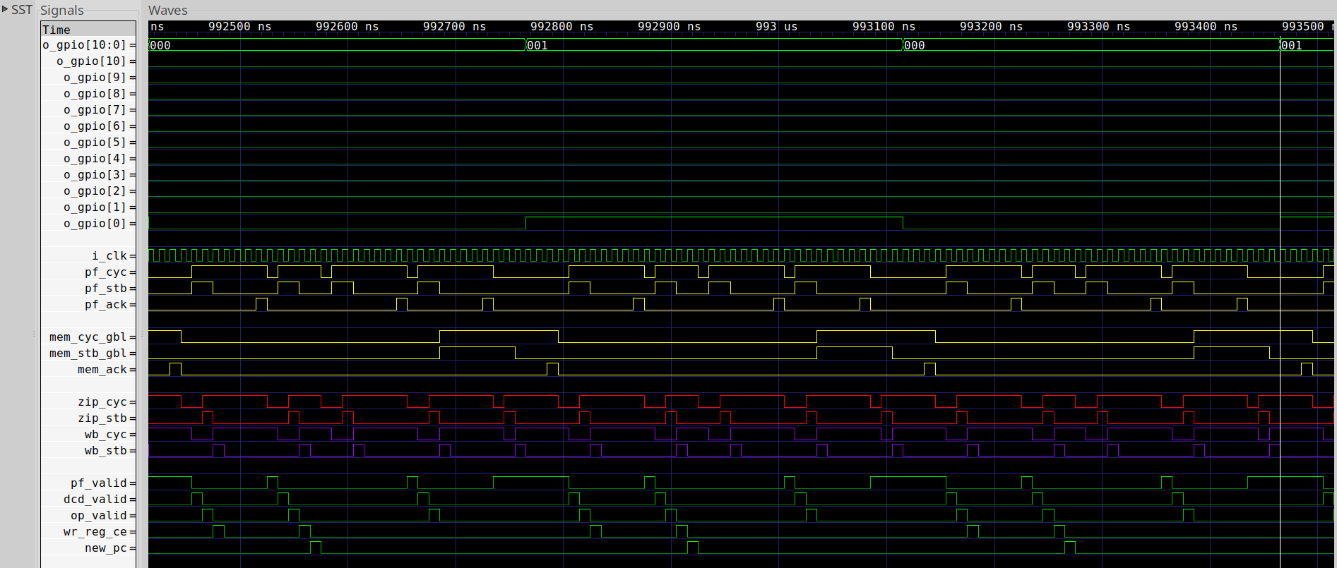 |
The trace can be rather confusing
to understand. First, you need to know the meanings of the various
bus signals,
the names of the four bus interfaces shown, mem_ (the CPU
memory controller),
pf_ (the CPU
prefetch),
zip_ (the combined memory/prefetch bus), and wb_ (the master
bus
within the system), as well as the
CPU pipeline signals
such
as pf_valid (there’s a valid instruction coming out of the prefetch stage),
dcd_valid (a valid instruction has come out of the instruction decoder),
op_valid (operands are ready to be used by the execution units) and
wr_reg_ce (a value may now be written to the register file). At the end of all
of that is the new_pc signal indicating that a
branch
has been detected at the end of the pipeline.
While I covered the basics of what these signals meant before, the overall trace can be difficult to follow. Therefore, I’ve summarized the signals from this trace in Fig. 5 below–to make for easy reading. You should also be able to click on the figure for an expanded version that might be easier to view.
 |
Basically, any time there’s an instruction at the output of a particular stage, instead of just listing the stage valid signal, I’ve also placed the instruction’s name into the figure as well–so you can see the instruction work its way through the pipeline.
So let’s spend some time examining Fig 5.
This trace basically shows just one cycle in this loop.
Within the trace, you can see the three instructions of our loop marked as
SW, XOR, and BRA respectively.
The timing within this trace is driven primarily by the
prefetch,
shown in the I-Bus line at the top. (This captures the pf_cyc and
pf_stb lines from Fig. 4 further up.)
We discussed this particular prefetch and how it
works
some time ago. In
that discussion,
I showed some clearer timing diagrams when illustrating how it would work.
In this chart, I’ve now collapsed the CYC & STB signal into the STB line,
the CYC & ACK signal into the ACK cycle and WAIT in between for those
times when CYC & !STB & !ACK.
But, why are their four wait cycles? To answer that question, let me direct your attention to Fig. 6 to the right.
 |
In this figure, you can see that the ZipCPU’s prefetch starts a memory cycle by setting its cycle and strobe lines. It then takes one clock cycle to arbitrate between the CPU and the debugging bus, creating a STB signal that actually gets broadcast across the bus. As currently configured, the block RAM memory takes two cycles to return. While we could drop this to one cycle, the memory was configured for two cycles in this test. One cycle would be just one clock faster on every memory operation. The next problem is in the interconnect where we have to select a result from among many items that might respond. Hence, an additional clock is taken to multiplex among these many possible answers. Finally, there’s an additional clock cycle to get our data back into the CPU.
Why are so many clocks involved? Are they required?
 |
To answer this question, let’s look at the bus structure for the ZBasic design, shown on the left.
The ZipCPU in this figure contains two Wishbone bus drivers. Because the ZipCPU is a Von Neumann architecture, there is only one bus interface leaving the CPU. (Not shown in the picture is a second arbiter dealing with the DMA in the ZipSystem.) Once the bus leaves the CPU, it is then merged with the debugging bus. An arbiter then selects between the two bus masters. However, by this point in time there’s now been too much combinatorial logic for the clock period. In order to maintain a high clock speed, a delay needs to be inserted on the path to the primary bus.
This gets us to the master bus strobe.
But what about the delay in the acknowledgement?
The purpose of the acknowledgment delay is basically the same thing: to reduce the necessary amount of logic within one clock period. In particular, our bus implementation contains a large case statement controlling the return data.
	always @(posedge i_clk)
	begin
		casez({		scope_sdcard_ack,
				flctl_ack,
				sdcard_ack,
				uart_ack,
				rtc_ack,
				wb_sio_ack,
				bkram_ack	})
			7'b1??????: wb_idata <= scope_sdcard_data;
			7'b01?????: wb_idata <= flctl_data;
			7'b001????: wb_idata <= sdcard_data;
			7'b0001???: wb_idata <= uart_data;
			7'b00001??: wb_idata <= rtc_data;
			7'b000001?: wb_idata <= wb_sio_data;
			7'b0000001: wb_idata <= bkram_data;
			default: wb_idata <= flash_data;
		endcase
	end
This takes time. To keep the CPU speed up, this case statement was given it’s own clock period. Indeed, there’s yet another clock taken to get back through the bus delay.
Hence, when you count it all out, fetching an instruction using this prefetch takes five cycles within this deslgn.
So, why were there six cycles shown in the trace in Fig. 5 above? Because an extra cycle was used within the priority prefetch/memory arbiter. That priority arbiter defaults to offering access to the memory unit over the prefetch. An extra clock is required to switch from data to prefetch access. This makes perfect sense when the ZipCPU’s prefetch uses an instruction cache, but the priority probably needs to switch when it isn’t.
 |
The timing associated with accessing the GPIO device to toggle the LED is similar. The big difference is that there’s only a single clock delay within the GPIO device.
Still, 1.4MHz is a good start. Let’s consider this the pretest: we can do better. The only problem is that doing better will cost us more logic. Therefore, we’ll need to adjust our configuration option(s) to control how much logic will be used.
Adding a better fetch routine
Some time ago, I discussed how to build a prefetch that would fetch two
instructions at once.
Let’s take a look at the difference we might expect by using this “better”
prefetch
unit.
To enable this second/alternate
prefetch,
we’ll comment the OPT_SINGLE_FETCH option and uncomment the
OPT_DOUBLE_FETCH option from within the CPU configuration
file.
An example trace from this updated configuration is shown above in Fig. 9 below.
 |
The big difference between this trace and the one in Fig. 5 above is that the prefetch strobe signals are now three cycles long, and there are two acknowledgement cycles. Given that the first strobe cycle deals with the priority arbiter focusing on data access instead of the instruction fetch, we’re still fetching two instructions in eight cycles now instead of one instruction in seven cycles. Clearly doubling the speed of the prefetch should speed up our algorithm, right?
Well, yes, just not much. We went from taking 700ns down to 580ns per cycle.
What happened? Why aren’t we going any faster?
In this case, the problem is the fact that the CPU isn’t fully pipelined,
Yes, the ZipCPU is a fully pipelined CPU. This requires multiple copies of the internal CPU data structures–one per pipeline stage. This also requires some rather elaborate stall calculation logic. To create a non-pipelined CPU, such as we have been testing so far, the pipeline stall logic has been simplified and many of the stages share data. In other words: the CPU’s instructions take several exclusive clock cycles to complete in this mode.
The next problem is that the XOR instruction has to wait at the output of the
prefetch
until it has been accepted into the
decode unit.
This will keep the
prefetch
from getting another instruction until the XOR has moved
into the decode operands stage.
As you might expect, the store word instruction takes five cycles on the data bus to finally complete. This means that we took a whole eight cycles to execute this one instruction before the next instruction could enter the instruction decode stage.
Sure, the XOR instruction executes faster, taking only four clocks,
but during this time the CPU
is waiting for the memory cycle to complete before starting this
instruction.
Worse, the BRA instruction cannot be fetched until the CPU accepts
the XOR instruction from the
prefetch.
When the next instruction is finally available, it’s a
branch always
instruction (BRA). When this instruction gets to the write-back stage, the
prefetch
has to reset itself and start fetching the next instruction from a new
address: the result of the branch. This also means we just aborted an ongoing
prefetch
memory operation for the instruction that would’ve followed the BRA
operation, had it not been a
branch.
In all, we are now taking 290ns for three instructions, or just under ten
clocks per instruction.
At this rate we can toggle our LED at 1.7MHz.
That doesn’t feel like much of an improvement over the last prefetch implementation.
What if we turned on the CPU’s pipelining logic? Would that help?
Going full pipeline
Pipelining allows the ZipCPU to execute multiple instructions at the same time. To do this, instruction processing is split into stages, with the effect that multiple instructions can be processed at once–with one instruction in each pipeline stage.
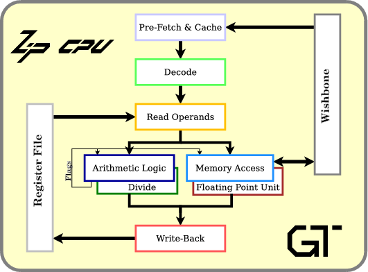 |
As you may recall, the
ZipCPU
has five basic pipeline
stages:
prefetch, decode,
read-operands,
execute ALU/mem/divide,
and write-back, as shown in Fig. 10 on the right. In general,
each instruction takes one clock cycle to work through each stage,
although most of my charts today just show when the outputs of all the given
stages are valid, with the exception that the WB (write-back) line shows when
the input of the write-back stage is valid.
All that said, if you execute multiple instructions at once, the result should be faster, right?
Let’s find out!
In order to enable the CPU
pipeline
in the configuration
file,
both the OPT_DOUBLE_FETCH
and the earlier OPT_SINGLE_FETCH options need to be commented out. This
also enables the instruction
cache,
in order to be able to feed the
CPU
enough instructions to keep it busy. Just to give us something to examine
later, let’s also turn off the
data cache,
early branching, and the
ZipCPU’s
pipelined bus
capability. (More on that later.) We can do this by commenting the
OPT_EARLY_BRANCHING and OPT_PIPELINED_BUS_ACCESS configuration options.
Turning off the
data cache
is a bit more difficult, since it requires setting LGDCACHE to zero in the
ZipCPU’s
AutoFPGA
configuration file
and then rerunning
AutoFPGA.
Once done, we can run our three instruction loop again.
You can see the basic results in the trace shown in Fig. 11 below.
 |
Wait, I thought CPU pipelines were supposed to be able to execute with one instruction in every stage? What’s with all the empty stages?
We’ll pick up the story after the branch instruction gets into the write-back stage. This forces the pipeline to be cleared, so all the work we’ve done on any subsequent instructions needs to be thrown away.
Ouch! That’ll slow us down.
Second, in addition to killing our
pipeline,
we also suffer a clock in the instruction
cache
due to switching between cache lines. This manifests itself in an extra clock
before SW shows on the PF line, as well as an extra clock between the
SW and XOR instructions on that same line. After the
branch,
our first instruction, SW is ready to move through our
pipeline
after two cycles. However, the cycle after SW is valid in the PF stage
is empty again. Why? Because we are again switching cache lines: SW is
the last instruction in a given cache line. Our
cache implementation
requires an extra instruction cycle when switching cache lines.
Why? Shouldn’t a cache be able to deliver one instruction per cycle?
Yes, perhaps it should. However, the cache tag is stored in block RAM. Therefore, it costs us one cycle to look up the cache tag, and a second cycle to compare if its the right tag. (I really need to blog about this.) With some optimization, we can skip this in the great majority of cases, but every now and then an access crosses cache lines and must suffer a stall.
Once we get to the XOR instruction, the instruction
cache
seems to be doing well.
A second optimization in the
ZipCPU’s
pipeline
implementation allows the XOR to complete before the SW instruction does.
This only works for store instructions, not data load instructions. Because
store instructions don’t modify any registers, the
ZipCPU
doesn’t need to hold the next instruction waiting for a result.
This optimization doesn’t apply to branch instructions however. Looking at this stall, I’m not sure I can explain it very well. I have a vague recollection of some complication forcing this, but I might need to go back and re-examine that stall logic. That’s the fun thing about examining traces in detail, though–you see all kinds of things you might not have been expecting.
Of course, since the early branching we’re going to discuss in the next section is such a cheap optimization, costing so few extra logic elements, that I hardly ever run the ZipCPU without it as we have just done here.
In the end, this took us 120ns to execute these three instructions
and toggle our LED, or 4 clock cycles per
instruction. This
leads to 240ns per LED cycle, or 4.2MHz. While this is better than
580ns per cycle, it’s still a far cry from the speed I’d expect from a
pipelined
CPU.
We can do better.
Early Branching
Perhaps you noticed in the last section all the instructions filling the pipeline that had to be thrown out when the branch instruction was encountered. This is unfortunate. Let’s do better in this section.
The ZipCPU has the capability of recognizing certain branch instructions from within the decode stage This allows the decode stage to send any branch always instructions directly to the prefetch. This also allows the pipeline to fill back up while the branch instruction bubble works its way through the pipeline.
In order to enable this early branching capability, we’ll uncomment and set
the OPT_EARLY_BRANCHING flag within the configuration file.
With this new configuration, we’re now down to 60ns per three
instructions
to toggle the I/O, or 120ns per cycle, for a cycle rate now of 8.3MHz.
You can see the resulting trace shown in Fig. 12 below.
 |
Unlike our previous figures, I’m now showing multiple toggles in this trace. Why? Because I can! The trace is now that short that I can fit multiple toggles in a single image.
The
trace
starts out much as before, with the SW, the stall, and then the
XOR and BRA instructions coming from the instruction
prefetch
unit.
This time, however, while the BRA instruction is in the decode stage, the
prefetch
stage is invalidated and the
cache
gets sent to get the next instruction in the loop.
While there appear to be some further room for optimization here, the data bus is now completely loaded. As a result, the only way we might go faster would be to speed up the data bus by, for example, simplifying the bus structure or removing some of the peripherals.
While 8.3MHz is much faster than we started, it’s still much slower than
the CPU’s
clock speed. Indeed, looking over our program, if our
CPU
had no stalls at all, we would only ever be able to do 60ns per cycle, or
16.6MHz.
Pipelined Multiple Bus Accesses
What if we wanted our CPU to toggle this LED faster? Speeding up the I-cache won’t help, nor would better branching logic. Right now, our bus is the bottleneck. It’s at its highest speed. Hence, we can’t push any more instructions into our CPU if we are stuck waiting four cycles for the bus cycle to complete. While we might be able to shave a clock cycle off in our bus implementation latency, doing that would essentially strip the ZBasic SoC down so bare that it could no longer be used for general purpose processing.
That leaves only one way to go faster: to stuff more than one store in each bus transaction.
The first step towards making this happen is to uncomment the
OPT_PIPELINED_BUS_ACCESS parameter in the
CPU configuration file,
and then to rebuild the
ZBasic
simulator.
This time, let’s update our
GPIO toggling
software
as well. Instead of using the XOR instruction, let’s instead issue
back-to-back set and clear instructions.
	while(1) {
		*_gpio = GPIO_SET(1);
		*_gpio = GPIO_CLEAR(1);
	}
This also compiles into a three instruction loop, like before, but this time it’s slightly different.
00e00000 <main>:
  e00000:       0a 00 03 00     LDI        0x00c0000c,R1  // c0000c <_kram+0xc0000c>
  e00004:       0a 40 00 0c
  e00008:       1e 01 00 01     LDI        $65537,R3
  e0000c:       13 40 df ff     MOV        $-1+R3,R2
  e00010:       9d 88 95 88     SW         R3,(R1)        | SW         R2,(R1)
  e00014:       78 83 ff f8     BRA        @0x00e00010    // e00010 <main+0x10>
In this case, we have two store instructions in a row followed by our branch always instruction. Further, the two store word instructions use the ZipCPU’s compressed instruction set encoding, so both are shown as part of the same instruction word.
The ZipCPU has a memory
controller
that has the ability to issue multiple subsequent memory
requests. This is the controller we just selected by enabling
OPT_PIPELINED_BUS_ACCESS. Issuing multiple
bus requests,
however, has some requirements in order to avoid crossing devices
and thus losing acknowledgments or getting any results out of order.
Specifically, multiple requests must be to the same identical, or to
subsequent, addresses. Hence these two store word instructions
will be placed into the same memory transfer.
To understand what that might look like, let’s take a look at Fig. 13 below.
 |
The first thing to notice is that we are now issuing two back to back store word requests of the bus. (The WB STB lines are high for two consecutive cycles, while the stall lines are low.) These two instructions fly through the bus logic in adjacent clock periods. Hence, when the acknowledgments come back, they are still together.
If you look down at the LED line, you’ll also notice the two changes are made
back to back. First the LED is set, then it is cleared. Then nothing happens
until the next
bus cycle.
This means we now have a duty cycle of only 14%. Sure, we’re
toggling faster, now at a rate of 70ns per cycle or equivalently at
a rate of 14MHz, but we now lost the 50% duty cycle we once had in our
original square wave.
Next, did you notice that the
prefetch
now issues a valid instruction immediately following the BRA instruction
from the decode
stage?
This is because we aren’t crossing cache lines anymore.
Further, did you notice the instructions highlighted in blue? These represent
the first half of the decompressed compressed instructions. Since the
prefetch
knows nothing about the compressed instruction encoding, all of the
prefetches control
state
is captured by the stall signal–independent of the blue marking. The
decoder
is the first to recognize the compressed instruction, and so I’ve then split
the store word instruction word into SW1 and SW2 representing the first
and second store word instruction respectively.
Finally, notice how the first SW instruction gets stuck in the read-operands
stage for an extra three cycles. This is due to the fact that the
memory unit
is busy, and so these commands cannot (yet) issue until the two memory
acknowledgements come back. Just to help illustrate this, I added the
data bus CYC signal back into my trace summary, outlining the time when the
bus
is busy. The first store instruction, SW1, cannot issue until this
memory cycle
finishes. Hence we are still limited by the
bus
speed.
Can we do better than 14MHz? What if we unrolled our loop a bit and so
packed eight store instructions per loop? Our C code would now look like,
	while(1) {
		*_gpio = GPIO_SET(1);
		*_gpio = GPIO_CLEAR(1);
		*_gpio = GPIO_SET(1);
		*_gpio = GPIO_CLEAR(1);
		*_gpio = GPIO_SET(1);
		*_gpio = GPIO_CLEAR(1);
		*_gpio = GPIO_SET(1);
		*_gpio = GPIO_CLEAR(1);
	}
with the associated assembly code,
00e00000 <main>:
  e00000:	0a 00 03 00 	LDI        0x00c0000c,R1  // c0000c <_kram+0xc0000c>
  e00004:	0a 40 00 0c
  e00008:	1e 01 00 01 	LDI        $65537,R3
  e0000c:	13 40 df ff 	MOV        $-1+R3,R2
  e00010:	9d 88 95 88 	SW         R3,(R1)        | SW         R2,(R1)
  e00014:	9d 88 95 88 	SW         R3,(R1)        | SW         R2,(R1)
  e00018:	9d 88 95 88 	SW         R3,(R1)        | SW         R2,(R1)
  e0001c:	9d 88 95 88 	SW         R3,(R1)        | SW         R2,(R1)
  e00020:	78 83 ff ec 	BRA        @0x00e00010    // e00010 <main+0x10>
How fast would you expect this loop to toggle our LED?
 |
As you can see from Fig. 14 above, we are now toggling our LED four times in
130ns, for a rough rate of 30MHz.
This is finally starting to look like we might expect from a CPU. We’re still taking a pretty big hit from the branch, which is also forcing the ongoing memory operation to be flushed.
Might we go further? Certainly! If you check the GPIO toggling
program,
there’s an example within it that now toggles our LED 72 times in 770ns.
At first I didn’t believe this would be possible, since the instruction
stream would now cross multiple cache lines. If the
pipeline
isn’t kept filled, the memory
controller
will break the extended memory cycle. However, in this case, because
there are so many compressed instructions, the extra cache cycles associated
with crossing cache lines aren’t noticed.
This gives us our ultimate LED toggling rate of 47MHz.
It’s also the time to check your notes. Remember how I asked you to scribble down the speed you expected at first, indicating how fast you felt a CPU could toggle a GPIO pin? Go ahead, take a peek at your scribbled note. How close did you come to the results we just presented?
Other Bus Implementations
I would be remiss if I didn’t point out two things regarding other implementations.
First, the Wishbone Classic implementation found in the Wishbone B3
specification
requires a minimum of three cycles per
bus
access, and doesn’t allow multiple transactions to be in flight at once.
At best, this would have limited us to 120ns per cycle and our 8.3MHz
number above. At worst, this will slow down the entire
SoC
operation from
100MHz down to 50MHz. However, this is the
bus
structure used by the OpenRISC
soft-core
CPU.
Second, while the AXI bus
is more universally accepted than the Wishbone
Bus,
Xilinx’s default AXI-lite
implementation
can’t handle once access per clock. At best, it can only do one access
every other clock. At that rate, your best speed would only ever be 90ns
per loop (assuming only two toggles, or one LED cycle per loop), not 70ns per
loop. Likewise, if you tried to do the 72 toggles per loop using
that demo AXI-lite
peripheral, you’d be stuck at 24MHz instead of the 47MHz mentioned above.
My whole point here is that if speed is important to you, then your choice of bus matters.
These same observations apply to your choice of interconnect implementation as well. However, without any insight into how the various SoC projects have implemented their interconnects, it’s a bit difficult to compare them.
Conclusions
We’ve now examined several implementations of blinky from the standpoint of the CPU. What sorts of conclusions can we draw? Perhaps the first and most obvious conclusion is that the speed of blinky depends. Just because your processor runs at 100MHz doesn’t mean you’ll be able to blink an LED at anywhere near that rate. The closest we managed to get was 47MHz.
-
Our first two examples showed how critical the prefetch’s performance is to overall CPU speed. Indeed, reality is usually worse than these examples. Our code above ran from an on-chip block RAM component. Had we been trying to read instructions from an external SRAM or even SDRAM, our performance would’ve likely been an order of magnitude worse.
-
We saw several examples of how an ongoing memory operation would bring the CPU to a halt. A really fast CPU, therefore, can only go as fast as its memory unit and bus will let it.
-
Pipelined CPU’s are commonly known for being able to retire one instruction per clock. Here we saw several examples where a pipelined CPU wasn’t able to retire one instruction per clock. . We saw examples where the prefetch couldn’t keep the pipeline filled with instructions, where an ongoing memory operation forced the pipeline to stall, and where a branch instruction forced the CPU to clear the pipeline.
All of these realities are known for keeping a CPU’s number of instructions per clock cycle lower than the ideal.
-
We saw the importance of a good early branching scheme. While the ZipCPU doesn’t really implement a traditional branch prediction scheme, it’s early branching mechanism can often compensate. Just adding this capability to our CPU under test nearly doubled its performance from 4.7MHZ to 8.3 MHz.
-
At one point, we got to the point where our performance was entirely dominated by the speed of a bus interaction. The CPU could run faster, but the bus could not. In many ways, I might argue that this test does more to measure a CPU’s bus speed than it measures the speed of the CPU. The only problem with that argument is that you can still mess up the speed of CPU implementation. Hence the I/O speed really depends upon both the speed of the CPU. as well as the speed of the bus.
-
We also learned that we could cheat the whole system if we could stuff multiple store requests into the same memory transaction, yielding our highest total toggle rate but yet distorting the square wave produced.
Finally, I should point out that computers aren’t optimized for toggling LEDs, so in many ways this is a very poor measure of how fast a CPU can perform. CPUs are optimized for executing instructions and for … interrupts! Multi-tasking! By the time you limit your CPU down to three instructions only, you’ve really destroyed the power your CPU had initially to execute arbitrary instructions, to execute diverse functions, to handle interrupts and more.
You might argue that this is like taking a semi-tractor, filling the trailer with a single loaf of bread, and taking it out onto the race track. That’s not what it was designed for!
On the other hand, if you really wanted to toggle an LED quickly, why not just do it from Verilog?
	initiali o_led = 1'b0;
	always @(posedge i_clk)
		o_led <= !o_led;
That design is a whole lot simpler than all the work we just spent to get our ZipCPU to toggle an LED at high speed, and it uses far fewer FPGA resources, while toggling our LED at a whole 50MHz!
And he gave some, apostles; and some, prophets; and some, evangelists; and some, pastors and teachers (Eph 4:11)