
Comparing the Xilinx MIG with an open source DDR3 controller
Last year, I had the wonderful opportunity of mentoring Angelo as he built an open source DDR3 SDRAM controller.
Today, I have the opportunity to compare this controller with AMD (Xilinx)’s Memory Interface Generator (MIG) solution to the same problem. Let’s take a look to see which one is faster, better, and/or cheaper.
Design differences
Before diving into the comparison, it’s worth understanding a bit about DDR3–both how it works, and how that impacts its performance. From there, I’d like to briefly discuss some of the major design differences between Xilinx’s MIG and the UberDDR3 controller.
We’ll start with the requirements of an SDRAM controller in general.
SDRAM in general
SDRAM stands for Synchronous Dynamic Random Access Memory. “Synchronous” in this context simply means the interface requires a clock, and that all interactions are synchronized to that clock. “Random Access” means that you should be able to access the memory in any order you wish. The key word in this acronymn, though, is the “D” for Dynamic.
“Dynamic” RAM is made from capacitors, rather than flip flops. Why? Capacitors can be made much smaller than flip flops. They also use much less energy than flip flops. When the capacitor is charged, the “bit” of memory it represents contains a “1”. When it isn’t, the bit is a zero. There’s just one critical problem: Capacitors lose their charge over time. This means that every capacitor in memory must be read and recharged periodically or it will lose its contents. The memory controller is responsible for making sure this happens by issuing “refresh” commands to the memory.
That’s only the first challenge. Let’s now go back to that “synchronous” part.
The original (non-DDR) SDRAM standard had a single clock to it. The controller would generate that clock and send it to the memory to control all interactions.
This was soon not fast enough. Why not send memory values on both edges of the clock, instead of just one? You might then push twice as much data across the interface for the same I/O bandwidth. Sadly, as you increase the speed, pretty soon the data from the memory doesn’t come back synchronous to the clock you send. Both the traces on your circuit board, as well as the time to complete the operation within the memory chip will delay the return signals so much that the returned data no longer arrives in time to be sampled at the source by the source’s clock before the next clock edge. Worse, these variabilities are somewhat unpredictable. Therefore, memories were modified so that they return a clock together with the data–keeping the data synchronous with the clock it is traveling with.
Sampling data on a returned clock can be a challenge for an FPGA. Worse, the returned clock is discontinuous: it is only active when the memory has data to return. This will haunt us later, so we’ll come back to it in a moment.
For now, let’s go back to the “dynamic” part of an SDRAM.
SDRAMs are organized into banks, with each bank of memory being organized into rows of capacitors. To read from an SDRAM, a “row” of data from a particular memory bank must first be “activated.” That is, it needs to be copied from its row of capacitors into a row of flip flops. From here, “columns” within this row can be read or written as desired. However, only one row of memory per bank can be active at any given time. Therefore, in order to access a second row of memory, the row in use must first be copied back to its capacitors. This is called “precharging” the row. Only then can the desired row or memory be copied to the active row of flip-flops for access.
I mentioned SDRAM’s are organized in “banks”. Each of these “bank”s can controlled independently. They each have their own row of active flip-flops. With few exceptions, such as the “precharge all rows” command, or the “refresh” cycle command, most of the commands given to the memory will be bank specific.
Hence, to read a byte of memory, the controller must first identify which bank the byte of memory belongs to, and from there it must identify which row is to be read. The controller must then check which row is currently in the flip-flop buffer for that bank (i.e. which row is active). If a different row is active, that row must first be precharged. If no row is active, or alternatively once a formerly active row is precharged, the controller may then activate the desired row. Only once the desired row is active can the controller issue a command to actually read the desired byte from the row. Oh, and … all of this is contingent on not needing to refresh the memory. If a refresh interrupt takes place, you have to precharge all banks, refresh the memory, and then start over.
Well, almost. There’s another important detail: Because of the high speeds we are talking about, the memory will return data in bursts of eight bytes. Hence, you can’t read just a single byte. The minimum read quantity is eight bytes in a single “byte lane”.
What if eight bytes at a time isn’t enough throughput for you? Well, you could strap multiple memory chips together in parallel. In this case, every command issued by the controller would be sent to all of the memory chips. All of them would activate rows together, all of them would refresh their memory together, and all of them could read eight bytes at a time. Each of these chips, then, would control a single “byte lane”. In our case today, we’ll be using a memory having eight “byte lanes”.
So, when it comes to the performance of a memory controller, what do we want to know? We want to know how long it will take us from when the controller receives a read (or write) request until the data can be returned from the memory chip. This includes waiting for any (potential) refresh cycles, waiting for prior active rows to be recharged, new rows to be activated, and the data to finally be returned. The data path is complex enough that we’ll need to be looking at these times statistically.
Specifically, we’re going to model transaction time as some amount of per-transaction latency, followed by a per-amount throughput.
Our goal will be to determine these two unknown quantities: latency and throughput. If we do our job well, these two numbers will then help us predict answers to such questions as: how long will a particular algorithm take, and how much memory bandwidth is available to an application.
MIG
Let’s now discuss some of AMD (Xilinx)’s DDR3 memory controller This is the controller generated by their “Memory Interface Generator” and affectionately known simply as the “MIG” or “MIG controller”.
AMD (Xilinx)’s MIG controller is now many years old. Judging by their change log, it was first released in 2013. Other than configuration adjustments, it has not been significantly modified since 2016. This is considered one of their more “stable” IPs. It gets a lot of use by a wide variety of users, and I’ve certainly used it on a large number of projects.
Examining the source code of the MIG reveals that it is built in two parts. This can be seen from Fig. 1 below, which shows how the MIG fits in the context of the entire test stack we’ll be using today.
 |
The first part of the MIG processes AXI transaction requests into its internal “native” interface. AXI, however, is a complex protocol. This translation is not instantaneous, and therefore takes a clock (or two) to accomplish. Many FPGA designers have discovered they can often improve upon the performance of the MIG by skipping this AXI translation layer and using the “native” interface instead. I have not done so personally, since I haven’t found sufficient documentation of this “native” interface to satisfy my needs–but perhaps I just need to look harder at what’s there.
One key feature of an AXI interface is that it permits a certain amount of transaction reordering. For example, a memory controller might prioritize two interactions to the same bank of memory, such that the interaction using the currently active row might go first. Whether or not Xilinx’s MIG does this I cannot say. For today’s test measurements, we’ll only be using one channel–whether read or write, and we’ll only be using a single AXI ID. As a result, all requests must complete in order, and there will be no opportunity for the MIG to reorder any requests.
DDR3 speeds also tend to be much faster than the FPGA logic the controller must support. For this reason, Xilinx’s DDR3 controller runs at either 1/2 or 1/4 the speed of the interface. This means that, on any given FPGA clock cycle, either two or four commands may be issued of the DDR3 device. For this test, we’ll be running at 1/4 speed, so four commands may be issued per system clock cycle.
The biggest problem Xilinx needed to solve with their controller was how to sample return data. Remember, the data returned by the memory contains a discontinuous clock. Worse, the discontinuous clock transitions when the data transitions. This means that the controller must (typically) delay the return clock by a quarter cycle, and only then clock the data on the edge. But … how do you know how far a quarter cycle delay is in order to generate the correct sample time for each byte lane?
Xilinx solved this problem by using a set of IO primitives that they’ve never fully documented. These include PHASORs and IO FIFOs. Using these IO primitives, they can lock a PLL to the returned data clock, and then use that PLL to control the sample time of the return data. This clock is then used to control a special purpose asynchronous FIFO. From here, the data is returned to its environment.
One unusual detail I’ve seen from the MIG is that it will often stall my read requests for a single cycle at a time in a periodic fashion. Such stalls are much too short for any refresh cycles. They are also more frequent than the (more extended) refresh cycles. This leads me to believe that Xilinx’s IO PLL primitive has an additional requirement, which is that in order to maintain lock, the MIG must periodically read from the DDR3 SDRAM. Hence, the MIG must not only take the memory offline periodically to keep the capacitors refreshed, it must also read from the memory to keep this IO PLL locked. Worse, it cannot read from the device at the same time it does this station keeping. As with the AXI to native conversion, this PLL station keeping requirement negatively impacts the MIG’s performance.
Before leaving this point, let me underscore that these “special purpose” IO elements were never fully documented. This adds to the challenge of building an open source controller, since the open source engineer must either reverse engineer these undocumented hardware components or build their data sampler in some other fashion.
Some time ago, I tried building a block-RAM based memory peripheral capable of handling AXI exclusive access requests. While trying to verify that the ZipCPU could generate exclusive access requests and that it would do so properly, I looked into whether or not the MIG would support them. Much to my surprise, the MIG has no exclusive access capability. I’ve since been told that this isn’t a big deal, since you only need exclusive access when more than one CPU is running on the same bus and the MicroBlaze CPU was never certified for multi–core operation, but I do still find this significant.
Finally, the MIG controller tries to maximize parallelism with various “bank machines”. These “bank machines” appear to be complex structures, allocated dynamically upon request. Each bank machine is responsible for handling when and if a row for a given memory bank must be activated, read, written, or precharged. While most memories physically have eight banks, Xilinx’s MIG permits a user to have fewer bank machines. Hence, the first step in responding to a user request is to allocate a bank machine to the request. According to Xilinx, “The [MIG] controller implements an aggressive precharge policy.” As a result, once the request is complete, the controller will precharge the bank if no further requests are pending. The unfortunate consequence of this decision is that subsequent accesses to the same memory will need to first activate the row again before it can be used.
UberDDR3
This leads us to the UberDDR3 controller.
The UberDDR3 controller is an open
source (GPLv3) DDR3 controller. It was not built with AMD (Xilinx) funding or
help. As such, it uses no special purpose IO features. Instead, it uses basic
ISERDES/OSERDES and IDELAY/ODELAY primitives. As a result, there are no
PHASER_INs, PHASER_OUTs, IN_FIFOs OUT_FIFOs, or BUFIOs.
This leads to the question of how to deal with the return clock sampling from
the DDR3 device. In the case of the UberDDR3
controller, we made the assumption
that the DQS toggling would always come back after a fixed amount of time
from the clock containing the request. A small calibration state machine
is used to determine this delay time and then to find the center of the “eye”.
Once done, IDELAY elements, coupled with a shift register, are then used
to get the sample point.
Fig. 2 shows a reference to this process.
 |
It is possible that this method will lose calibration over time. Indeed, even the MIG wants to use the XADC to watch for temperature changes to know if it needs to adjust its calibration. Rather than require the XADC, the UberDDR3 controller supports a user input to send it back into calibration mode. Practically, I haven’t needed to do this, but this may also be because my test durations weren’t long enough.
Another difference between the UberDDR3 controller and the MIG is that the UberDDR3 controller only has one interface: Wishbone B4 (Pipelined). This interface is robust enough to replace the need for the MIG’s non-standard “native” interface. Further, because Wishbone has only a single channel for both reads and writes, the UberDDR3 controller maintains a strict on all transactions. There’s no opportunity for reordering accesses, and no associated complexity involved with it either.
This will make our testing a touch more difficult, however, because we’ll be issuing Wishbone requests–native to the UberDDR3 controller but not the MIG. A simple bridge, costing a single clock cycle, will convert from Wishbone to AXI prior to the MIG. We’ll need to account for this when we get to testing.
The UberDDR3 controller also differs in how it handles memory banks. Rather than using an “aggressive” precharging strategy, it uses a lazy one. Rows are only precharged (returned back to the capacitors) when 1) the row has been active too long, or 2) when it is time to do a refresh, and so all active rows on all banks must be precharged. This works great under the assumption that the next access is most likely to be in the vincinity of the last one.
A second difference in how the UberDDR3 controller handles memory banks is that, unlike the MIG, the bank address is drawn from the bits between the row and column address, as shown in Fig. 3.
 |
Although the MIG has an option to do this, it isn’t clear that the MIG takes any advantage of this arrangement. The UberDDR3 controller, on the other hand, was designed to take explicit advantage of this arrangement. Specifically, the UberDDR3 controller assumes most accesses will be sequential through memory. Hence, when it gets a request for a memory access that is most of the way through the column space of a given row, it then activates the next row on the next bank. This takes place independent of any user requests, and therefore anticipates a future user request which may (or may not) take place.
Xilinx’s documentation reveals very little about their REFRESH strategy. The UberDDR3 controller’s REFRESH strategy is very simple: every so many clocks (827 in this case) the memory is taken off line for a REFRESH cycle. This cycle lasts some number of clocks (46 for this test setup), and then places the memory back on line for further accesses.
This refresh timing is one of those things that makes working with SDRAM in general so difficult: it can be very hard to predict when the memory will be offline for a refresh, and so predicting performance can be a challenge. I know I have personally suffered from testing against an approximation of SDRAM memory, one that has neither REFRESH nor PLL station keeping cycles, only to suffer later when I switch to such a memory and then get hit with a stall or delayed ACK at a time when I’m not expecting it. Logic that worked perfect in my (less-than matched) simulation, would then fail in hardware. This can also be a big challenge for security applications that require a fixed (and known) access time to memory lest they leak information across security domains.
The test setup
Before diving into test results, allow me to introduce the test setup.
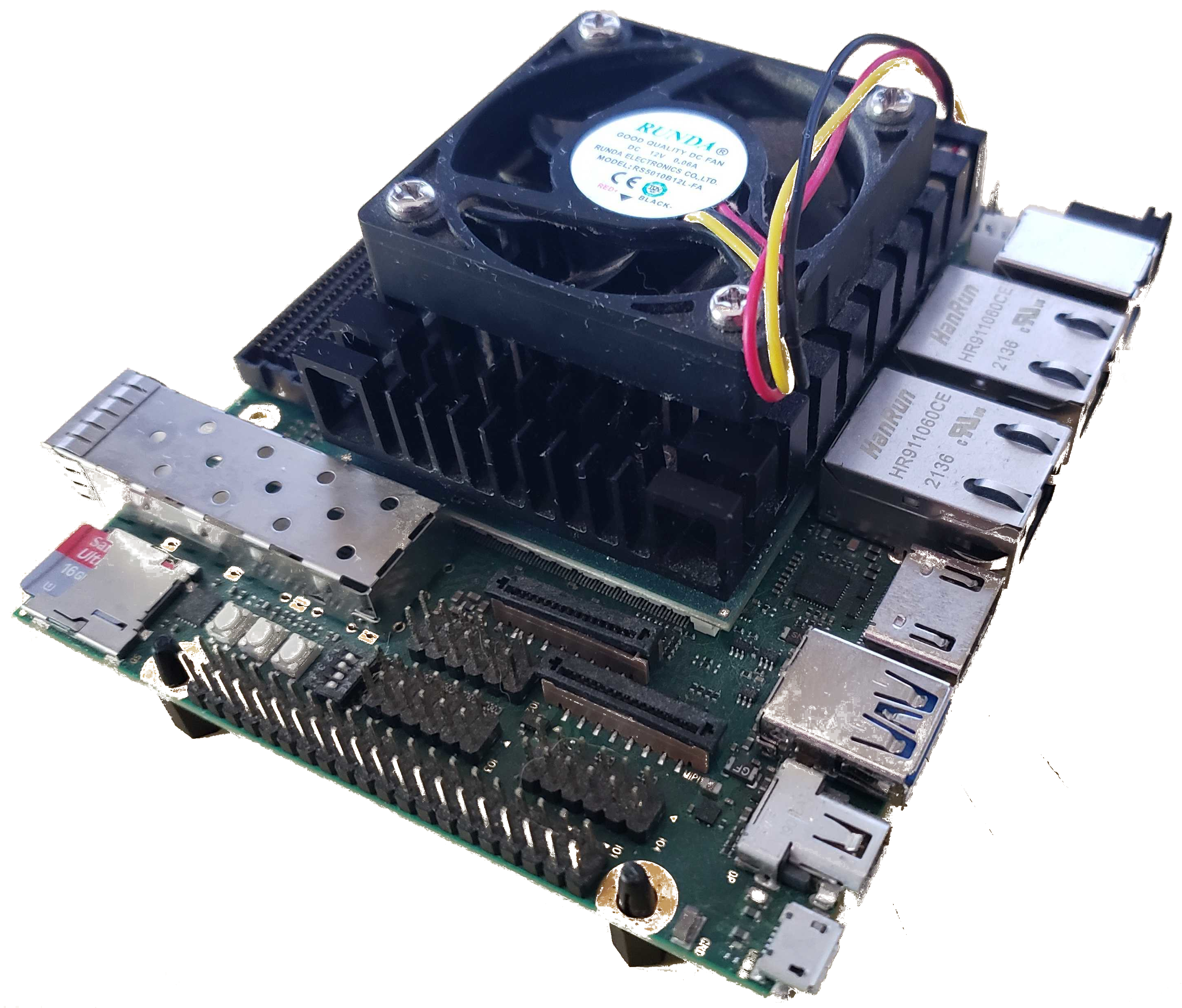 |
I’ll be running my memory tests using my Kimos project. This project uses an Enclustra Mercury+ KX2 carrier board containing a 2GB DDR3 memory and a Kintex-7 160T mounted on an Enclustra Mercury+ ST1 baseboard.
 |
Fig. 5 shows the relevant components of the memory chain used by this Kimos project together with three test points for observation. The project contains a ZipCPU. (Of course!) That ZipCPU has both instruction and data interfaces to memory. Each interface contains a 4kB cache. The instruction cache in particular is large enough to hold all of the instructions required for each of the code loops required by our bench, and so it becomes transparent to the test. This is not true of the data cache. The bench marks I have chosen today are specifically designed to force data cache misses, and then to watch how the controller responds. In the ZipCPU, those two interfaces are then merged together via a Wishbone arbiter, and again merged with a second arbiter with the DMA’s Wishbone requests. The result is that the ZipCPU has only a single bus interface.
Bus requests from the ZipCPU, to include the ZipDMA, are generated at a width designed to match the bus. The interface to the Enclustra’s SDRAM naturally maps to 512 bits, so requests are generated (and recovered) at a 512 bit wide bus width.
Once requests leave the ZipSystem, they enter a crossbar Wishbone interconnect. This interconnect allows the ZipCPU to interact with flash memory, block RAM memory, and the DDR3 SDRAM memory. An additional port also allows interaction with a control bus operating at 32bits. Other peripheral DMAs can also master the bus through this crossbar, to include the SD card controller, an I2C controller, an I2C DMA, and an external debugging bus. Other than loading program memory via the debugging bus to begin the test, these other bus masters will be idle during our testing.
After leaving the crossbar, the Wishbone request goes in one of two directions. It can either go to a Wishbone to AXI converter and then to the MIG, or it can go straight to the UberDDR3 controller. (Only one of these controllers will ever be part of the design at a given time.)
A legitimate question is whether or not the Wishbone to AXI converter will impact this test, or to what extent it will impact it. From a timing standpoint, this converter costs one clock cycle from the Wishbone strobe to the AXI AxVALID signal. This will add one clock of latency to any MIG request. We’ll have to adjust any results we calculate by this one clock cycle. The converter also requires 625 logic elements (LUTs).
What about AXI? The
converter
doesn’t produce full AXI. All requests, coming out of the converter, are
for burst lengths of AxLEN=0 (i.e. one beat), a constant AxID of one bit,
an AxSIZE of 512 bits, AxCACHE=4'd3, and so forth.
-
This will impact area.
A good synthesizer should be able to recognize these constants to reduce both the logic area and logic cost of the MIG. (UberDDR3 is already Wishbone based, so this won’t change anything.)
-
What about AXI bursts?
Frankly, bursts tend to slow down AXI traffic, rather than speed it up. As we’ve already discovered on this blog, the first thing an AXI slave needs to do with a burst request is to unwind the burst. This takes extra logic, and often costs a clock cycle (or two). As a result, Xilinx’s block RAM controller (not the MIG) suffers an extra clock lost on any burst request. The MIG, on the other hand, doesn’t seem affected by burst requests (or lack thereof)–although they may contribute a clock or two to latency.
-
What about AXI pipelining?
Both AXI and the pipelined Wishbone specification I use are pipelined bus implementations. This means that multiple requests may be in flight at a time. I don’t foresee any differences, therefore, between the two controllers due to AXI’s pipelined nature.
Had we been using Wishbone Classic, then our memory performance would’ve taken a significant hit. (This is one of the reasons why I don’t use Wishbone Classic.)
-
What about Read/Write reordering?
The MIG may be able to reorder requests to its advantage. In our test, we will only ever give it a single burst of read or write requests (all with
AxLEN=0), and we will wait for all responses to come back from the controller before switching directions. It is possible that the MIG might have a speed advantage over the UberDDR3 controller in a direction swapping environment. If so, then today’s test is not likely to reveal those differences.
Now that you know something about the various test setups, let’s look at some benchmarks.
The LUT/Size benchmark
When I first started out working with FPGAs, I remember my sorrow at seeing how much of my precious Arty’s LUTs were used by Xilinx’s MIG controller. At the time, I was struggling for funds, and didn’t really have the kind of cash required to purchase a big FPGA with lots of area. An Artix 35T was (roughly) all I could afford, and the MIG used a large percentage of its area.
Since area is proportional to dollars, let’s take a look at how much area each of the controllers uses in today’s test.
On a Kintex-7 160T, mounted on an Enclustra Mercury+ KX2 carrier board, the MIG controller uses 24,833 LUTs out of 101,400 LUTs. This is a full 24.5% of the FPGA’s total logic resources. Fig. 6 shows a Vivado generated hierarchy diagram, showing how much of the design this component requires.
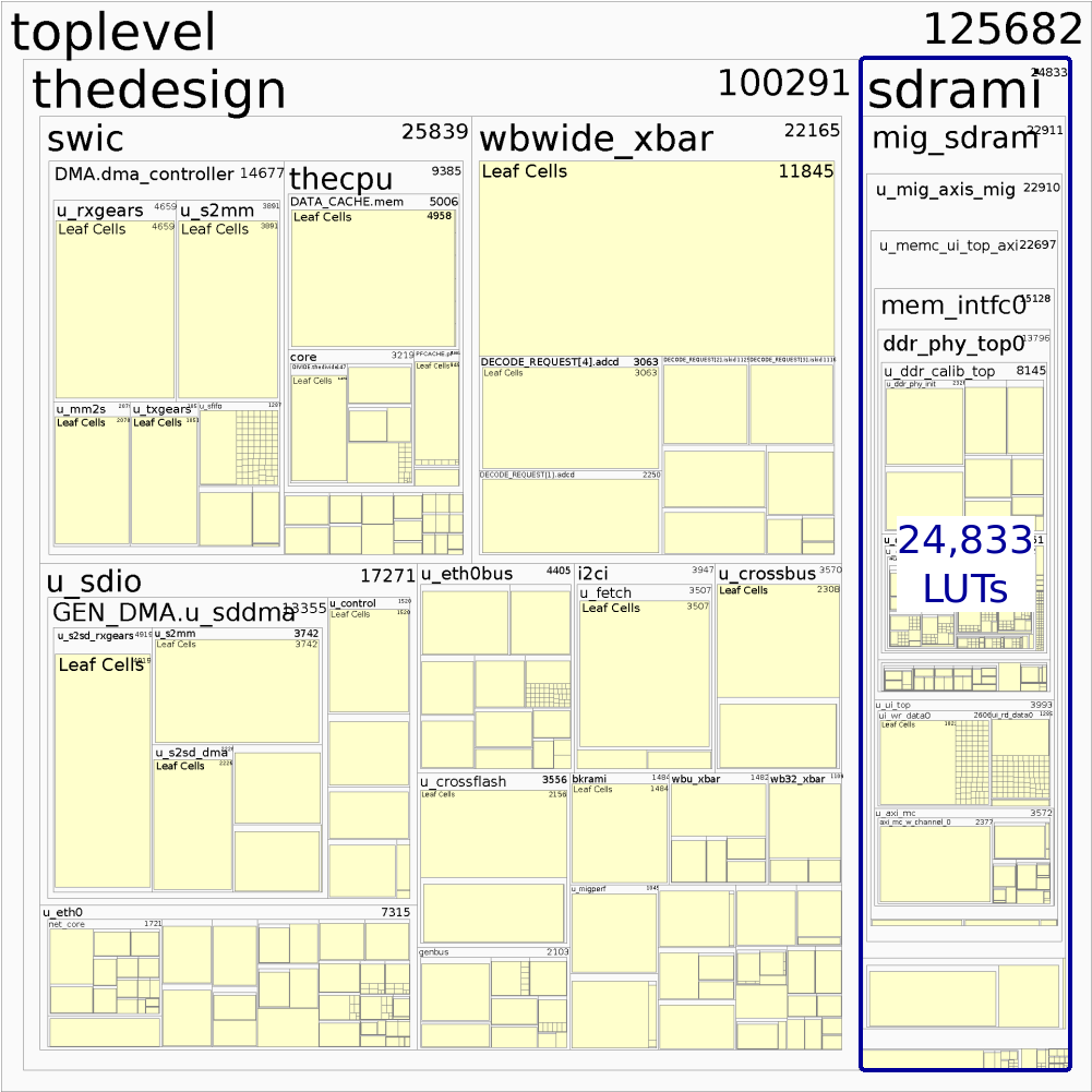 |
The diagram reveals a lot about area. Thankfully, the MIG only uses a quarter of it. The majority of the area used in this design is used by the components that have to touch the 512bit bus. These include the crossbar, the CPU’s DMA, the SDIO controller’s DMA, the various Ethernet bus components, and so on. The most obvious conclusion is that, if you want memory bandwidth, you will have to pay for it. This should come as no surprise to those who have worked in digital design for some time.
On the same board, the UberDDR3 controller uses 13,105 LUTs, or 12.9% of chip’s total logic resources. A similar hierarchy diagram of the design containing the UberDDR3 controller can be found in Fig. 7.
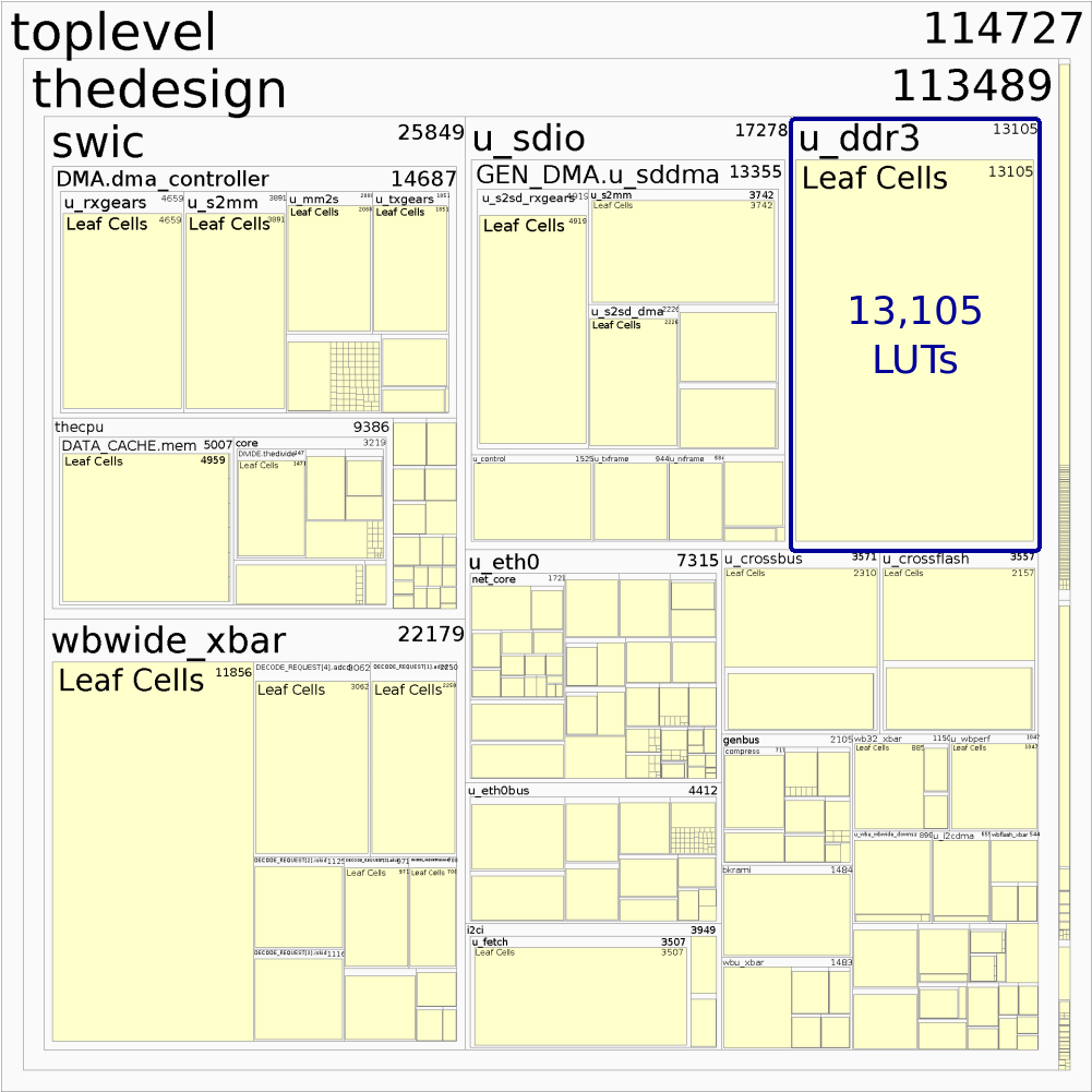 |
To be fair, the Xilinx controller must also decode AXI–a rather complex protocol. However, AXI may be converted to Wishbone for only 1,762 LUTs, suggesting this conversion alone isn’t sufficient to explain the difference in logic cost. Further, the Wishbone to AXI converter used to feed the MIG uses only a restricted subset of the AXI protocol. As a result, it’s reasonable to believe that the synthesizer’s number, 24,833 LUTs, is smaller than what a more complex AXI handler might require.
On size alone, therefore, the UberDDR3 controller comes out as the clear winner.
That makes the UberDDR3 controller cheaper. What about faster?
The raw DMA bench mark
We’ve previously discussed bus benchmarking for AXI. In that article, we identified every type of clock cycle associated with an AXI transaction, and then counted how often each type of cycle took place. Since that article, I’ve built something very similar for Wishbone. In hindsight, however, all of these measures tend to be way too complicated. What I really want is the ability to summarize transactions simply in terms of 1) latency, and 2) throughput. Therefore, I’ve chosen to model all DDR3 transaction times by the equation:
In this model, “Latency” is the time from the first request to the first response, and “Throughput” is the fraction of time you can get one beat returned per clock cycle. Calculating these coefficients requires a basic linear fit, and hence transfers with a varying number of beats used by the DMA–but we’ll get to that in a moment.
The biggest challenge here is that the CPU can very much get in the way of these measures, so we’ll begin our measurements using the DMA alone where accesses are quite simple.
Here’s how the test will work: The CPU will first program the
Wishbone bus measurement
peripheral.
It will then program the DMA to do a memory copy, from DDR3 SDRAM to DDR3
SDRAM. The ZipCPU’s DMA will break
this copy into parts: It will first read N words into a buffer, and then
(as a second step) write those N words to somewhere else on the memory.
During this operation, the CPU will not interact with the DDR3 memory at
all–to keep from corrupting any potential measures. Instead, it will run all
instructions from an on-board block RAM. Once the operation completes, the
CPU will issue a stop collection command to the Wishbone bus measurement
peripheral.
From there, the CPU can read back 1) how many requests were made, 2) how
many clock cycles it took to either read or write each block. From the DMA
configuration, we’ll know how many blocks were read and/or written. From this,
we can create a simple regression to get the latency and throughput numbers we
are looking for.
To see how this might work, let’s start with what a DMA trace might nominally look like. Ideally, we’d want to see something like Fig. 8.
 |
In this “ideal” DMA, the DMA maintains two buffers. If either of the two buffers is empty, it issues a read command. Once the buffer fills, it issues a write command. Fig. 8 shows these read and write requests in the “DMA-STB” line, with “DMA-WE” (write-enable) showing wich direction the requests are being for. These requests then go through a crossbar and hit the DDR3 controller as “SDRAM-STB” and “SDRAM-WE”. (This simplified picture assumes no stalls, but we’ll get to those.) The SDRAM controller might turn around write requests immediately, as soon as they are committed into its queue, whereas read requests will take sometime longer until REFRESH cycles, bank precharging and activation cycles are complete and the data finally returned. Then, as soon as a full block of read data is returned, the DMA can immediately turn around and request to write that data. Once a full block of write data has been sent, the DMA then has the ability to reuse that buffer for the next block of read data.
AXI promises to be able to use memory in this fashion, and indeed my AXI DMA attempts to do exactly that.
When interacting with a real memory, things aren’t quite so simple. Requests will get delayed (I didn’t draw the stall signal in Fig. 8), responses have delays, etc. Further, there is a delay associated with turning the memory bus around from read to write or back again. Still, this is as simple as we can make a bus transaction look.
In Wishbone,
unlike AXI, requests get grouped using the cycle line (CYC).
You can see a notional
Wishbone DMA cycle in
Fig. 9.
 |
Unlike the AXI promise, the ZipCPU’s Wishbone implementation uses only a single buffer, and it doesn’t switch bus direction mid-bus cycle.
Let’s look at this cycle line for a moment through. This is a “feature” not found in AXI. The originating master raises this cycle line on the first request, and drops it after the last acknowledgment. The crossbar uses this signal to know when it can drop arbitration for a given master, to allow a second master to use the same memory. The cycle line can also be used to tell down stream slaves that the originating master is no longer interested in any acknowledgments from its prior requests–effectively acting as a “bus abort” signal. This makes Wishbone more robust than AXI in the presence of hardware failures, but it can also make Wishbone slower than AXI because bursts from different masters cannot be interleaved while the master owning the bus holds its cycle line high.
Arguably, this Wishbone DMA approach will limit our ability to fully test the MIG controller. As a result, we may need to come back to this controller and test again at a later time using an AXI DMA interface alone to see to what extent that might impact our results.
To make our math easier, we’ll add one more requirement: Our transactions will either be to read or write 16, 8, 4, or 2 beats at a time. On a 512bit bus, this corresponds to reading or writing 1024, 512, 256, or 128 bytes at a time–with 1024 bytes being the size of the ZipCPU’s DMA buffer, and therefore the maximum transfer size available.
With all that said, it’s now time to look at some measurement data.
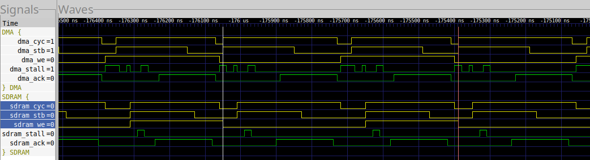
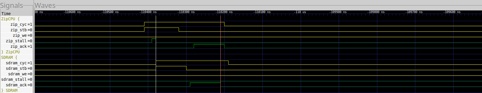
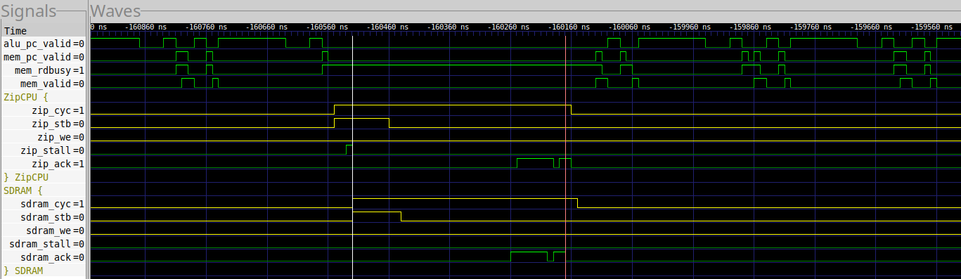
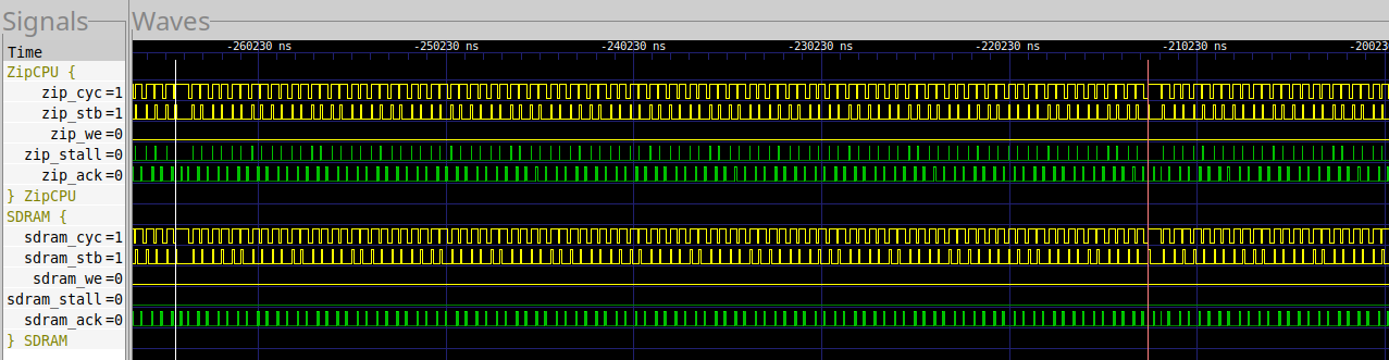
First up is the MIG DDR3 controller. Fig. 10 shows a trace of the DMA waveform when transferring 16 beats of data at a time.
 |
This image shows two Wishbone bus interfaces. The top one is the view the DMA has of the bus. The bottom interface is the view coming out of the crossbar and going into the memory controller.
In this image, it takes a (rough) 79 clock cycles to go from the beginning of one read request, through a write request, to the beginning of the next read request–as measured between the two vertical markers.
Some things to notice include:
- It takes 4 clock cycles for the request to go from the DMA through the crossbar to the controller.
- While not shown here, it takes one more clock cycle following
sdram_stb && !sdram_stallfor the conversion to AXI. - Curiously, the SDRAM STALL line is not universally low during a burst of requests. In this picture, it often rises for a cycle at a time. I have conjectured above that this is due to the MIG’s need for PLL station keeping.
- During writes, it takes 3 clocks to go from request to acknowledgment.
- During reads, it can take 26 clocks from request to acknowledgment–or more.
- Once the MIG starts acknowledging (returning) requests, the ACK line can still drop mid response. (This has cost me no end of heartache!)
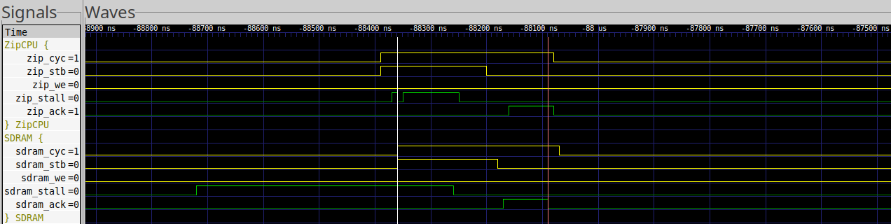
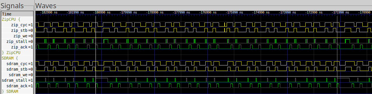
If we repeat the same measurement with the UberDDR3 controller, we get the trace shown in Fig. 11.
 |
In this case, the full 1024 Byte transfer cycle now takes 66 clock cycles instead of 79.
-
It takes 11 cycles from read request to read acknowledgment.
-
It takes 7 cycles from write request to acknowledgment.
-
Unlike the MIG, there’s no periodic loss of acknowledgment. In general, once the acknowledgments start, they continue. This won’t be universally true, but the difference is still significant.
Of course, one transaction never tells the whole story, a full transaction count is required. However, when we look at all transactions, we find on average:
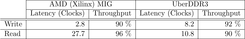 |
These are the clearest performance numbers we will get to compare these two controllers. When writing to memory, the MIG is clearly faster. This is likely due to its ability to turn a request around before acting upon it. (Don’t forget, one of these clocks of latency is due to the Wishbone to AXI conversion, so the MIG is one clock faster than shown in this chart!) Given that the MIG can turn a request around in 1.8 cycles, it must be doing so before examining any of the details of the request!
When reading from memory, the MIG is clearly slower–and that by a massive amount. One clock of this is due to the Wishbone to AXI conversion. Another clock (or two) is likely due to the AXI to native conversion. The MIG must also arbitrate between reads and writes, and must (likely) always activate a row before it can be used. All of this costs time. As a result of these losses and more that aren’t explained by these, the MIG is clearly much slower than the UberDDR3 controller.
Under Load
Now that we’ve seen how the DDR3 controller(s) act in isolation to a DMA, let’s turn our attention to how they act in response to a CPU–the ZipCPU in this case. (Of course!) For our test configuration, the ZipCPU will have both data and instruction caches. Because of this, our test memory loads will need to be extensive–to break through the cache–or else the cache will get in the way of any decent measurement.
How the Cache Works
Let’s discuss the ZipCPU’s data cache for a moment, because it will become important when we try to understand how fast the CPU can operate in various memory environments.
-
First, the ZipCPU has only one interface to the bus. This interface is shared by both the instruction and data caches. However, the instruction cache is (generally) big enough to fit most of our program, so it shouldn’t impact the test much.
The one place where we’ll see the instruction cache impact our test is whenever the ZipCPU needs to cross between cache lines. As currently built, this will cost a one clock delay to look up whether or not the next cache line is in the instruction cache. Other than that, we’re not likely to see any impacts from the instruction cache.
-
The ZipCPU’s data cache is a write through cache. Any attempt to write to memory will go directly to the bus and so to memory. Along the way, the memory in the cache will be updated–but only if the memory to be written is also currently kept in the cache.
-
The ZipCPU will not wait for a write response from memory before going on to its next instruction. Yes, it will wait if the next instruction is a read instruction, but in all other cases the next instruction is allowed to go forward as necessary.
One (unfortunate) consequence of this choice is that any bus error will likely stop the CPU a couple of instructions after the fault, potentially confusing any engineer trying to understand which instruction, which register, and which memory address was associated with the fault. Such faults are often called asynchronous or imprecise bus faults.
-
When issuing multiple consecutive write operations in a row, the ZipCPU will not wait for prior operations to complete. Two of our test cases will exploit this to issue three write (or read) requests in a row. In these tests, the CPU will write either three 32b words or three 8b bytes on consecutive instructions and hence clock cycles.
I tend to call these pipelined writes, and I consider them to be some of the better features of the ZipCPU.
-
All read operations first take a clock cycle to check the cache. As a result, the minimum read time is two cycles: one to read from the cache and check for validity, and a second cycle to shift the 512b bus value and return the 8, 16, or 32b result.
-
As with the write operations, read operations can also be issued back to back. Back to back read operations will have a latency of two clocks, but a 100% throughput–assuming they both read from the same cache line. If not, there will be an additional clock cycle lost to look up whether or not the requested cache line validly exists within the cache.
-
Both instruction and data cache sizes have been set to 4kB each. Both caches will use a line size of eight bus words (512 Bytes). Neither cache uses wrap addressing (although this test will help demonstrate that they should …). Instead, all cache reads will start from the top of the cache line, and the CPU will stall until the entire cache line is completely read before continuing.
To help to understand how this data cache works, let’s examine three operations. The first is a read cache miss, as shown in Fig. 12.
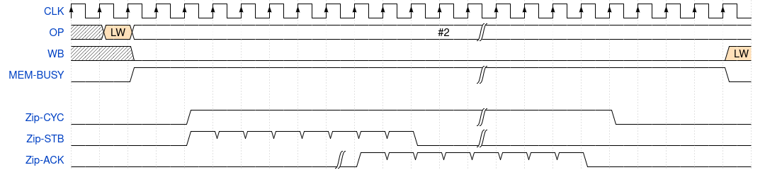 |
In this case, a load word (LW) instruction flows through the
ZipCPU’s pipeline from prefetch (PF),
to decode (DCD), to the read operand (OP)
stage. It then
leaves the read operand (OP) stage headed for the data
cache. The
data cache
requires a couple of clocks–as dictated by the block RAM it’s built from–to
determine
that the request is not in the cache. Once this has been determined, the data
cache initiates
a bus request to read a single cache line (8 bus words) from memory. Both
cycle and strobe lines are raised. The strobe line stays active until eight
cycles of stb && !stall (stall is not shown here, but assumed low). Once
eight requests have been made, the CPU waits for the last of the eight
acknowledgments. Once the read is complete, and not before, the cache line
is declared valid and the CPU can read from it to complete it’s instruction.
This costs another four cycles before the LW instruction can be retired.
While this cache line remains in our cache, further requests to read from memory will take only either two or three clocks: Two clocks if the request is for the same cache line as the prior access, or three clocks otherwise as shown in Fig. 13.
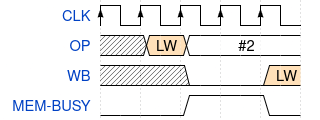 |
Finally, on any write request, the request will go straight to the bus as shown in Fig. 14.
 |
The CPU may then go on to other instructions, but the pipeline will necessarily stall if it ever needs to interact with memory prior to this write operation completing (unless its a set of consecutive writes …).
Sequential LRS Word Access
Our first CPU-based test is that of sequential word access. Specifically, we’ll work our way through memory, and write a pseudo random value to every word in memory–one word at a time. We’ll then come back through memory and read and verify that all of the memory values were written as desired.
From C, the write loop is simple enough:
#define	STEP(F,T)  asm volatile("LSR 1,%0\n\tXOR.C %1,%0" : "+r"(F) : "r"(T))
	// ...
	while(mptr < end) {
		STEP(fill, TAPS);
		// fill = (fill&1)?((fill>>1)^TAPS):(fill>>1);
		*mptr++ = fill;
	}
The “STEP” macro exploits the fact that the ZipCPU’s LSR (logical shift right) instruction shifts the least significant bit into the carry flag, so that an linear feedback shift register (LFSR) may be stepped with only two instructions. The second instruction is a conditionally executed exclusive OR operation, only executed if the carry flag was set–indicating that a one was shifted out of the register.
This simple loop then compiles into the following ZipCPU assembly:
loop:
	LSR        $1,R2	; STEP(fill, TAPS)
	XOR.C      R3,R2
	SW         R2,(R1)	; *mptr = fill
	| ADD        $4,R1	;  mptr++
	CMP        R6,R1	; if (mptr < end)
	BC         loop		;	go to top of loop
Basically, we step the LFSR by shifting right by one. If the bit shifted
over the edge was a one, we exclusive OR the register with our taps. (XOR.C
only performs the exclusive OR if the carry bit is set.)
We then store this word (SW= store word) into our memory address (R1),
increment the address by adding four to it, and then compare the result with
a pointer to the end of our memory region. If we are still less than the
end of memory, we go back and loop again.
Inside the CPU’s pipeline, this loop might look like Fig. 15.
 |
Let’s work our way through the details of this diagram.
-
There are four pipeline stages: prefetch (PF), decode (DCD), read operands (OP), and write-back (WB)
-
The ZipCPU allows some pairs of instructions to be packed together. In this case, I’ve used the vertical bar to indicate instruction pairing. Hence the
S|Ainstruction coming from the prefetch is one of these combined instructions. The instruction decoder turns this into two instructions, forcing the prefetch to stall for a cycle until the second instruction can advance. -
In general and when things are working well, all instructions take one clock cycle. Common exceptions are to this rule are made for memory, divide, and multiply instructions. For this exercise, only memory operations will take longer.
-
The store word instruction must stall and wait if the memory unit is busy. For the example in Fig. 15, I’ve chosen to begin the example with a busy memory, so you can see what this might look like.
-
Once the store word request has been issued to the memory controller, a bus request starts and the CPU continues with its next instruction.
-
The bus request must go through the crossbar to get to the SDRAM. As shown here, this takes three cycles.
-
The memory then accepts the request, and acknowledges it.
In the case of the MIG, this request is acknowledged almost immediately. The UberDDR3 controller takes several more clock cycles before acknowledging this request.
-
It takes another clock for this acknowledgment to return back through the crossbar to the CPU.
-
By this time, the CPU has already gone ahead without waiting for the bus return. However, once returned, the CPU can accept a new memory instruction request.
-
When the ZipCPU hits the branch instruction (
BC= Branch if carry is set), the CPU must clear its pipeline to take the branch. This forces the pipeline to be flushed. The colorless instructions in Fig. 15 are voided, and so never executed. The jump flag is sent to the prefetch and so the CPU must wait for the next instruction to be valid. (No, the ZipCPU does not have any branch prediction logic. A branch predictor might have saved us from these stalls.) If, as shown here, the branch remains in the same instruction cache line, a new instruction may be returned immediately. Otherwise it may take another cycle to complete the cache lookup for an arbitrary cache line.
If you look closely, you’ll notice that the performance of this tight loop is heavily dependent upon the memory performance. If the memory write cannot complete by the time the next write needs to take place, the CPU must then stall and wait.
Using our two test points, we can see how the two controllers handle this test. Of the two, the MIG controller is clearly the fastest, although the speed difference is (in this case) irrelevant.
 |
Indeed, as we’ve discussed, the MIG’s return comes back so fast that it is clear the MIG has not completed sending this request to the DDR3. Instead, it’s just committed the request to its queue, and then returns its acknowledgment. This acknowledgment also comes back fast enough that the CPU memory controller is idle for two cycles per loop. As a result, the memory write time is faster than the loop, and the loop time (10 clock cycles, from marker to marker) is dominated by the time to execute each of the instructions.
Let’s now look at the trace from the UberDDR3 controller shown in Fig. 17.
 |
The big thing to notice here is that the UberDDR3 controller takes one more clock cycle to return a busy status. Although this is slower than the MIG, it isn’t enough to slow down the CPU, so the loop continues to take 10 cycles per loop.
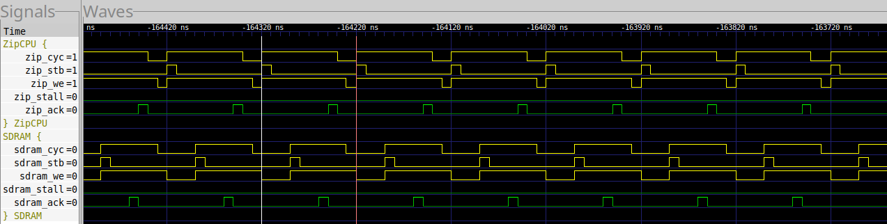
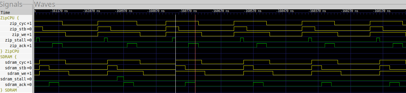
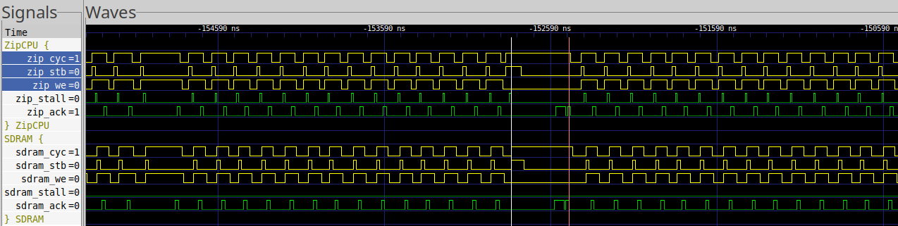
If you dig just a bit deeper, you’ll find that every 22us or so, the MIG takes longer to acknowledge a write request.
 |
In this case, the loop requires 22 clock cycles to complete.
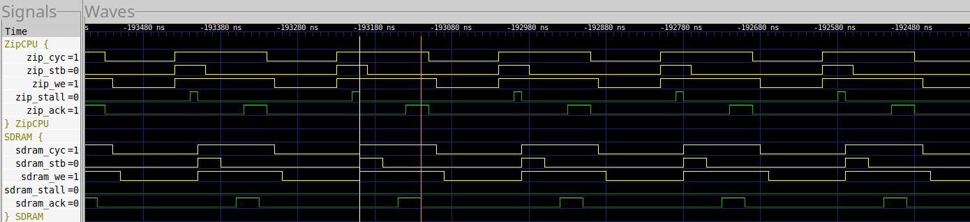
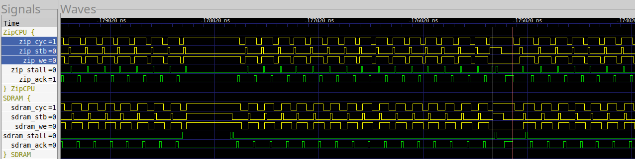
In a similar fashion, every 827 clocks (8.27 us), the UberDDR3 controller does a memory refresh. During this time, the UberDDR3 controller will also take longer to acknowledge a write request.
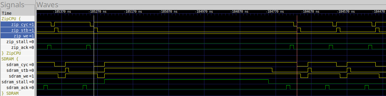 |
In this case, it takes the UberDDR3 controller 57 clocks to complete a single loop.
Let’s now turn our attention to the read half of this test, where we go back through memory in roughly the same fashion to verify the memory writes completed as desired. In particular, we’ll want to look at cache misses. Such misses don’t happen often, but they are the only time the design interacts with its memory.
From C, our read loop is similarly simple:
#define	FAIL		asm("TRAP")
	// ...
	while(mptr < end) {
		STEP(fill, TAPS);
		if (*mptr != (int)fill)
			FAIL;
		mptr++;
	}
The big difference here is that, if the memory every fails to match the pseudorandom sequence, we’ll issue a TRAP instruction which will cause the CPU to halt. This forces a branch into the middle of our loop.
loop:
	LSR        $1,R0	; STEP(fill, TAPS)
	XOR.C      R2,R0
	LW         (R1),R3	; *mptr
	| CMP      R0,R3
	BZ         no_trap	; if (*mptr == (int)fill) ... skip
	TRAP			;   break into supervisor mode--never happens
no_trap:
	ADD        $4,R1	; mptr++
	| CMP      R6,R1	; if (mptr < end)
	BC         loop		;   loop some more
Inside the CPU’s pipeline, this loop might look like Fig. 20.
 |
This figure shows two times through the loop–one with a cache miss, and one where the data fits entirely within the cache. In this case, the time through the loop upon a cache miss is entirely dependent upon how long the memory controller takes to read. EVERY clock cycle associated with reading from memory (on a cache miss) costs us.
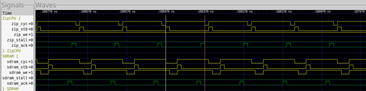
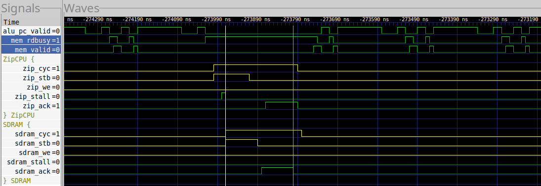
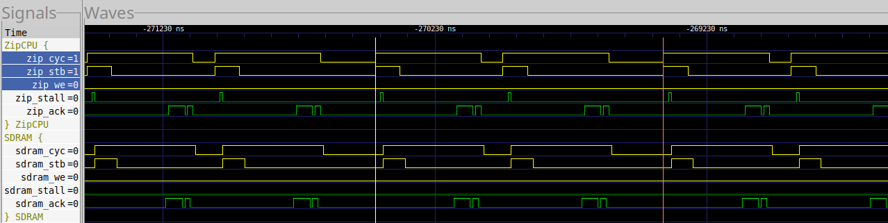
Fig. 21 shows a trace captured from the MIG during this operation.
 |
Here we can see that it takes 35 cycles to read from memory on a cache miss. These 35 cycles directly impact that time it takes to complete our loop.
Since the memory is being read into the data cache, we are reading eight 512 bit words at a time, which we will then process 32 bits per loop. Hence, one might expect a cache miss one of every 128 loops.
Accepting that it takes us 17 clocks to execute this loop without a cache miss, we can calculate the loop time with cache misses as:
 |
In this case, the probability of a cache miss is once every 128 times through. The other latency is 4 clocks for the crossbar, and another 5 clocks in the cache controller. Hence, our loop time for a 35 cycle read, one every 128 times, is about 17.5 cycles. This is pretty close to the measured time of 17.35 cycles.
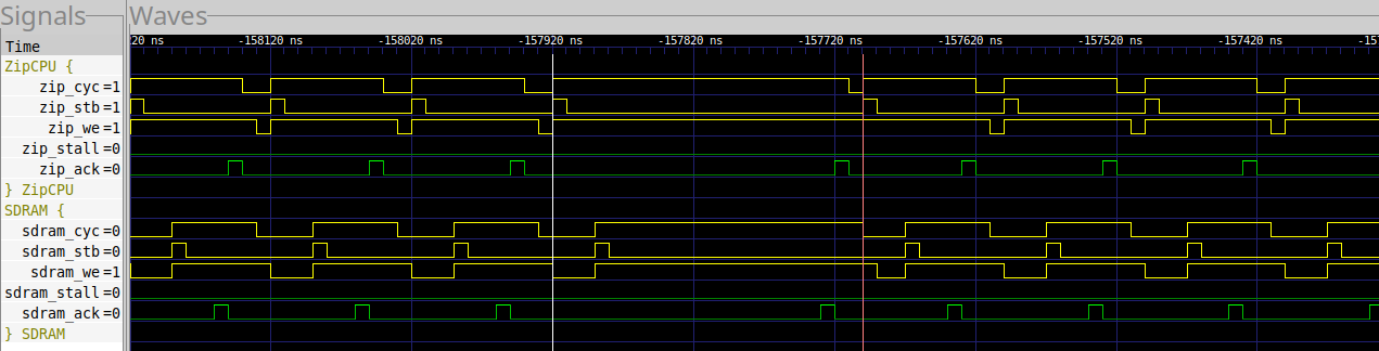
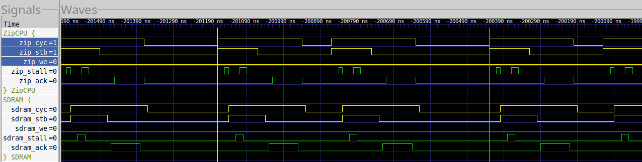
How about the UberDDR3 controller? Fig. 22 shows us an example waveform.
 |
In this case, it takes 17 clock cycles to access the DDR3 SDRAM. From this one might expect 17.07 clocks per loop. In reality, we only get about 17.23, likely due to the times when our reads land on REFRESH cycles, as shown in Fig. 23 below, where the read takes 27 clocks instead of 17.
 |
Our conclusion? In this test case, the differences between the MIG and UberDDR3 controllers are nearly irrelevant. The MIG is faster for singleton writes, but we aren’t writing often enough to notice. The UberDDR3 controller is much faster when reading, but the cache helps to hide the difference.
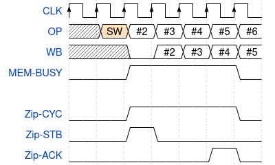
Sequential LRS Triplet Word Access
Let’s try a different test. In this case, let’s write three words at a time, per loop, and then read them back again. As before, we’ll move sequentially through memory from one end to the next. Our goal will be to exploit the ZipCPU’s pipelined memory access capability, to see to what extent that might make a difference.
Why are we writing three values to memory? For a couple reasons. First, it can be a challenge to find enough spare registers to write much more. Technically we might be able to write eight at a time, but we still need to keep track of the various pointers and so forth for the rest of the function we’re using. Second, three is an odd prime number. This will force us to have memory steps that cross cache lines, making for some unusual accesses.
Here’s the C code for writing three pseudorandom words to memory.
	while(mptr+3 < end) {
		register unsigned a, b, c;

		STEP(fill, TAPS);	a = fill;
		STEP(fill, TAPS);	b = fill;
		STEP(fill, TAPS);	c = fill;

		mptr[0] = a;
		mptr[1] = b;
		mptr[2] = c;

		mptr += 3;
	}
As before, we’re using the STEP macro (defined above) to step a linear
feedback shift register, used as a pseudorandom number generator, and then
writing these pseudorandom numbers to memory. As before, the pseudo in
pseudorandom will be very important when we try to verify that our memory
was written correctly as intended.
GCC converts this C into the following assembly. (Note, I’ve renamed the Loop labels and added comments, etc., to help keep this readable.)
loop:
	MOV        R3,R2	; STEP(fill, TAPS); a = fill;
	LSR        $1,R2
 	XOR.C      R8,R2
	MOV        R2,R4	; STEP(fill, TAPS); b = fill;
	LSR        $1,R4
	XOR.C      R8,R4
	MOV        R4,R3	; STEP(fill, TAPS); c = fill;
	LSR        $1,R3
	XOR.C      R8,R3
	SW         R2,$-12(R0)	; mptr[0] = a;
	SW         R4,$-8(R0)	; mptr[1] = b;
	SW         R3,$-4(R0)	; mptr[2] = c;
	| ADD      $12,R0	; mptr += 3;
	CMP        R6,R0	; if (mptr+3 < end)
	BC         loop
Even though we’re operating on three words at a time, the loop remains quite
similar. LSR/XOR.C steps the LRS. Once we have three values, we use
three consecutive SW (store word) instructions to write these values to
memory. We then adjust our pointer, compare, and loop if we’re not done yet.
Fig. 24 shows what the CPU pipeline might look like for this loop.
 |
Unlike our first test, we’re now crossing between instruction cache lines.
This means that there’s a dead cycle between the LSR and XOR instructions,
and another one following the BC (branch if carry) loop instruction before
the prefetch is able to return the first instruction.
Unlike the last test, our memory operation takes three consecutive cycles.
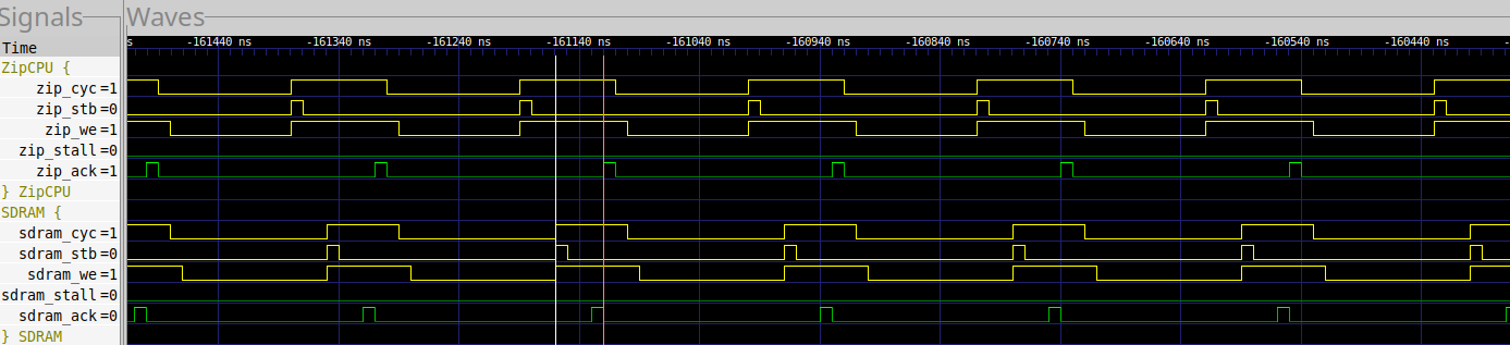
Here’s a trace showing this write from the perspective of the MIG controller.
 |
In this case, it takes 6 clocks (as shown) for the MIG to acknowledge all three writes. You’ll also note that the crossbar stalls the requests, but that you don’t see any evidence of that at the SDRAM controller. This is simply due to the fact that it takes the crossbar a clock to arbitrate, and it has a two pipeline stage buffer before arbitration is required. As a result, the third request through this crossbar routinely stalls. Put together, this entire loop requires 21 cycles from one request to the next.
Now let’s look at a trace from the UberDDR3 controller.
 |
In this case, it takes 8 clocks for 3 writes. The UberDDR3 controller is two clocks slower than the MIG. However, it still takes 21 cycles from one request to the next, suggesting that we are still managing to hide the memory access cost by running other instructions in the loop. Indeed, if you dig just a touch deeper, you’ll see that the CPU has 9 spare clock cycles. Hence, this write could take as long as 17 cycles before it would impact the loop time.
Let’s now turn our attention to reading these values back. As before, we’re going to read three values, and then step and compare against our three pseudorandom values.
	while(mptr+3 < end) {
		register unsigned a, b, c;

		a = mptr[0];
		b = mptr[1];
		c = mptr[2];

		STEP(fill, TAPS);
		if (a != (int)fill) {
			FAIL; break;
		}

		STEP(fill, TAPS);
		if (b != (int)fill) {
			FAIL; break;
		}

		STEP(fill, TAPS);
		if (c != (int)fill) {
			FAIL; break;
		}

		mptr+=3;
	}
Curiously, GCC broke our three requests up into a set of two, followed by a separate third request. This will break the ZipCPU’s pipelined memory access into two accesses, although this is still within what “acceptable” assembly might look like.
loop:
	ADD        $12,R2       ; mptr += 3
	| CMP      R6,R2	; while(mptr+3 < end)
	BNC        end_of_loop
	LW         -8(R2),R4	; b = mptr[1]
	LW         -4(R2),R0	; c = mptr[2]
	LSR        $1,R1	; STEP(fill, TAPS);
	XOR.C      R3,R1
	LW         -12(R2),R11	; a = mptr[0]
	CMP        R1,R11	; if (a != (int)fill)
	BNZ        trap
	LSR        $1,R1	; STEP(fill, TAPS);
	XOR.C      R3,R1
	CMP        R1,R4	; if (b != (int)fill)
	BNZ        trap
	LSR        $1,R1	; STEP(fill, TAPS);
	XOR.C      R3,R1
	CMP        R1,R0	; if (c == (int)fill)
	BZ         loop		;	go back and loop again
trap:
One lesson learned is that the if statements should include not only the TRAP/FAIL instruction, but also a break instruction. If you include the break, then GCC will place the TRAP outside of the loop and so we’ll no longer have to worry about multiple branches clearing our pipeline per loop. If you don’t, then the CPU will have to deal with multiple pipeline stalls. Instead, we’ll have only one stall when we go around the loop.
From a pipeline standpoint, the pipeline will look like Fig. 27.
 |
In this figure, we show two passes through the loop. The first pass shows a complete cache miss and subsequent memory access, whereas the second one can exploit the fact that the data is in the cache.
As before, in the case of a cache miss, the loop time will be dominated by the memory read time. Any delay in memory reading will slow our loop down directly and immediately, but only once per cache miss. The difference here is that our probability of a cache miss has now gone from one in 128 to three in 128.
On a good day, the MIG’s access time looks like Fig. 28 below.
 |
In this case, it costs us 35 clocks to read from the SDRAM in the case of a cache miss, and 24 clocks with no miss. Were this always the case, we might expect 25 clocks per loop. Instead, we see an average of 27 clocks per loop, suggesting that the refresh and other cycles are slowing us down further.
Likewise, a cache miss when using the UberDDR3 controller looks like Fig. 29.
 |
In this case, it typically costs 17 clocks on a cache miss. On a rare occasion, the read might hit a REFRESH cycle, where it might cost 36 clocks or so. Hence we might expect 24.6 cycles through the loop, which is very close to the 24.7 cycles measured.
Sequential LRS Triplet Character Access
The third CPU test I designed is a repeat of the last one, save that the CPU made character (i.e. 8-bit octet) accesses instead of 32-bit word accesses.
In hind sight, this test isn’t very revealing. The statistics are roughly the same as the triplet word access: memory accesses to a given row aren’t faster (or slower) when accessing 8-bits at a time instead of 32. Instead, three 8-bit accesses takes just as much time as three 32-bit access. The only real difference here is that the probability of a read cache miss is now 3 bytes in a 512 cache line, rather than the previous 3 in 128.
Random word access
A more interesting test is the random word access test. In this case, we’re going to generate both (pseudo)random data and a (pseudo)random address. We’ll then store our random data at the random address, and only stop once the random address sequence repeats.
I’m expecting a couple differences here. First, I’m expecting that almost all of the data cache accesses will go directly to memory. There should be no (or at least very few) cache hits. Second, I’m going to expect that almost all of the memory requests should require loading a new row. In this case, the MIG controller should have a bit of an advantage, since it will automatically precharge a row as soon as it recognizes its not being used.
Writing to memory from C will look simple enough:
	afill = initial_afill;
	do {
		STEP(afill, TAPS);
		STEP(dfill, TAPS);
		if ((afill&(~amsk)) == 0)
			mptr[afill&amsk] = dfill;
	} while(afill != initial_afill);
GCC then turns this into the following assembly.
loop:
	LSR        $1,R1	; STEP(afill, TAPS)
	XOR.C      R8,R1
	LSR        $1,R2	; STEP(dfill, TAPS)
	XOR.C      R8,R2
	MOV        R1,R3        ; if (afill & (~amsk)) == 0
	| AND      R12,R3
	BNZ        checkloop
	; Calculate the memory address
	MOV        R11,R3        | AND        R1,R3
	LSL        $2,R3
	MOV        R5,R9         | ADD        R3,R9
	SW         R2,(R9)	; mptr[afill & amsk] = dfill
checkloop:
	CMP        R1,R4
	BNZ        loop
There’s a couple of issues here in this test. First, we have a mid-loop
branch that we will sometimes take, and sometimes not. Second, we now have
to calculate an address. This requires multiplying the pseudorandom
values by four (LSL 2,R3), and adding it to the base memory address.
I’ve drawn out a notional pipeline for what this might look like in Fig. 30.
 |
Notice that this notional pipeline includes a stall for crossing instruction
cache line boundaries between the XOR and LSR instructions.
From the MIG’s standpoint, a typical random write capture looks like Fig. 31 below.
 |
As before, this is a 4 clock access. The MIG is simply returning it’s results before actually performing the write.
A similar trace, drawn from the UberDDR3 controller can be seen in Fig. 32.
 |
In this case, it takes 8 clocks to access memory and perform the write.
However, neither write time is sufficient to significantly impact our time through the loop. Instead, it’s the rare REFRESH cycles that impact the write, but again these impacts are only fractions of a clock per loop. Still, that means that the UberDDR3 controller takes seven tenths of a cycle longer per loop than the MIG controller.
Reads, on the other hand, are more interesting. Why? Because read instructions must wait for their result before executing the next instruction, and the cache will have a negative effect if we’re always suffering from cache misses.
Here’s the C code for a read. Note that we now have two branches, mid loop.
	do {
		STEP(afill, TAPS);
		STEP(dfill, TAPS);
		if ((afill & (~amsk)) == 0) {
			if (mptr[afill&amsk] != (int)dfill) {
				FAIL;
				break;
			}
		}
	} while(afill != initial_afill);
GCC produces the following assembly for us.
loop:
	LSR        $1,R2	; STEP(afill, TAPS)
	XOR.C      R4,R2
	LSR        $1,R0	; STEP(dfill, TAPS)
	XOR.C      R4,R0
	MOV        R2,R3
	| AND      R12,R3
	BNZ        skip_data_check
	MOV        R11,R3	; Calculate afill & amsk
	| AND      R2,R3
	LSL        $2,R3	; Turn this into an address offset
	MOV        R5,R1
	| ADD      R3,R1	; ... and add that to mptr
	LW         (R1),R3	; Read mptr[afill&amsk]
	| CMP      R0,R3	; Compare with dfill, the expected data
	BNZ        trap		; Jump to the FAIL/break if nonzero
skip_data_check:
	LW         12(SP),R1	; Load (from the stack) the initial address
	| CMP      R2,R1	; Check our loop condition
	BNZ        loop
	// ...
trap:
There’s a couple of things to note here. First, there’s not one but two
memory operations here. Why? GCC couldn’t find enough registers to hold
all of our values, and so it spilled the initial address onto the stack.
Nominally, this wouldn’t be an issue. However, it becomes an issue when
you have a data cache collision, where both the stack and the SDRAM memory
require access to the same cache line. These cases then require two cache
lookups per loop. One lookup will be of SDRAM, the other (LW 12(SP),R1)
of block RAM where the stack is being kept. (A 2-way or higher data cache
may well have mitigated this effect, allowing the stack to stay in the cache
longer.)
Second, notice how we now have a BNZ (branch if not zero, or if not equal).
This is what we get for adding the break instruction to our failure part of
the loop–letting GCC know that this if condition isn’t really part of our
loop. As a result, we only have one branch–and that only if our pseudorandom
address goes out of bounds.
This leaves us with a pipeline looking like Fig. 33.
 |
A capture of these random reads, when using the MIG controller, looks like Fig. 34 below.
 |
As before, we’re looking at 35 clocks to read 8 words. Nominally, we might argue this to be a latency of 27 cycles plus overhead, but … it’s not. One cycle, after the MIG starts returning data, is empty. This means we have a latency of 26 cycles, and a single clock loss of throughput on every transaction.
Judging from the UberDDR3 controller trace in Fig. 35, the UberDDR3 controller doesn’t have this problem.
 |
Instead, it takes 17 clocks to access 8 words, and there’s no unexpected losses in the return.
As a result, the MIG controller requires 72 clocks per loop, whereas the UberDDR3 controller requires 55 clocks per loop.
My conclusion from this test is that the MIG remains faster when writing, but the difference is fairly irrelevant because the CPU continues executing instructions concurrently. In the case of reads, on the other hand, the UberDDR3 controller is much faster. This is the conclusion one might expect given that the UberDDR3 controller has much less latency than the MIG.
MEMCPY
Let’s now leave our contrived tests, and look at some C library functions. For reference, the ZipCPU uses the NewLib C library.
Our first test will be a memcpy() test. Specifically, we’ll copy the first half of our memory to the second half. This will maximize the size of the memory copied.
In addition, our memcpy() requests will be aligned. This will allow the library routine to use 32b word copies instead of byte copies. It’s faster and simpler, but there is some required magic taking place in the library to get to this point.
Our test choice also has an unexpected consequence. Specifically, the UberDDR3’s sequential memory optimizations will all break at the bank level, since we’ll be reading from one bank, and writing to another address on the same bank. This will force the UberDDR3 controller to precharge a row and activate another on every bank read access. (It’s not quite every access, since we do have the data cache.)
With a little digging, the relevant loop within the memcpy() compiles into the following assembly:
loop:
	LW         (R5),R8	; Load two words from memory
	LW         4(R5),R9
	SW         R8,(R4)	; Store them
	SW         R9,$4(R4)
	LW         8(R5),R8	; Load the next two words
	LW         12(R5),R9
	SW         R8,$8(R4)	; Store those as well
	SW         R9,$12(R4)
	LW         16(R5),R8	; Load a third set of words
	LW         20(R5),R9
	SW         R8,$16(R4)	; Store the third set
	SW         R9,$20(R4)
	ADD        $32,R5        | ADD        $32,R4
	LW         -8(R5),R8	; Load a final 4th set of words
	LW         -4(R5),R9
	SW         R8,$-8(R4)	; ... and store them to memory
	SW         R9,$-4(R4)    | CMP        R4,R6
	BNZ        loop
Note that all of the memory accesses are for two sequential words at a time. This is due to the fact that both GCC and memcpy() believe the ZipCPU has native 64-bit instructions. It doesn’t, but this is still a decent optimization.
Second, note that GCC and NewLib have succeeded in unrolling this loop, so that four 64b words are read and written per loop. (I’m not sure which of GCC or NewLib is responsible for this optimization, but it shouldn’t be too hard to look it up.)
Third, note that the load-word instructions cannot start until the store-word instructions prior complete. This is to keep the CPU from hitting certain memory access collisions.
Fig. 36 shows an example of how the MIG deals with this memory copy.
 |
Highlighted in the trace is the 35 cycle read.
However, you’ll also note that this trace is primarily dominated by write requests. This is due to the fact that the ZipCPU has a write-through cache, so all writes go to the data bus–two words at a time. Because of the latency difference we’ve seen, these writes can complete in 5 cycles total, or 14 cycles from one write to the next.
Remember, the read requests cannot be issued until the write requests
can complete. Hence, for any pair of SW (store word) instructions followed
by LW (load word) instructions, the LW instructions must wait for the
SW instructions to complete. This write latency directly impacts that
wait time. Hence, it takes 14 cycles from one write to the next.
Also shown in Fig. 36 is a write when the SDRAM was busy. These happen periodically, when the MIG takes the SDRAM offline–most likely to refresh some of its capacitors. These cycles, while rare, tend to cost 71 clock cycles to write two words.
In the end, it took 55 cycles to read and write 8 words (32 bytes) when the read data was in the cache, or 87 cycles otherwise.
Fig. 37, on the other hand, shows a trace of the same only this time using the UberDDR3 controller.
 |
As before, reads are faster. The UberDDR3 controller can fill a cache line in 17 cycles, vs 35 for the MIG controller.
However, what kills the UberDDR3 controller in this test is its write performance. Because of the higher latency requirement of the write controller, it typically takes 7 cycles for a two word write to complete. This pushes the two word time from 14 cycles to 16 cycles. As a result, the UberDDR3 controller is 15% slower than the MIG in this test.
MEMCMP
Our final benchmark will be a memory comparison, using memcmp(). Since we just copied the lower half of our memory to the upper half using memcpy() in our last test, we’re now set up for a second test where we verify that the memory was properly copied.
Our C code is very simple.
	if (0 != memcmp(mem+lnw/2, mem, lnw/2))
		FAIL;
Everything taking place, however, lands within the memcmp() library call.
Internally, we spend our time operating on the following loop over and over again:
loop:
	LW         (R1),R4	; Read two words from the left hand side
	LW         4(R1),R5
	LW         (R2),R6	; Read two words from the right hand side
	LW         4(R2),R7
	CMP        R6,R4	; Compare left and right hand words
	CMP.Z      R7,R5
	BNZ        found_difference
	ADD        $8,R1         | ADD        $8,R2	; Increment PTRs
	ADD        $-8,R3        | CMP        $8,R3	; End-of-Loop chk
	BNC        loop
As with memcpy(), the library is try to exploit the 64b values that the ZipCPU supports–albeit not natively. Hence, each 64b read is turned into two adjacent reads, and the comparison is likewise turned into a pair of comparisons, where the second comparison is only accomplished if the first comparison is zero. On any difference, memcmp() breaks out of the loop and traps. Things are working well, however, so there are no differences, and so the CPU stays within the loop until it finishes.
Also, like the memcpy() test, jumping across a large power of two divide will likely break the bank machine optimizations used by the UberDDR3 controller.
Enough predictions, let’s see some results.
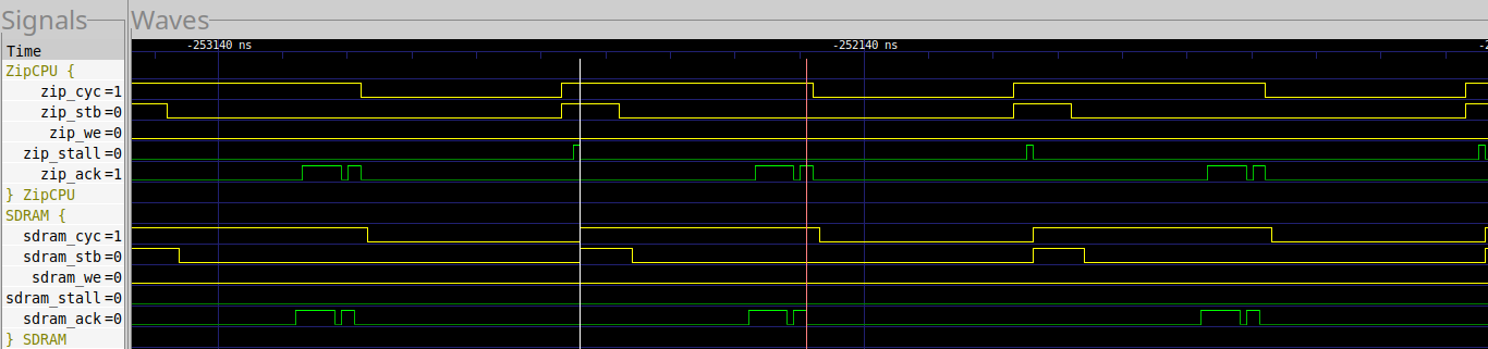
Fig. 38 shows an example loop through the MIG Controller.
 |
One loop, measured between the markers, takes 106 clocks.
Much to my surprise, when I dug into this test I discovered that every memory access resulted in a cache miss. The reason is simple: the two memories are separated by a power of two amount, yet greater than the cache line size. This means that the two pieces of memory, the “left hand” and “right hand” sides, both use the same cache tags. Therefore, they are both competing for the same cache line. (A 2-way cache may have mitigated this reality, but the ZipCPU currently has only one-way caches.)
Fig. 39 shows the comparable loop when using the UberDDR3 controller.
 |
In this case, the memcmp() uses only 74 clocks per loop–much less than the 106 used by the MIG..
Something else to note is that if you zoom out from the trace in Fig. 38, you can see the MIG’s refresh cycles. Specifically, every 51.8us, there’s a noticable hiccup in the reads, as shown in Fig. 40.
 |
The same refresh cycles are just as easy to see, if not easier, in the UberDDR3 controller’s trace if you zoom out, as shown in Fig. 41.
 |
This might explain why the MIG gets 96% throughput, whereas the UberDDR3 controller only gets a rough 90% throughput: the MIG doesn’t refresh nearly as often.
Still, when you put these numbers together, overall the UberDDR3 controller is 30% faster than the MIG when running the MEMCMP test.
Conclusions
So what conclusion can we draw? Is the UberDDR3 controller faster, better, and cheaper than the MIG controller? Or would it make more sense to stick with the MIG?
As with almost all engineering, the answer is: it depends.
-
The UberDDR3 controller is clearly cheaper than the MIG controller, since it uses 48% lower area.
-
Reading is much faster when using the UberDDR3 controller, primarily due to its lower latency of 10.8 clocks vice the MIGs 27.7 clocks (on avererage). This lower latency is only partially explained by the MIG’s need to process and decompose AXI bursts. It’s not clear what the rest of latency is caused by, or why it ends up so slow.
At the same time, this read performance improvement can often be hidden by a good cache implementation. This only works, though, when accessing memory from a CPU. Other types of memory access, such as DMA reading or video framebuffer reading won’t likely have the luxury of hiding the memory performance, since they tend to read large consecutive areas of memory at once, rather than accessing random memory locations.
-
Writing is faster when using the MIG, primarily due to the fact that it acknowledges any write request (nearly) immediately.
This should be an easy issue to fix.
-
The UberDDR3 controller might increase its throughput to match the MIG, were it to use a different refresh schedule.
I would certainly recommend Angelo look into this.
-
I really need to implement WRAP addressing for my data cache. I might’ve done so for this article, once I realized how valuable it would be, but then I realized I’d need to go and re-collect all of the data samples I had, and re-draw all of the pipeline diagrams. Instead, I’ll just push this article out first and then take another look at it.
-
The memcmp() test also makes a strong argument for having at least a 2-way cache implementation.
Given that the UberDDR3 controller is still somewhat new, I think we can all expect more and better things from it as it matures.
For he looketh to the ends of the earth, and seeth under the whole heaven; to make the weight for the winds; and he weigheth the waters by measure. Job 28:24-25