
Building a high speed Finite Impulse Response (FIR) Digital Filter
Some time ago, an individual posted on Digilent’s forum that he wasn’t able to get Xilinx’s Finite Impulse Response (FIR) filter compiler generated code to work. While I can understand that there are good reasons for using a FIR compiler, this individual was attempting to low-pass filter a signal with less than a handful of taps.
No wonder why he was getting frustrated when he didn’t see much difference in the filtered signal.
He’s not alone. Indeed, I was answering forum posts from a similar individual on another forum just this morning. It seems like requests for help with the vendor supplied digital filtering libraries are fairly common place, while many of those asking for help don’t necessarily understand what goes on within a typical digital filter.
If you would like to apply a digital filter to a signal, I am going to suggest that you should first learn what a digital filter is. I’m also going to suggest that you learn how the frequency response of a filter is defined, to the point where you can calculate the frequency response yourself and so know what to expect from your any digital filter implementation.
When you think you are ready to learn how to implement a digital filter, then let me welcome you to continue reading.
Today, let’s look at what’s required to implement an FIR digital filter.
Uses for Digital Filters
Years ago I asked a math professor why I should be interested in Linear Algebra. He was rather flabbergasted and floored by the question. Linear Algebra, he tried to explain, underpinned so much of mathematics that it was hard to define just one use.
The same is true of digital filtering–which just so happens to be one of those many uses of Linear Algebra that my instructor didn’t reference. Digital filters are used in so many Digital Signal Processing (DSP) applications within digital logic, such as FPGAs, that it’s hard to identify just one application to use when arguing for their relevance.
The following, though, are some common uses of the sorts of digital filters you can create within an FPGA:
-
Audio pre/post emphasis, often used in commercial audio transmission channels
-
Channel separation and selection, such as your radio receiver might do.
-
Echo cancellation in telephony
-
Audio equalization, such as you might find on any higher quality stereo set
-
Matched Filtering to maximize SNR, often used within digital communications
-
Intersymbol Interference mitigation in digital communications
-
Anti-aliasing filters, so that you can process your signals at a slower rate without distortion
-
In hearing aids, to clean up audio signals so that they may be understood again
Indeed, as I’m putting this list together, I feel like I’ve only started to touch the surface on the uses of digital filters. Their usage has become quite ubiquitous, even if they are not well understood by all who design and use them.
Today, let’s build some generic filter logic that can be used for any or all of the digital filtering tasks listed above. It may not be the best implementation, nor the most practical implementation, for such tasks, but it will at least be a valid implementation.
First, though, let’s briefly discuss what a digital filtering is.
What is an FIR Filter
If you start with the only requirement that you want to apply a linear mathematical operation to an infinite set of equidistant input samples (i.e. a sampled data stream), and then insist that this operation be shift invariant, you will discover a linear filter.
Such filters are completely characterized by their impulse response. That is, if you feed the filter a single non-zero value (i.e. an impulse), then the response the filter produces is called its impulse response. If the response is only finite in duration, then the filter is said to be a Finite Impulse Response (FIR) filter. If the response is not finite in duration, the filter is said to be an Infinite Impulse Response (IIR) filter.
If you allow the function h[k] to represent the response of this
filter, then the mathematical operation that describes how the
filter
applies to an input sequence x[n] is a
convolution, and defined by the
equation:
![x o h = SUM_k h[k] x[n-k]](/img/convolution.png) |
If h[k] is zero for all k<0, as well as all k>=N, then h[k] can be
used to define a causal
FIR
digital filter.
The importance of this distinction is that only
causal
filters
can be implemented in hardware. Hence if you wish to implement an
FIR
filter, causality is
a good first assumption. The operation of a
causal
FIR
filter
can be simplified and represented by:
![y[n] = SUM_k=0^N-1 h[k] x[n-k]](/img/fir-convolution.png) |
where x[n] is again the input sequence, h[n] is the
impulse response
of this digital filter, and
y[n] is the output of the
filter.
That’s the operation of a digital filter. Any and every causal FIR filter will have this form, and will need to carry out this operation.
Let’s spend some time discussing how to build this type of digital FIR filter within an FPGA. The full topic of how to generate and implement one of these filters is way too big to fit in one post. So, we’ll try to break it down into several. However, these several posts are likely to depend upon each other to do. For example, we already discussed how to generate two of the simplest filters. Today we’ll discuss how to build a very generic filter.
Tap Coefficient Selection
Often, the first task in generating an
FIR filter
is to determine the h[n]
values referenced above. These are known as the coefficients of the filter.
They completely define and characterize any
digital filter.
If you’ve never had to select
filter coefficients
before, then know that there is a real science behind the process.
The most generic filter design algorithm that I like to recommend is the
Parks-McClellan filter design
method.
It tends to produce optimal filters, in that the coefficients produced
minimize the maximum error between the
filter’s
frequency response
and the design criteria.
The Parks-McClellan filter design method isn’t anything new. It’s been around long enough that many implementations of it exist. For example, here’s an online version that you can use to design your filter coefficients.
The Parks-McClellan filter design algorithm, however, creates coefficients with no practical quantization limit to their precision. What I mean by that is that most FPGA implementations don’t need the double-precision floating point values that the Parks-McClellan filter design algorithm can create, not that double-precision floating point numbers have unlimited precision. FPGA based filters, on the other hand, need to represent their filter coefficients within a finite number of bits—usually much less than a double-precision floating point number. This is for cost and performance reasons. As a result, a conversion needs to take place from abundant precision to a finite bit precision.
As with generating the coefficients, generating or converting them to a smaller number of bits is also quite the science. Many papers have been written on the topic of how to carefully select the proper quantized coefficients for a digital filter [Ref]. However, for our purposes today, these papers are beyond the limits of what we can discuss here in a simple blog post. Therefore, I am going to share an ad-hoc technique instead for today’s discussion. I offer no promises of optimality, rather only the suggestion that this approach should work for many purposes.
-
The first step is to know your sample rate, and the passband,
f_pand stopband,f_s, frequencies your application can handle. Most problems also define how small the response is supposed to be during the stop-band (f>f_s), as well as how tightly the passband (f<f_p) filter response must hold to unity.Figure 1 shows a chart illustrating these regions as defined for a lowpass filter.
Fig 1: Lowpass filter design criteria 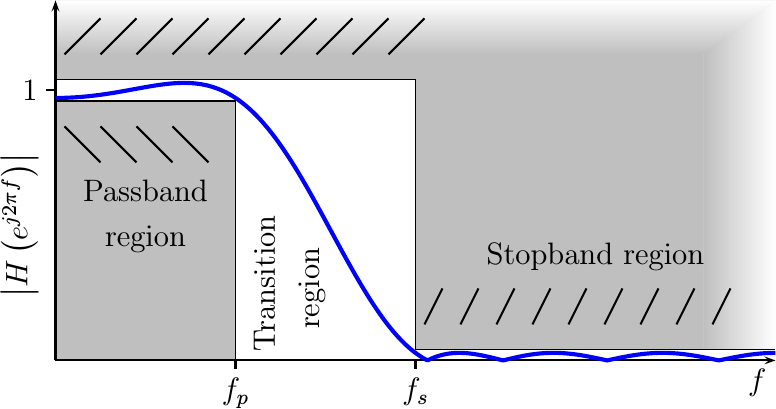
Indeed, this is a good chart for understanding filter design in general. Your goal as a designer will be to create a filter whose frequency response (the blue line) fits within your criteria (the white region). Your application will typically define this white region, although the tighter this region is the more your filter is likely to cost in terms of FPGA resources.
-
Once you know your design criteria, the next step is to determine the number of taps,
N, that your filter will require, as well as an identified number of bits,M, to use to represent the coefficients of these taps. Too many taps or too many bits and your filter will not fit on your FPGA. Too few, and your filter will not match your design criteria above. As a result, filter design is often a give and take between requirements and cost–much like any other engineering task.You may find that the inverse of the normalized transition bandwidth, i.e.
1/(f_s-f_p), is often linearly related to how many coefficients you will need. Two to four times this number, when using normalized frequency units, (i.e.0<f<1/2) is often a good starting place for how many taps your filter will require. As a result of this relationship, any time you drop the transition width by a factor of two, you can expect to need twice as many coefficients for the same cutoff transition bandwidth. -
Design a set of filter filter coefficients using the Parks-McClellan filter design algorithm or similar. Canned filter design methods are usually not hard to find that will generate the filter coefficients you need.
Once designed, then examine the pass band, stop band, and transition band performance to to see how well the resulting filter approximates your design criteria. Adjust as appropriate. More taps for the same criteria can be used to deepen the stopband and tighten up the pass band.
These first steps are common to any Digital FIR filter design problem. The next steps, though, are required in order to try to reduce your bit-width from double-precision floating point to something that can be implemented on an FPGA.
-
Multiply each tap by
(2^(M-1) -1) / max h[n]so that the maximum tap coefficient becomes the maximum positive two’s complement number that can be represented in your bit-width.Since most FIR filters tend to follow the shape of a sinc function, the biggest coefficient will be in the center of the filter. That largest value becomes, by this multiplication algorithm,
2^(M-1)-1. -
Round the rest of the coefficients to the nearest integer.
If we’ve done this right, no coefficients will be greater than
2^(M-1)-1in magnitude.This will also adjust the filter’s frequency response. You may wish to go back and measure your filter’s frequency response at this point to ensure that it’s still within any bounds you application requires.
If this approach seems ad-hoc, that’s because it is. There are more scientific methods to do this. [Ref]
These steps should be sufficient to generate the filter coefficients you will need.
Bit Growth
Once you have the coefficients, the next step is to allocate any bits you need
throughout the design. We discussed
bit growth
some time ago, so we can use those principles for this step.
For the purpose of this discussion, we’ll let IW be the number of bits
in the input samples, TW be the number of bits in the individual coefficients
(we called this M above), and OW be the output width and the width
of the accumulator. These will then be the names we’ll use to define these
values in Verilog parameters later when we actually implement our
filter.
From our
discussion of bit growth,
you know that the multiplication step of the
filter,
the step that calculates h[k]x[n-k], will need to be allocated more bits
to represent the desired outcome than either input. The number of bits
will be the number of bits in the input, IW, plus the number of bits in the
coefficients, TW. Hence, following the multiply you will need TW+IW bits
to hold the output product from one multiply.
Also from the
same discussion,
you know that the number of bits required to add N values of TW+IW bits
together is going to go with the log of N. This means that you will
nominally need TW+IW+log_2(N) bits to hold your result.
This number, though, is often still too many. You can often get by with less
than log_2(N) bits for the accumulation section simply because most of the
taps will be much less than their maximum value, many of them being a factor
of two (or more) less than that maximum
filter
coefficient.
One way to figure out how many additional accumulator bits you will need for
adding the multiplication
results together is to try running a sample signal through the design. The
most stressing case is to let every input have the maximum value,
2^(IW-1)-1, and the sign of the corresponding h[k] tap that it will be
multiplied by. You can then adjust the accumulation width as necessary
to be certain to avoid overflow.
With this as background, we are now ready to consider building our design. We’ll pause first, though, before we get into the Verilog code to discuss our design goals.
RTL Design Goals
For the purpose of the design presented below, we are going to build the most general purpose high speed filter that we can. By “high speed” I mean running at the speed of your system clock—whatever that may be. By “general purpose” I mean three things: First, the number of taps and their values will be arbitrary. They will be fixed at implementation time, but easily adjusted post implementation. Second, I intend to make this filter a reconfigurable filter, so that the values of the various coefficients can be reloaded post-synthesis as the application may require. Third, I intend to create and present a design that can easily (within limits) be adjusted to accommodate more taps, or to adjust tap, data, or output widths, to the design with little change.
Put together, these goals are:
-
Easily reconfigured
-
Adjustable length and variable widths (at design time)
-
Adjustable coefficients (at runtime)
-
Runs at the system clock rate, one input sample per system clock
The sad consequence of these choices is that this is also likely to be one of the more expensive digital filters you will ever build. However, we shall build it anyway and later discuss methods which may be used to reduce this cost. Indeed, such discussions may form the basis of many posts to come.
Chosen Structure
If you look into a text book that describes how an FIR filter should be implemented, you are likely to find a picture looking like Fig 2:
 |
From this figure, you can see conceptually how each incoming data element
goes into a “tapped delay-line” structure (the bar across the top). On ever
clock a new sample comes in, and all the samples within this structure shift
to the right. Also, during that clock, every sample in the delay-line is
multiplied by the respective
filter
coefficient, h[k], and the results
are summed together. The result of this summation is the output of the
filter,
y[n].
The number of “taps”, N, in this figure is easily identified by the number of
stages in the tapped delay line.
What Figure 2 doesn’t show is the second operand, h[k], to each of the
multiplies (they wouldn’t fit in the image). These are given by the
filter’s
impulse response
values–the coefficients that we discussed above.
Were you to try to implement the filter shown in the diagram, you would quickly discover that the accumulator can easily cost many system clock ticks to implement (depending upon the speed of your system clock). Your design may well fail timing as a result. This would be unsatisfactory.
 |
Therefore, we shall consider a different approach. Let’s instead separate the circuitry of one tap from the circuitry of the next, as shown in Fig 3.
The neat thing about this approach is that we can keep the various stages of this filter within a localized area on the FPGA. While that makes timing easier, it still hasn’t fundamentally solved the problem of adding many values together within a single clock. Indeed, the only way to get our clock frequency back up to speed will be to add a clock tick (or more) within this string of taps. The simplest place to do that is between pairs of taps in the accumulator. This leaves us with tap logic shown in Fig 4.
 |
This tap structure
is actually quite unusual. With this approach, the
filter
delay line now requires not N stages but 2N, with the multiplies only
being applied every other stage. Further, it’s not clear from this structure
that all of the additions are being applied to the right values in the
accumulation chain.
For now, I’ll present as a hand-waving evidence that this works the fact that both tap output and accumulator output have been delayed together. When we present the test bench for this design, you’ll see that this is indeed the case. Later, when we convert this filtering structure into something that can handle a symmetric filter, we’ll have to examine how we came up with this approach and explain it in more detail.
For now, notice that by using this tap structure, we can string several of these taps together. An overall view of this strung out design is shown in Fig 5 below.
 |
Indeed, using this approach, we can string any arbitrary number of taps together–subject only to the timing and logic capacity of your FPGA.
The amount of resources this filter will use is likely to become a thorn in our side in a moment, but we’ll ignore that today–for the sake of building the most generic FIR filter.
Before leaving this section, I must acknowledge all of those experts that might also read this blog. Having gotten this far, I am certain that many of these experts are cringing at the design choices we have just made. If you get a chance to chat with them, they will wisely declare that filtering at the full speed of the system clock is resource intensive–it shouldn’t be done if it can be avoided. They will also loudly proclaim that a shift-register accumulator structure is a waste of resources–an accumulator tree might make more sense. Finally, they’ll point out that variable filter coefficients can cost of lot of logic. In deference to these experts, I will first acknowledge the wisdom of their words and then beg their pardon. Today, though, I am trying to keep the filter implementation simple and completely generic.
We can come back to this filter later to improve upon it. All of these improvements just mentioned, and perhaps others as well, are fair game for that later discussion.
In the meantime, let’s examine how to build these two components: the FIR tap structure itself, as well as the tapped delay line structure holding these taps together.
A simple FIR tap
The first component of our
filter
that we shall discuss is the
tap structure.
Remember that our goal is to string
together
many taps with the same code and
structure
to them. Further, you may also remember that the logic necessary for this
tap (Fig 4 above) is primarily multiplying by a filter coefficient, h[k],
and accumulating the result. So, that’s what we’ll do here.
We’ll start with the multiply.
always @(posedge i_clk)
	if (i_reset)
		product <= 0;
	else if (i_ce)
		product <= o_tap * i_sample;
Don’t forget to declare both o_tap and i_sample as signed
values, as the results of a signed digital multiply are different from those
of an unsigned multiply.
On the next clock (multiplies can be slow), we’ll add the result of the
multiply to a partial accumulator value that has been passed to us in
i_partial_acc. This will create our tap’s output, o_acc. After the last
tap, this will be the final output of the
filter.
always @(posedge i_clk)
	if (i_reset)
		o_acc <= 0;
	else if (i_ce)
		o_acc <= i_partial_acc
			+ { {(OW-(TW+IW)){product[(TW+IW-1)]}},
					product };
You may notice in this example that both of these always blocks used a
synchronous reset input. This allows all of the logic to clear, together
with any memory within the
filter,
on any reset. If you don’t need the reset structure, just set the value
to a constant 1'b0 and the synthesizer should remove it. The other thing
to notice is that we are using a global CE based pipelining
strategy.
Under that strategy, nothing is allowed to change unless the CE is true. This
is why all of the subsequent logic is gated by i_ce.
It is worth mentioning that some FPGA architectures can combine the high speed multiply with the accumulation step into one operation. Feel free to design for your hardware as you see fit.
The next required step, though, is to forward the input sample data through a series of registers. At a first glance, this might look simply like,
always @(posedge i_clk)
if (i_reset)
	o_sample <= 0;
else if (i_ce)
	o_sample <= i_sample;
This simple sample in to sample out structure would implement the tap
structure shown in Fig 3 above.
However, were we to keep this logic as is, the outputs from the individual
filter taps.
wouldn’t line up with the accumulator’s output chain. Both would
move through the process at the same speed, and so you’d end up accumulating
H(0)x[n] instead of the desired
convolution.
So, instead, we’ll add an extra delay, delayed_sample, between the
samples–as we discussed with Fig 4 above.
This will allow the partial accumulator structure to remain aligned with the
data as they both work their way through the
tap structures.
always @(posedge i_clk)
if (i_reset)
	begin
		delayed_sample <= 0;
		o_sample <= 0;
	end else if (i_ce)
	begin
		delayed_sample <= i_sample;
		o_sample <= delayed_sample;
	end
That leaves one piece of logic remaining in our
generic tap:
how to set the coefficients in the first place. We’ll choose to do this in
one of two ways, dependent upon the logic parameter FIXED_TAPS.
If FIXED_TAPS is true (not zero), then the parent
module
will feed us our tap
values and we don’t need to do anything with them but use them. While my
preference would be to set each tap via a parameter, this causes a problem
in the parent
module
which would like to set all of the tap values at the
same time via a $readmemh. Instead, we allow our taps coefficients, the
h[k] values we discussed above, to be set from wires passed to this
module. This allows the
parent module
(to be discussed next) to set all of the filter coefficients
via a single $readmemh command within an initial statement.
generate
if (FIXED_TAPS)
	assign	o_tap = i_tap;
else ...
This works well for fixed coefficients, but we still need the logic for our variable coefficient capability.
For variable coefficients, we’ll set FIXED_TAPS to false (i.e. 1'b0).
We’ll also create logic to set our taps dynamically.
Further, each tap will start with an INITIAL_VALUE (typically zero). Then,
during any design run, on any clock where the user is setting taps we’ll just
shift each tap down the line. We’ll use the input i_tap_wr to indicate that
we need to shift the tap value down the line.
This leads us to the following code to set the taps within our design.
...
else begin
	reg	[(TW-1):0]	tap;

	initial	tap = INITIAL_VALUE;
	always @(posedge i_clk)
		if (i_tap_wr)
			tap <= i_tap;
	assign o_tap = tap;
end endgenerate
Notice that here’s no reset in this structure. That allows us to reset the sample values separate from the coefficients. This also allows us to set the coefficients while holding the rest of the filter in reset.
I should warn you: this code can be expensive in terms of logic resources.
Should we count logic resources, you may notice that this requires no LUTs.
The i_tap_wr line can be connected directly to the CE input of the for
tap, and no further logic is required. However, this structure will require
one flip flop per bit per tap in your design. Hence a 256-tap
filter
with 16-bit values will cost you 4096 flip-flops.
The other problem with this dynamic tap coefficient approach is that your synthesis tool cannot optimize any of the multiplies. Logic that might recognize a multiplication by zero cannot be optimized away with this approach. Multiplication by smaller coefficients cannot be trimmed. Neither is it possible to reduce the logic when multiplying by a power of two. Hence, there is a cost for such a dynamic implementation.
As a homework project, try this: Look at how much logic gets used on a per
tap, per bit basis. Then turn on FIXED_TAPS, apply the same coefficients,
and see what changes.
Stringing the taps together into a filter
Now that we’ve defined our tap structures, all that remains is to string them together as in Fig 5 above. This will entail connecting the data inputs from one tap to the next in a streaming fashion, as well as connecting the tap values–should the user wish to change them. Finally, we’ll need to pull our final accumulator value together to return to the rest of the design.
The first step, though, is going to be setting the tap coefficients for
the case where they are fixed. We’d like to do this via a $readmemh
command–since it’s the simplest to do. So, if we have FIXED_TAPS, we’ll
use a $readmemh to set the h[k] inputs to the
filter
tap structures.
On the other hand, if FIXED_TAPS is not true, we’ll only set the first tap
and then let the
tap-modules
push the taps down the line.
We’re also going to use a generate statement, since this will allow us to
use a for loop in a moment.
genvar	k;
generate
if(FIXED_TAPS)
begin
	initial $readmemh("taps.hex", tap);

	assign	tap_wr = 1'b0;
end else begin
	assign	tap_wr = i_tap_wr;
	assign	tap[0] = i_tap;
end
At this point I feel like I’m teaching a drawing class. I’ve outlined two items, and then I’m about to tell the class to just fill in the details. That’s about what happens next.
This next step is to create a for loop where we instantiate each of the taps.
This loop first sets the parameters of
each tap structure
to match our overall
parameters: the input data width, IW, the output width, OW, the width of
the taps, TW, etc. Then we apply the rest of the logic. Each
tap-module is
given an input h[k] coefficient and then connected to an h[k+1] value to
be sent to the next tap.
Each tap-module
is also passed a sample, and it produces the next sample
to be passed down the sample line. Finally, we pass the partial accumulator
from one
tap-module
to the next.
You can see all three of these steps below.
for(k=0; k<NTAPS; k=k+1)>
begin: FILTER

	firtap #(.FIXED_TAPS(FIXED_TAPS),
			.IW(IW), .OW(OW), .TW(TW),
			.INITIAL_VALUE(0))
		tapk(i_clk, i_reset,
			// Tap update circuitry
			tap_wr, tap[NTAPS-1-k], tapout[k],
			// Sample delay line
			i_ce, sample[k], sample[k+1],
			// The output accumulation line
			result[k], result[k+1]);

	if (!FIXED_TAPS)
		assign	tap[NTAPS-1-k] = tapout[k+1];
end endgenerate
When all is said and done, all that remains is to produce our filter output value and we are done.
assign o_result = result[NTAPS];That’s all that it takes to build a generic FIR filter. You don’t need a core generator to do this. You don’t need a GUI. You just need to understand what an FIR filter is, how it operates, and then just a touch of Verilog code. In this case, you can find the code for the tap module here, and the code for the overall generic filter module here.
We’ll save the test bench for another post, as this one is long enough already.
How did we do?
While this is a basic generic digital filter, and while the approach behind it will work for the general filtering case, it isn’t a very powerful filter. The reason is not that this Verilog code cannot describe an arbitrarily long filter, nor is it because this code cannot describe the taps with enough fidelity to create a truly powerful digital filter. Instead, what I mean to say is that this approach to filter implementation tends to be too resource expensive for powerful filters: it is likely to cost too many LUTs, too many multiplies, and in general too much of your precious FPGA’s resources. This may force you to buy a more expensive FPGA, or keep you from having as much free space to do other things on your current FPGA. As a result, we’ll need to do better.
Indeed, we can often build better FIR filters than this.
Here are some basic improvements that we can make to this filter design:
-
We could use an addition tree.
An addition tree would start by adding adjacent values together, then add the results of those adjacent sums and so on rather than adding values together in a long line. This will allow us to use the log base two of the number of additions.
Doing this would remove all the extra data stages, as well as trimming the number of accumulator stages. It would also increase the wire length necessary to send the addition results from one place to the next–but this may be negligible for low enough clock speeds. The problem is that such addition trees aren’t easily reconfigured for different filter lengths–not that they aren’t valuable, useful, or less expensive.
-
We could exploit the structure of the filter coefficients.
Most filter design methods, to include the Parks-McClellan filter design algorithm, produce filters with linear phase. Such linear phase filters have coefficients that are symmetric about some mid-point. As a result, these can be implemented using only half as many multiplies.
-
We could also choose a filter, or combination of filters, that is easier to implement.
For example, a block average is easier to implement than a generic FIR filter. Much easier in fact. A series of block average, one after another, might be able to implement a filter of the type you might need or want. It might also fit nicely as a component of a larger filter.
-
We could fix the filter coefficients
For the design presented above, this is as simple as adjusting the
FIXED_TAPSparameter and creating a hex file containing the coefficients for$readmemh. -
We could use multirate techniques
By “multirate techniques”, I mean that we might include an upsampler or downsampler as part of our filter design and implementation. If we could, for example, downsample the incoming data stream sufficiently, then it might be possible to use a block RAM based tapped-delay line and a single shared multiply for a tremendous resource savings.
These techniques can often form the basis of some of the cheapest filtering approaches, especially when small bandwidths are of interest.
We’ll need to come back and examine these, though we will by no means be able to exhaust this approach to filtering.
The one thing we haven’t done in this post is to generate a test bench for this generic filter. We’ll save that task for a later post–after we’ve created the test bench for our CORDIC algorithm.
Since writing this post, a friend has shown me an even better, cheaper method of creating a generic high-frequency filter. Hence, while the code presented above works, the task could be done without the input sample delay line. We’ll have to come back to that later, therefore, and examine this alternative implementation.
And before him shall be gathered all nations: and he shall separate them one from another, as a shepherd divideth his sheep from the goats (Matt 25:32)