
Driving an output on both edges of the clock
Most FPGA vendor libraries include hardware I/O elements for driving a signal on both edges of a clock. I like to refer to these elements as ODDR modules, since they create a hardware output on both edges, i.e. dual data rate, of a clock. If you are building a design for an FPGA, then I highly recommend that you use such a module.
Sadly, I recently found myself in a position where I couldn’t use a pre-built ODDR on a project. My favorite FPGA vendor I/O libraries weren’t available to me.
Now what?
I needed to build my own hardware DDR output element.
Without a second thought, I scribbled out the following implementation:
module oddr(
	input	wire		i_clk,
	input	wire		i_en,
	input	wire	[1:0]	i_data,
	output	reg		o_pad
	);

	always @(posedge i_clk)
	if (!i_en)
		ddr_data <= {(2){i_data[1]}};
	else
		ddr_data <= i_data;

	always @(*)
	if (i_clk)
		o_pad = ddr_data[1];
	else
		o_pad = ddr_data[0];

endmodule
It wasn’t until some time later that I started wondering if this was really the best way to handle the problem.
Here’s the missing subtlety: we imagine
flip-flop
data changing on a clock tick.
In reality, the clock rises and then only some fractional amount of time later
the actual data changes. During this time between the clock rising and
the ddr_data[1] register changing, there’s the chance such a circuit might
create a glitch,
such as the one shown in Fig. 1 below.
 |
That wasn’t what I wanted.
So I did some internet searching, and came across this lecture on hazards. I quickly learned:
 |
-
That there are three basic types of hazards, each of which might produce a different type of glitch.
-
That with a bit of math, you could not only predict when a hazard might take place, but also lean how to adjust your logic so no hazard would be created.
That left me wondering, could I build something better by just paying attention to a bit of math?
First Draft
My first draft attempted to follow the same logic as my naive approach above. First, I copied the data into a special register.
	initial	ddr_data = 2'b00;
	always @(posedge i_clk)
	if (!i_en)
		ddr_data <= {(2){i_data[1]}};
	else
		ddr_data <= i_data;
Then I needed to find a way to switch between halves of that register.
I thought I might use a cycle variable to capture which half of the clock
cycle I was in. Someone suggested something like the following
	initial	cyclep = 1'b0;
	always @(posedge i_clk)
		cyclep <= !cyclep;

	initial	cyclen = 1'b0;
	always @(negedge i_clk)
		cyclen <= cyclep;
This would require clocking logic on both the positive and negative edges of a given clock. This is in general quite bad, however you are kind of stuck with doing something on both edges of the clock to build a circuit like this in the first place. At least I was only looking at one register.
The last step would then select between which of two bits based upon
whether these two cycle* registers matched.
	always @(*)
	if (cyclep ^ cyclen)
		o_pad = ddr_data[1];
	else
		o_pad = ddr_data[0];
But was this better?
At this point, I tried applying the math from the slides I had
found. This required
expressing my design as either a sum of products, or a product of sums. So,
I rewrote the logic for o_pad as a sum (OR) of products (ANDs).
	always @(*)
	begin
		o_pad =    (ddr_data[1] &&  cyclep && !cyclen)
			|| (ddr_data[1] && !cyclep &&  cyclen)
			|| (ddr_data[0] &&  cyclep &&  cyclen)
			|| (ddr_data[0] && !cyclep && !cyclen);
	end
Now, if you suppose that ddr_data[1] == ddr_data[0], and look for
glitches,
you’ll find a couple of static zero
glitches.
The same slides suggested that I should add a fifth term to avoid these hazards.
	always @(*)
	begin
		o_pad =    (ddr_data[1] &&  cyclep && !cyclen)
			|| (ddr_data[1] && !cyclep &&  cyclen)
			|| (ddr_data[0] &&  cyclep &&  cyclen)
			|| (ddr_data[0] && !cyclep && !cyclen)
			|| (ddr_data[0] && ddr_data[1]);
	end
By the time I got this far, I was feeling pretty proud of myself: I had just discovered that my system would glitch. Not only that, I’d also figured out how to keep it from glitching.
I was so proud of myself, that I wanted to see how this circuit would look. So, I ran Yosys to get a peek at it.
% yosys -p 'read -sv oddr.v; synth -top oddr; show'The result was Fig. 3 below.
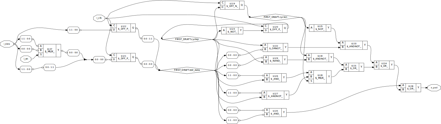 |
If I stared hard enough at the figure, I could see all of my logic carefully laid out within it.
Nice.
But then I got to wondering, what would the logic optimizer do to a circuit like this?
So, I ran a pass of ABC followed by the Yosys optimizer.
% yosys -p 'read -sv oddr.v; synth -top oddr; abc; opt; show' |
The result was that all my special glitch-reducing logic had been removed. It was redundant. Sure, the optimizer did what I would expect, but how should I now fix my circuit?
Worse, as I looked over my draft further, I could quickly see that this combinatorial equation was much more complicated than I would ever want to have driving the output of a chip. There was just too much room for error.
I needed something simpler.
A Better Approach
Here was the rub: no matter how I built the circuit, I was going to need some combinatorial logic past the last clock. Further, if I wanted to avoid using the clock itself in my output, then I was going to need to transition on both edges of the clock. There was no way around that.
This left me with the following structure.
- First, I would need to do something to my inputs, to transform them somehow into local registers to this module. This would happen on the positive edge of the clock–and would work like any other piece of logic I might use in my design.
	always @(posedge i_clk)
positive_edge_logic = f0(inputs);- I would then need to move one of those pieces of logic from the positive to the negative edge of the clock.
	always @(negedge i_clk)
		negative_edge_logic = f1(positive_edge_logic);
Although I’ve shown this as a predicate logic function, f1, in reality this
needs to be just a register copy since time is important and I want to make
certain that nothing gets lost in this translation–especially since I’m
not sure how well I trust my tools to handle this logic.
- The third step would then be some form of logic function on the two halves: the logic generated on the positive edge of the clock and the logic created on the negative edge.
	always @(*)
o_pad = f2(positive_edge_logic, negative_edge_logic); |
I also wanted to keep this third function simple. Something that would not only
be glitch free,
but would also be simple enough to not have a lot of logic
delays within it. While both AND and OR might work individually, they
would both require the inputs change on both edges of the clock–there would
be no way to “undo” the output from one clock half once the next clock half
arrived. In the end, I decided that f2 above needed to be an
exclusive OR (XOR)
function–especially since an
XOR can be accomplished
simply with a small number of transitors. Not only that, it’s a basic
standard cell element in most
ASIC logic libraries.
That left me with something like Fig. 5 above and on the left and written out below,
	always @(posedge i_clk)
		{ cp, cnp } = f0(inputs);

	always @(negedge i_clk)
		cn <= cnp;

	always @(*)
		o_pad = cp ^ cn;
cp and cn would be the outputs of
flip-flops
set on positive and negative edges of the clock respectively. cnp, on the
other hand, would be an intermediate result used to pre-calculate the logic
for the negative
flip-flop.
But what should I use for the positive clock edge logic?
For that, I worked both clock phases out independently.
For the first phase of the clock, I’d be able to control the cp of the
cp ^ cn function. In order to output the first data element on the
positive edge of the clock, I only needed to annihilate the cn.
	always @(posedge i_clk)
		cp  <= i_data[1] ^ cn;
Unfortunately, this made for a second and unnecessary clock domain crossing,
from the negative edge of the clock to the positive edge. On the other hand,
cn was just a copy of cnp from the prior positive edge of the clock,
so I could just as easily reference cnp instead without incurring any
additional edge-to-edge crossings.
	always @(posedge i_clk)
		cp  <= i_data[1] ^ cnp;
Generating an equation to set cnp would’ve been just as easy, except I needed
the new value of cnp to depend upon the result of cp which was still being
calculated on this same clock period. If I just place a parenthesis around the
new cp value, then the equation becomes almost identical as the one for cp
above.
	always @(posedge i_clk)
		cp  <= i_data[0] ^ (i_data[1] ^ cnp);
But would it work?
To double check my work, I fired up SymbiYosys.
No, SymbiYosys can’t handle analog logic–which is really what this attempt at glitch-free logic is. However, it can handle digital logic on both halves of a clock. That was what I wanted here for a quick check.
Formal methods check
Thankfully, the formal check of this
logic is fairly easy. The first step is
to use the multiclock on option within the
SymbiYosys
configuration file.
Once done, you’ll need to assume the existence of a toggling
clock–taking
two formal timesteps per clock cycle.
`ifdef	FORMAL
	(* gclk *) reg	gbl_clk;
	reg	[1:0]	f_data;

	always @(posedge gbl_clk)
		assume(i_clk != $past(i_clk));
I then needed to assume the inputs were clock synchronous.
	always @(posedge gbl_clk)
	if (!$rose(i_clk))
		assume($stable({ i_en, i_data }));
Or, rather, I forgot to include this assumption at first and then got surprised when the result wasn’t what I wanted. When the design then failed, resulting in a trace where the inputs didn’t “look” right, I figured I should add the assumption above.
The last step to setting up the problem was to keep track of the bits I wanted
to output. I used a quick two-bit register, f_data, for this purpose.
	initial	f_data = 2'b00;
	always @(posedge i_clk)
		f_data <= i_data;
The last step was the assertion: I wanted to make certain that the result was correct on each half of the clock.
	always @(*)
	if (i_clk)
		assert(o_pad == f_data[1]);
	else
		assert(o_pad == f_data[0]);
Yes, this looks just like the logic I started with that I am trying to replace.
Indeed, it did do–although I did initially need to skip the first couple of time-steps until everything sync’d up. Still, it worked quite nicely to help me figure out what I was doing right and wrong.
Polishing off the design
The last step was to implement the “off” function, where the ODDR module wasn’t enabled. My first thought was that I should keep the output from toggling when not enabled. A second thought was that I should just set the pins to the first bit of input.
Adjusting f_data was the easiest way to at least describe what I wanted.
	always @(posedge i_clk)
	if (!i_en)
		f_data <= {(2){i_data[1]}};
	else
		f_data <= i_data;
From here, I could design something that met my formal criteria and SymbiYosys could then tell me if I got it right or not.
My first draft for this logic was just to set everything to a constant if ever the enable input was low.
	always @(posedge i_clk)
	if (!i_en)
		{ cp, cnp } <= (i_data[1]) ? 2'b01 : 2'b00;
	else // ...
Only … this didn’t pass the formal check.
After a little bit of floundering, I realized I would have to build this based
upon cnp. That led me instead to the following logic.
	always @(posedge i_clk)
	if (!i_en)
	begin
		if (i_data[1])
			{ cp, cnp } <= (cnp) ? 2'b01 : 2'b10;
		else
			{ cp, cnp } <= (cnp) ? 2'b11 : 2'b00;
	end else begin
		cp  <= i_data[1] ^ cnp;
		cnp <= i_data[0] ^ i_data[1] ^ cnp;
	end
Even better, the result is pretty simple logically. It only requires three XOR elements, three flip-flops, and a mux. Even better, as designed above, the output is driven by an XOR of two flip-flop outputs.
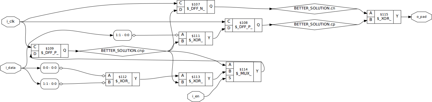 |
Not only that, this circuit will not glitch–assuming the XOR can be implemented as a single gate.
Conclusion
This entire exercise was a lot of fun, and I learned a lot about glitchless logic in the process.
How practical is this design? Well, it’s not portable to any FPGAs. Indeed, I wouldn’t use it on an FPGA at all. There are better structures on FPGAs, and those structures are ideally placed on the FPGA to handle final timing properly.
See, that’s the big problem with this design: it’s highly susceptible to placement. Were the XOR placed on the opposite side of the chip from the pad it is driving, you might easily have multiple pins transitioning on apparently separate clocks. Even if the XOR were placed next to the pad, flip-flop placement will adjust both clock period and phase. That means that in order to make this work properly, you’ll need to make certain that both the flip-flops and the XOR are placed right next to the output pad. That places further requirements on the tools you use and what they need to support in order to make this happen.
So, is this doable? Absolutely! Is the task done? Far from it. Still, it was a fun distraction for a evening.
Are not two sparrows sold for a farthing? and one of them shall not fall on the ground without your Father. (Matthew 10:29)