
How to build a SPI Flash Controller for an FPGA
 |
Perhaps you may remember that I’ve been working to port the ZipCPU to an iCE40 HX8k platform: the ICO board. I like to boast that the ZipCPU was designed for low logic applications, and the iCE40 is certainly a low logic chip. While the ZipCPU isn’t the smallest processor out there, there are some forth processors that are much smaller, it does fit nicely with room to spare on the iCE40 8k.
However, if you want a design that starts immediately upon power up, or if you want more memory than is available in 8kB of block RAM or (in this case) even in 128kB of SRAM, then you need access to the flash memory. Why? First, flash memory is non-volatile, so anything that reads from it can do so immediately upon power up. Second, most FPGA’s need a flash chip to store their design within, so flash chips are a common addition on FPGA boards. Third, flash is fairly cheap: a single 16MB flash chip can sell for as little as $1 on Digikey. Given that my ZipCPU design logic for the ICO board only requires about 132kB of memory, that leaves me with lots of memory to play with … if I just had a simple flash controller.
I also had another reason for this project as well: I wanted to learn about System Verilog sequences, and whether or not they could be used to formally verify a flash controller. Yes, I had access to the full commercial (Verific enabled) version of yosys to do this. But I wanted to see how useful this full version would be when it came to designing a new/better flash controller.
So let’s see what it takes.
Lessons learned from other flash controllers
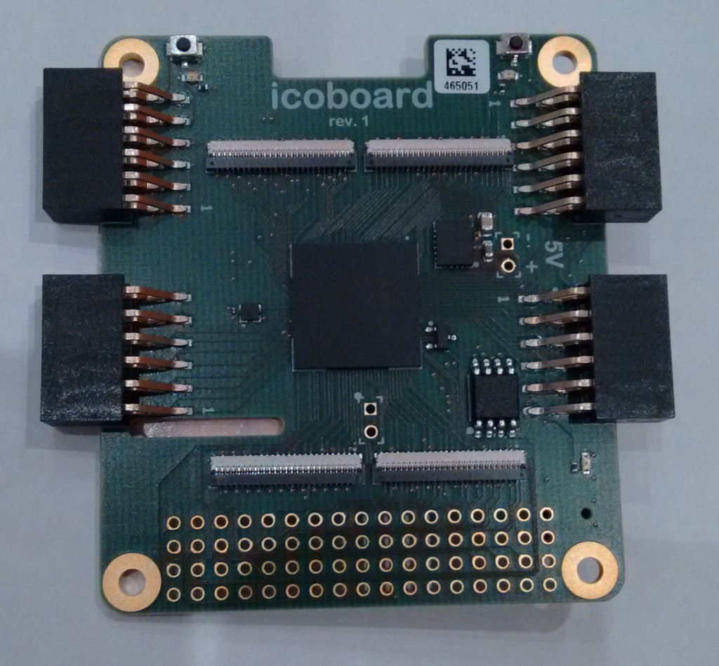
When I start any new design, my first step is to download the schematic for the board that I have, and data sheets for all of the parts. In this case, the ICO board has a Cypress S25FL127S 128 Mbit (16MByte) chip connected to the iCE40 FPGA. I then spend some time reading the specifications and studying the schematic before building anything.
In this case, by the time I came to this board’s flash, I had already built several flash controllers before.
 |
-
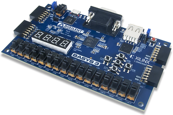
The first flash controller I ever built was for the Basys-3 board. This board had a Spansion S25FL032P 4MB flash. Since it was my first flash controller design, my goal was to design something that could do everything:
– It could read the flash at both high (QSPI) and low (SPI) speeds
– It could read the flash’s internal configuration register in order to determine if the QSPI mode was even enabled
– It could both erase and program the flash
– It could be used for reading the vendor identification words back from the flash, and
– It could be used for reading the status register and/or writing the configuration register of the flash.
This was a great general purpose flash controller, and I’ve used it many times since. However, all of this extra logic has consequences when you want to place your design on a small board. How bad? It consumed about 1263 of the 7680 cells on an iCE40, or about 16% of the entire FPGA logic.
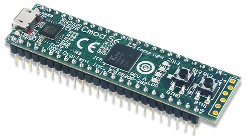
The other problem I had with this design was when I tried to place it onto the Spartan 6/LX4 of the CMod S6. Sure, there was plenty of room for the controller and the debugging bus I was using at the time–there just wasn’t much room for anything else.
 |
-
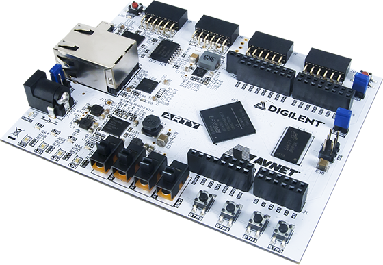
Sometime later I decided I wanted to build a high speed flash controller, so that I could push Digilent’s Arty up to a system clock rate of 200MHz. Why 200MHz? Because I had mistakenly thought this was the clock speed I’d need to use to interact with the DDR3 SDRAM on board. When I realized I couldn’t interact with the SDRAM any faster than about 82MHz, I abandoned this controller and never used for any other projects.
Still, if the last controller was full featured, this one was even more so. It not only allowed you to read and write any of several configuration registers, it would also allow you to read and write the one-time programmable (OTP) ROM. Further, since I wanted this to run at 200MHz, there was a lot of pipelining (and extra latency) to this controller.
In hind sight, this controller was a boat anchor. It’s bloated with features I never used and as a result was way too big for the job.
 |
-
However, when I needed to upgrade the ZipCPU in my S6SoC design so that it would support 8-bit bytes (the ZipCPU was originally a 32-bit byte architecture), I needed to find spare LUTs anywhere I could. 2,400 6-LUTs isn’t a lot of room for a multi-processing CPU, and so I had to strip everything out that I could.
The first thing to go was everything but the read capability from the flash controller. That removed 30% of the logic in the controller.
It wasn’t enough.
Then I stepped back and realized that I would only ever run the ZipCPU from an already programmed flash, and that all I ever really needed from the flash was the ability to read from it. I didn’t need to be able to read the status register, the configuation register, the vendor’s ID, or anything else: I just needed to read the flash memory.
I also needed speed.
So I created a flash memory controller that used the Spartan 6’s DDR capability so that it could read from the flash at the system clock speed. This provided a rough 2x improvement in speed. Further, the rewrite to create this capability, and this capability alone dropped the number of LUTs used by the flash from (roughly) 569 down to about 100 or so.
(These numbers are approximate because yosys doesn’t yet pack Xilinx LUT’s together, but they do give an idea of usage.)
Since this controller offered only a read capability and nothing more, I called it my
qflashxpresscontroller.
 |
-
I recently started working on a fourth flash controller modeled after this last one, but using the Dual SPI read mode of the flash. This controller is designed to support the iCE40 on the TinyFPGA BX. However, on my pre-production version of the TinyFPGA BX, only the MISO and MOSI lines are connected to the flash, so the best/fastest I could ever do is Dual SPI which would only allow me to read/write two bits at a time. (I have been assured that this has been fixed for the production versions.)
Unlike the previous qflashxpress controller, I wanted the erase/program capability back. Rather then teach the HDL controller all of the necessary states associated with erasing and reprogramming a flash, I initially created a bit banging port that could override the natural logic of the port.
The more I thought this through, though, the more I realized that bit banging over the debugging bus would be horrendously inefficient. Better yet, the code already had the capability to send data to and receive data from the flash, why not just adjust the configuration access so that it can command an 8-bit transfer?
That leads me to the basic flash controller I want to discuss today.
Why do I need a new flash controller? For a couple of reasons. The first and perhaps more important is the reality of how the ICO board was wired.
 |
In order to make certain that both the Raspberry Pi and the iCE40 could control the flash memory, the memory was routed through a MachXO2 chip as a traffic controller. However, the MachXO2 as wired has no capability of dynamically controlling pin direction–the pins can only ever go one way–either master in and slave out (MISO), or master out and slave in (MOSI). In other words, any flash controller for the ICO board can only ever use the traditional SPI mode, and thus any DSPI or QSPI enabled controller will only consume excess and unused logic in an already tight space.
All this is to say that this is my now a fifth generation flash controller for me. I’ve also learned along the way what’s important in a flash controller:
-
First and foremost, the controller: must be able to read from the flash. It must do this function well and fast, since this is its purpose for being. As you’ll see, with no other logic this will cost us 147 of the 7680 cells on the iCE40.
If I wanted, I could stop here. Nothing more is really required.
-
Second, as an optional performance improvement, it should be able to read data from the flash in long strings of uninterrupted transactions. Adding this logic to the controller will eventually cost us another 88 iCE40 logic cells.
-
Third, as a second optional enhancement, it needs to support a single configuration register providing access to the rest of the flash’s capabilities without burdening the flash controller with unnecessary features. This final feature will cost an additional 38 logic cells, bringing our entire total up to 273 logic cells out of 7680, or about 3% of the entire design.
This is a reasonable usage number for our purposes.
That’s the controller we’ll examine today.
Basic SPI
If you are not familiar with the Serial Peripheral Interconnect (SPI) means of communicating between digital components, then let me recommend the SPI article on fpga4fun.com. It’s short, and it explains a lot of good details about the SPI protocol that you might find valuable. In sum, it describes what can be a shared bus, with typically a single master and many slaves, operating over a synchronous (i.e. clocked) interface.
 |
The basic wires associated with this interface are:
-
CS_n, a ‘negative logic’ chip select sometimes calledSSfor the “slave select” line. This is the one line that is unique to each bus slave. It is used to create a capability whereby multiple chips can have access to the SPI bus at the same time. The “master” simply selects the one chip it is interested in. The other chips are then required to place their output pin into a high impedance state and to ignore any transactions for which they are not selected.This means that anytime
CS_nis high, the chip of interest is not selected and all of other wires are “don’t cares”.The
CS_nsignal is also be used for synchronization. Pulling this wire low (active) signals to the slave the beginning of a transaction, and hence the slave knows which bit is the “first” bit of the transaction packet.Today, we’ll be focusing on the interaction associated with a single chip.
-
SCKis the serial clock. Since this is a clocked interface,SCKprovides that clock. The SPI protocol allows for several definitions of how this clock needs to be implemented, so check the chip you wish to interface with to double check for example the polarity and phase of the clock signal that it is expecting.For our implementation below, we’ll insist that
SCKbe high any timeCS_nis inactive, even though technically this is a “don’t care” signal in such cases. -
MOSI. I pronounce this wire as “MOH-see”, although it’s technically the acronymn, “Master Out Slave In”. Some chips will call this wire SDI for Slave Data In or even just SI for Slave Input. This is the one wire running from the master to all of the slaves containing information coming from the master.As with the clock, pay attention to your chips specification of this signal. We’ll treat this signal today as a signal that can only change on the negative edge of
SCK. -
MISO, or “MEE-soh” as I like to pronounce it, is the “Master In, Slave Out” wire–a single wire interface shared among all SPI slaves and containing the data being returned from the selected slave device. Some chips will call this wire SDO for Slave Data Out, or even SO for Slave Output. All of these terms refer to the same basic wire.Check the specification of the chip you are working with for details on this signal, but from my experience this signal tends to change some number of
nsfollowing the last negativeSCKedge. It should be stable wheneverSCKis high, as long as you don’t makeSCKrun too fast, so you can read it any timeSCKis high.
These are the basic signals we’ll be working with.
A SPI
flash doesn’t typically use the
full interface capabilities, however. Instead, every
flash
SPI
protocol I’ve read about has actually been a
Simplex,
or one-way, protocol. The basic
flash
transaction involves sending an 8-bit command, followed by any command specific
arguments (if any–depends upon the command), after which the slave will
return some kind of response. In no part of this process are both MISO and
MOSI lines containing valid data going in opposite directions at the same
time.
Either the
flash
controller
is sending data to the flash chip,
or the data is going in the reverse direction.
 |
If you examine the specification for the Cypress Flash device on the ICO board, and look closely through it, you’ll quickly discover that all transactions are composed of sequences of octets (8-bits)–just like we discussed above. This is common among SPI based flash chips.
Those first 8-bits of the transaction, though, are the important ones. Hence the spec outlines all the different commands that can be started from any 8-bit value. The command set is rather long, though, stretching across both page 109 and 110–so I’ll only reference it here. Further, there’s a whole chapter devoted to walking through each of the commands in detail.
 |
This simplex
command response protocol also allows particular bastardizations of the
SPI
protocol whereby the MISO and MOSI lines are re-purposed into bi-directional
wires: the master might send on both bits during the argument period of the
command, and then receive on both bits during the response period. This is
called “Dual SPI” mode, or DSPI for short. Many
flash
chips (including this one)
also have two other wires, a negative logic reset/hold pin and a negative logic
write protect pin. These can also be re-purposed into further bidirectional
data wires, creating a four-wire bidirectional data bus for even faster
communication. This four wire mode is often called “Quad SPI”, or QSPI
for short.
Today, we’ll be looking at two basic capabilities, both within the basic
SPI protocol.
The first capability will send a read command to the
flash,
and then read data back in the response. This will be our basic read
capability. The second will send an arbitrary 8-bit command to the flash,
and then maintain the CS_n pin low and the SCK pin stable (and high) until
either another command is received, or our
controller
is explicitly told to adjust them again.
Read only
If you look through the command table on page 109 of the specification for
this chip, you’ll notice several
commands that can be used to read from the
flash. There’s the READ
command which tops out at a maximum SCK clock rate of 50MHz, the
FAST_READ, topping out at 108MHz, the DOR or dual read output, and the
QOR or quad read output. There are also some faster read commands, such as
the DIOR or dual I/O read and the QIOR or quad I/O read. There are also
4-byte address commands, although they are not required on this flash.
From my own experience, I have found that the reads delivering 4-bits at a time are the fastest, especially when you can start the transaction immediately with the address in what is sometimes called XIP mode–but we’ll have to leave that discussion for another day, since the ICO board layout doesn’t support these high speed access modes.
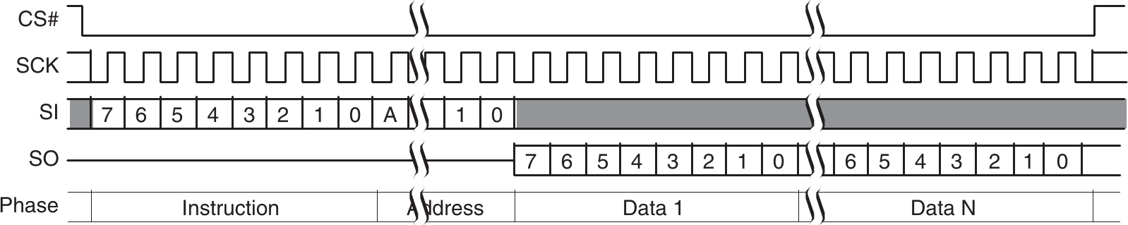
So let’s return to the basic READ command. This command starts from
the device in its idle or default state, requires the controller to send an
8-bit READ command to the device (8'h03), followed by a 3-byte (24-bit)
address. Once done, the device will return bytes to us in sequence from the
flash, starting at the
address we give it and incrementing by one for each byte read.
The spec shows a picture of this operation for us, which I’ve copied below into Fig 10.
 |
Unlike many of the other things we’ve discussed, a flash interaction is very much an organized interaction over many clock cycles. Let’s copy our interaction into wavedrom where we can edit it, and then take another look again.
 |
This now becomes our goal–the specification our component must match.
One key point in this picture is the clock rate. The device will limit our
maximum SCK rate to 50MHz when using the basic read command, 8'h03. Given that my goal system clock rate for this
design is 50MHz as well, this will work well.
But how to get an SCK of 50MHz from a 50MHz system clock? To do this, we’ll
use
a DDR output function of the SB_IO primitive provided by the
iCE40.
That will allow us to run all of our logic at full speed,
even though this clock signal will toggle twice as fast as our logic.
Before moving forward, let’s add one more design requirement to the
waveform file in Fig 11: Our
flash
controller
must also interact with a Wishbone
bus. Let’s think about
how we’ll do this for a moment. Ideally, the
controller
will need to accept a request from the bus, and then immediately
start the read transaction with the
flash chip. Once done, the
controller
will need to return a response, o_wb_ack and
o_wb_data, to the same bus. All in all, this should look something like
Fig 12 below. In between the request and the acknowledgment, the o_wb_stall
signal should be high.
 |
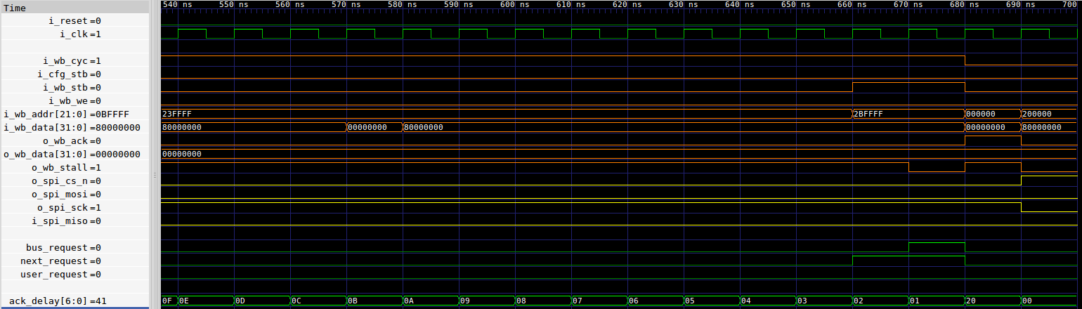
Notice also that I added two other control wires to this picture: ack_delay
is an internal counter, and o_spi_sck is an output from our
controller
to the DDR output
module.
The ack_delay counter will be used to keep track of where
we are in the sequence. This is shown at the bottom of Fig 12 above. Once
ack_delay hits zero, we should be done with our transaction. If you look
in the sequence above, you’ll notice that the same clock ack_delay hits
zero is also the clock o_wb_ack is high, o_wb_data is valid, o_wb_stall
returns to zero, and CS_n returns high.
The o_spi_sck signal also needs a bit more explanation. This isn’t the
actual SCK signal going to the
flash chip, but rather
a signal to the DDR output
module
telling it to toggle the clock. You may notice that this signal is set
immediately after the
Wishbone
strobe (request) signal is accepted (i.e. strobe is high and stall is low).
However, the SCK signal doesn’t start toggling for another clock period
after setting this o_spi_sck signal high. (This was unexpected, and so
we’ll discuss this again in our testing section below. This one clock change
forced me to delay all of the other signals by one clock, as already shown in
Fig 12 above.
For now, though, let’s return to that ack_delay signal and just point out that
we’ll be using this signal internally to control a basic state machine.
We’ll start our state machine with a “bus request”: a request to read from the flash memory. That will look something like:
wire	bus_request;
assign	bus_request = (i_wb_stb)&&(!o_wb_stall)&&(!i_wb_we);
We can then use this bus_request signal to start our ack_delay counter.
Once started, ack_delay will just count down to zero, when we will
acknowledge the bus request.
initial	ack_delay = 0;
always @(posedge i_clk)
if (bus_request)
	ack_delay <= 6'd65;
else if (ack_delay > 0)
	ack_delay <= ack_delay - 1'b0;
The second piece of circuitry we’ll want is a shift register controlling the
MOSI values that we send to the
SPI
interface. This will include both our command, 8'h03, and the address we
wish to read from, { i_wb_address, 2'b0 }. (The last two bits are zero,
because the Wishbone
address is a word address, not a byte address.) Since we know the address at
time zero when the bus_request is made, this can be as simple as,
always @(posedge i_clk)
if (bus_request)
	// Here's the data stream we wish to send
	wdata_pipe   <= { 1'b0, 8'h03, i_wb_address };
else
	wdata_pipe <= { wdata_pipe[31:0], 1'b0 };

assign	o_spi_mosi = wdata_pipe[32];
Note the extra zero bit out front. This is due to the extra clock it takes to
start the DDR SPI
SCK signal that we mentioned above, and diagrammed in Fig 12.
All that remains is to set the rest of our signals based upon this counter,
using Fig. 12 above as a guide. Remember, signals that are set on the
positive edge of a clock need to be set one clock before they are to be valid.
Hence, if you want to set the CS_n signal high so that it is
high when ack_delay returns to zero, you’ll want to set it that way when
ack_delay is 7'd1.
First, upon a bus request, we would get things started.
always @(posedge i_clk)
if (bus_request)
begin
	o_spi_cs_n <= 1'b0;
	o_spi_sck  <= 1'b1;

	o_wb_ack   <= 1'b0;
	o_wb_stall <= 1'b1;
Then, while things are running, we update any signals.
end else if (ack_delay > 1)
begin
	o_spi_cs_n <= 1'b0;
	o_spi_sck  <= (ack_delay > 2);

	o_wb_ack   <= 1'b0;
	o_wb_stall <= 1'b1;
	o_wb_data  <= { o_wb_data[30:0], i_spi_miso };
Once we get to the end, we’ll need to shut down our interface and return an acknowledgment and our data. We can also turn the stall signal off at this time.
end else if (ack_delay == 1)
begin
	// Turn off the interface
	o_spi_cs_n <= 1'b1;
	o_spi_sck  <= 1'b0;

	o_wb_ack   <= 1'b1;
	o_wb_stall <= 1'b0;
	o_wb_data  <= { o_wb_data[30:0], i_spi_miso };
Finally, if ack_delay==0 and there’s no bus_request, then we just want
our interface to remain idle. We’ll also quietly ignore any write requests
from the bus, acknowledging them immediately while we are idle.
end else begin
	// Interface is idle
	o_spi_cs_n <= 1'b1;
	o_spi_sck  <= 1'b0;

	o_wb_ack   <= (i_wb_stb)&&(i_wb_we);
	o_wb_stall <= 1'b0;
end
This is our primary capability. We could ideally stop here if all you wanted was a simple flash controller to only read from your flash.
Second: Piped reads as well
One problem with stopping here, though, is that this approach to reading from a flash memory is painfully slow–especially for a soft-core CPU when its speed is limited by the speed it can read instructions from the flash. If you just count clock cycles, then the controller as is takes 66 cycles per read. This will limit any CPU’s speed to 66 cycles per instruction (CPI). While this may be faster than your average snail, I’d like my CPU to run a bit faster.
If you remember our discussion about pipelining a prefetch, then you’ll remember how I managed to keep a rolling prefetch going in the presence of a flash device. That would increase the speed of a flash bound CPU from 66 CPI (minimum) up to 33 CPI. It’s still a snail’s pace, but a factor of two better is still a factor of two.
How might we do this?
The first step is to go back to the specfication for our flash chip, and then to remember that once the read is started the flash will just keep producing subsequent bytes. This is what we’d like to capitalize on. We could do this if we just kept the transaction going for another 32-bit word, but only if there was a request for the next word from the bus. We’ll have to test for that in a moment.
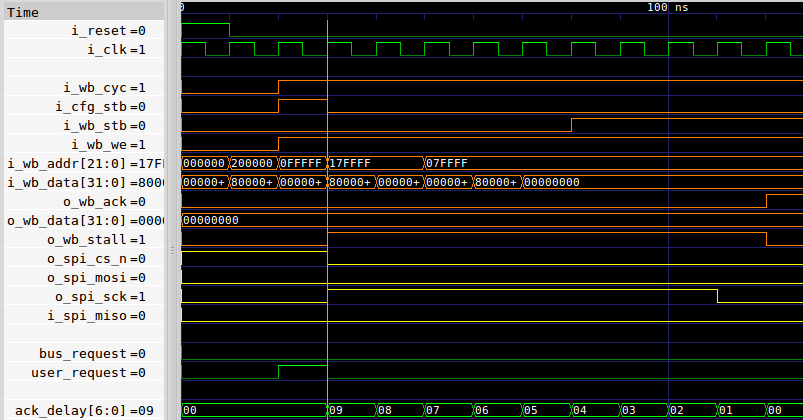
We’ll start this modified design by returning to our timing diagram. Specifically, we’d like to be able to accept a request for the next address just in time so that we don’t lose any clock cycles in our SPI transaction. Hence, if we were just about at the end of one transaction, then we should be able to extend it by one more transaction, as shown in Fig. 13 below.
 |
Notice a couple key points here. First, the ack_delay line never hits
zero–it just immediately goes into the next word. The o_wb_ack and
o_wb_data lines maintain their requirement, they are to be valid one
clock after ack_delay==1. Indeed, in many
ways, this looks identical to what we had before with the exception that
following a bus_request for the next word we go immediately into reading it
instead of sending a new address.
Our first problem in this picture is the stall line–it needs to be low one
clock early, or when ack_delay==1, and not when ack_delay returns to zero.
The only thing is, we can’t do this at all times, but only when
the address requested is for the next word, only when this is a read request.
That’s going to require some extra logic.
It also requires a little bit of trickery that doesn’t quite follow the
Wishbone
specification:
we’ll take a peek at any pending transaction on one clock and set a flag
based upon it,
then we’ll check that flag and drop o_wb_stall if necessary on the
following clock. This new flag, next_request is shown at the bottom of
Fig. 13 above.
So here’s the extra logic. First, we’ll capture the next address.
	reg	[21:0]	next_addr;

	always @(posedge i_clk)
	if ((i_wb_stb)&&(!o_wb_stall))
		next_addr <= i_wb_addr + 1'b1;
Then, we’ll put our next_request flag together.
assign next_request = (i_wb_stb)&&(!i_wb_we)&&(i_wb_addr == next_addr);Now we can come back and review our basic signals from before.
The MOSI signal is a don’t care, so we can keep our wdata_pipe logic
simple.
The logic for CS_n doesn’t change either–it’s set to zero on any bus
request, and this pipe request (once the stall is lowered) is just another
bus request.
The ack_delay logic does need to be adjusted, but this is minor. Specifically, if there’s a bus_request where CS_n is already low, then only set
ack_delay to 32 instead of 65.
	initial	ack_delay = 0;
	always @(posedge i_clk)
	if (bus_request)
		ack_delay <= (o_spi_cs_n) ? 7'd65 : 7'd32;
	else if (ack_delay != 0)
		ack_delay <= ack_delay - 1'b1;
The SCK and o_wb_stall signals are a touch more difficult. First, the
SCK signal needs to remain high one clock longer if next_request is high.
	initial	o_spi_sck = 1'b0;
	always @(posedge i_clk)
	if (i_reset)
		o_spi_sck <= 1'b0;
	else if (bus_request)
		o_spi_sck <= 1'b1;
	else if (ack_delay > 2)
		o_spi_sck <= 1'b1;
	//
	// NEW LOGIC: keep the clock going if there's a second request
	// coming.
	else if ((next_request)&&(ack_delay == 2))
		o_spi_sck <= 1'b1;
	else
		o_spi_sck <= 1'b0;
Second, and really this is the key piece of logic on which all the others
depend, the stall line needs to be lowered
so the request can be accepted in time to start the new transaction without
any delayed cycles. This pins the stall low clock period to be the same
clock period where ack_delay is one.
	initial	o_wb_stall = 1'b0;
	always @(posedge i_clk)
	if (bus_request)
		o_wb_stall <= 1'b1;
	//
	// NEW LOGIC: Drop the stall line if a request for the
	// next address is pending.  The stall line will be
	// low in this case when ack_delay == 1.
	//
	else if ((next_request)&&(ack_delay == 2))
		o_wb_stall <= 1'b0;
	else
		o_wb_stall <= (ack_delay > 1);
Notice how these changes are fairly minor, but yet they can speed up a CPU’s instruction fetch by a factor of two (… but only if the CPU doesn’t use the bus for data, doesn’t branch, doesn’t … etc). There are some CPU speed details in there that I’m glossing over. Still, we haven’t changed our logic all that much to get this additional capability.
At this point, we could stop again. We’d now have a faster ROM
flash device. The
flash would need to be written
using some other configuration, but we’d be able to read it in high speed.
But, couldn’t we get the ability to read and write the flash for just a little bit more work? That’s the purpose of the configuration port that we’ll discuss next.
Third: Configuration port
Can we add a configuration port capability to this flash controller? Specifically, it would be nice to have access to all of those other commands outlined in the flash specfication.
Let’s use a separate
Wishbone
port for this purpose. By that I mean, let’s create a separate strobe signal,
i_cfg_stb,
but otherwise share all of the signals between these two ports. The bus
interconnect
can then set this new strobe signal, i_cfg_stb, to indicate
a request on this new port.
Unlike the primary Wishbone
bus,
we’ll make this one so that you can both write and then read
from this port. Write’s will send 8-bits to the device over the MOSI line,
and reads will read the 8-bits returned in the MISO line. In order to
allow longer interactions, extending beyond a single 8-bit transaction,
we’ll allocate bit i_wb_data[8] and use it to control the CS_n bit.
Fig. 14 below shows this concept of this protocol.
 |
Writes with i_wb_data[8] low will cause 8-bits to be sent, reads will
return the response. Writes with i_wb_data[8] set will return the
device to the mode where we can read data again.
Were we building only this interface, the logic would look very similar to
just the logic necessary to implement Fig. 14 above. We’d start with an
user_request signal, capturing the write request on this configuration
channel.
	wire	user_request = (i_cfg_stb)&&(!o_wb_stall)&&(i_wb_we)
				&&(!i_wb_ata[8]);
Then we could just walk through our basic signals again.
We’d start with the MOSI signal. This was based upon a wdata_pipe
shift register before. We can do this again now.
	initial	wdata_pipe = 0;
	always @(posedge i_clk)
	if (user_request)
		wdata_pipe <= { 1'b0, i_wb_data[7:0], 24'h0 };
	else
		wdata_pipe <= { wdata_pipe[31:0], 1'b0 };

	assign	o_spi_mosi = wdata_pipe[32];
We can keep our ack_delay state variable as well. Only now, we’ll start it
from 7'd9 instead of 7'd65, but the rest of the logic is nearly identical.
	initial	ack_delay = 0;
	always @(posedge i_clk)
	if (user_request)
		ack_delay <= 7'd9;
	else if (ack_delay != 0)
		ack_delay <= ack_delay - 1'b1;
Amazingly, the rest of the logic is the same as it was before, save for
some new checks for (user_request) instead of (bus_request) to know when
to start a transaction.
This is why I like this particular approach over and above the bit-banging approach I had tried on the fourth attempt I wrote about above–you can share most of the configuration port logic with the regular read logic we presented above.
Examining the Controller’s Verilog Code
We’ve now walked through a description of how the SPI interaction works, together with three separate interactions we want to accomplish. At this point, you know the basics, and you’ve seen some useful code snippets. The problem is we’ve ignored several key details of this implementation along the way:
-
Resets
Our formal property list for the Wishbone bus requires the implementation of a reset signal.
-
Aborts
Similarly, the formal properties for the Wishbone bus require us to support the case where the CPU (or other bus master) suddenly aborts the Wishbone transaction.
I’ve come across two approaches to this requirement. One is to continue the transaction anyway, and just not to acknowledge the result at the end. The second approach, which we’ll use here, is to actually terminate the SPI transaction.
-
All Acknowledgments
A third problem we have is that we’ve only discussed how to respond to three of four possible requests. We’ve discussed how to respond to a bus read, and to reads from and writes to the configuration port. What about writes to the read port? Or reads from the configuration port when the port isn’t in the configuration mode? (i.e. when
CS_nremains high)Some controllers would issue bus errors for the unsupported transactions shown in Fig. 15 below. However, in my search for low logic and simple controllers, I tend to return acknowledgments instead–even when a bus errors might make more sense. We can argue over whether or not this is the best choice, but today’s controller doesn’t issue any bus errors.
 |
Actually, I’m personally kind of conflicted over whether or not this was the right implementation choice, so I’ll listen to anyone with an opinion on the issue.
Specifically, we’ll simply acknowledge an illegal operation, even if it means returning potentially bad data. In Fig. 15 above, I called these “Empty ACK”s.
-
Options
Because I know that different designs will have different needs, I’m also going to implement our extensions as part of two options controlled by one bit parameters: if
OPT_PIPEis set to1'b1, the core will support pipelined reads. Similarly, if theOPT_CFGparameter is set to1'b1the core will support the configuration port.Perhaps I should also create an
OPT_ERRORthat can be set if I want this core to return a bus errors for the unsupported cases in Fig. 15. That would certainly be an option.
There’s one last difference you’ll see in the code below. That is that I like to split up my always blocks so that they only define the logic for one register at a time. This has two purposes. First, it helps to minimize the gate count. Wires that don’t depend upon lots of nested if’s don’t need to have that nested if logic required by other signals encumbering them. Second, it keeps me from the issue associated with ‘x’, or don’t care, values.
Do I find this multiple always block approach more confusing? Yes. However, the formal methods help to keep me out of trouble, and catch any cases I might be missing.
That said, let’s walk through the code.
module	spixpress(i_clk, i_reset,
		i_wb_cyc, i_wb_stb, i_cfg_stb, i_wb_we, i_wb_addr, i_wb_data,
			o_wb_stall, o_wb_ack, o_wb_data,
		o_spi_cs_n, o_spi_sck, o_spi_mosi, i_spi_miso);
	//
	// OPT_PIPE allows successive, sequential, transactions to
	// incrementing addresses without requiring a new address to be sent.
	//
	// Random access performance:	65+64(N-1)
	// Performance when pipelined:	65+32(N-1)
	//
	parameter [0:0]	OPT_PIPE = 1'b1;
	//
	// OPT_CFG creates a configuration register that can be accessed through
	// i_cfg_stb when the core isn't busy.  Using this configuration
	// register, it is possible to send arbitrary commands to the flash,
	// and hence to erase or program the flash.  Since the access is
	// arbitrary, other flash features are supported as well such as
	// programming or reading the one-time-programmable memory or more.
	parameter [0:0]	OPT_CFG  = 1'b1;
You may remember the bus_request, next_request, and user_request (i.e.
the configuration port request) from our discussions above. Here are those
definitions now. The big differences here from the logic I presented above
are the OPT_PIPE and OPT_CFG parameters. The synthesis tool will use
these one-bit logic values to trim logic below, starting with this logic here
in case either of these two options are not defined.
	assign	bus_request  = (i_wb_stb)&&(!o_wb_stall)
					&&(!i_wb_we)&&(!cfg_user_mode);
	assign	next_request = (OPT_PIPE)&&(i_wb_stb)&&(!i_wb_we)
					&&(!cfg_user_mode)
					&&(i_wb_addr == next_addr);
	assign	user_request = (OPT_CFG)&&(i_cfg_stb)&&(!o_wb_stall)
					&&(i_wb_we)&&(!i_wb_data[8]);
One requirement we shall place upon the
interconnect
is that the two ports are to have different addresses on the same bus. In
other words, i_wb_stb may be high or i_cfg_stb, but never both on the
same clock.
We’ll start building our logic with the state variable that will drive
everything else, ack_delay. This logic is just as we discussed above,
save that we’ve now merged all three modes together, and added support for
resets and bus
aborts that would bring us
back to an idle state early.
	initial	ack_delay = 0;
	always @(posedge i_clk)
	if ((i_reset)||(!i_wb_cyc))
		ack_delay <= 0;
	else if (bus_request)
		ack_delay <= ((o_spi_cs_n)||(!OPT_PIPE)) ? 7'd65 : 7'd32;
	else if (user_request)
		ack_delay <= 7'd9;
	else if (ack_delay != 0)
		ack_delay <= ack_delay - 1'b1;
The simplest wire to control in this design is the MOSI wire. This follows
from the wdata_pipe discussion above, only we’ve now combined the two types
of bus requests together.
	initial	wdata_pipe = 0;
	always @(posedge i_clk)
	if (!o_wb_stall)
		wdata_pipe[23:0] <= { i_wb_addr[21:0], 2'b00 };
	else
		wdata_pipe[23:0] <= { wdata_pipe[22:0], 1'b0 };

	always @(posedge i_clk)
	if (((!OPT_CFG)||(i_wb_stb))&&(!o_wb_stall)) // (bus_request)
		wdata_pipe[32:24] <= { 1'b0, 8'h03 };
	else if ((OPT_CFG)&&(!o_wb_stall)) // (user_request)
		wdata_pipe[32:24] <= { 1'b0, i_wb_data[7:0] };
	else
		wdata_pipe[32:24] <= { wdata_pipe[31:23] };

	assign	o_spi_mosi = wdata_pipe[32];
Notice the two extra bits at the end of { i_wb_addr[21:0], 2'b00 }.
These will be pruned by the optimizer within the synthesis
tool.
I’ve kept them in there to keep the bottom bits of shift register byte aligned,
although they could easily be pruned here. The top zero bit of
{ 1'b0, 8'h03 } follows from the reality that it will cost a one
clock delay to get the SCK to start toggling after we set o_spi_sck.
The other thing to notice about the wdata_pipe logic is that I’ve split
it into two blocks. This is for exactly those same reasons I was describing
above. Bits [23:0] depend only upon the address, and then only upon a read
request. Once set and the
controller
turns busy, these become a shift register that shifts left.
Bits [32:24] are similarly a shift register when busy, but when upon
a regular bus request these are the read command. Otherwise on a configuration
port write, these bits are set to the bottom 8-bits from the data bus.
Turning to the bus acknowledgment signal, o_wb_ack, this is
just set any time the ack_delay transitions to zero.
	initial	o_wb_ack = 0;
	always @(posedge i_clk)
	if (i_reset)
		o_wb_ack <= 0;
	else if (ack_delay == 1)
		o_wb_ack <= (i_wb_cyc);
Well, not quite. We needed to support
bus aborts, so
o_wb_ack is set to zero if the cycle line was dropped.
Even that’s not it. We still need to acknowledge anything that will not
set the SPI
port in motion. That’s the rest of the o_wb_ack logic.
	else if ((i_wb_stb)&&(!o_wb_stall)&&(!bus_request))
		o_wb_ack <= 1'b1;
	else if ((OPT_CFG)&&(i_cfg_stb)&&(!o_wb_stall)&&(!user_request))
		o_wb_ack <= 1'b1;
	else
		o_wb_ack <= 0;
If the configuration port parameter, OPT_CFG, is set then we’ll need to
keep track of whether or not the port is forcing the CS_n line low. We’ll
call this the cfg_user_mode and use a register of the same name to keep
track of whether or not we need to hold CS_n low while waiting for the
next transaction. This idea of holding CS_n low was shown on the right
edge of Fig 14 above.
	initial	cfg_user_mode = 0;
	always @(posedge i_clk)
	if (i_reset)
		cfg_user_mode <= 0;
	else if ((OPT_CFG)&&(i_cfg_stb)&&(!o_wb_stall)&&(i_wb_we))
		cfg_user_mode <= !i_wb_data[8];
One variable we didn’t discuss above was the actual_sck register defined
below. This register’s purpose is to unwind the delay associated with the
SCK DDR
implementation,
which causes SCK one cycle after we set o_spi_sck high. This register
is an important part of knowing when to shift a new bit into o_wb_data next.
	initial	actual_sck = 1'b0;
	always @(posedge i_clk)
	if ((i_reset)||(!i_wb_cyc))
		actual_sck <= 1'b0;
	else
		actual_sck <= o_spi_sck;
We need actual_sck to tell us when to update the outgoing data register,
o_wb_data, with a new i_spi_miso value. Basically, anytime actual_sck
is high, we’ll clock in a new i_spi_miso bit on the right, pushing everything
left. If cfg_user_mode is high, we’ll also clear the high 24-bits.
	always @(posedge i_clk)
	if (actual_sck)
	begin
		if (cfg_user_mode)
			o_wb_data <= { 24'h0, o_wb_data[6:0], i_spi_miso };
		else
			o_wb_data <= { o_wb_data[30:0], i_spi_miso };
	end else if (cfg_user_mode)
		o_wb_data <= { 24'h0, o_wb_data[7:0] };
Let’s return to the
SPI
port again for a bit. Here’s the logic for the CS_n signal. Note the
few differences. First, we set (inactivate) CS_n on any reset or bus
idle (or abort), save when cfg_user_mode is true.
	initial	o_spi_cs_n = 1'b1;
	always @(posedge i_clk)
	if (i_reset)
		o_spi_cs_n <= 1'b1;
	else if ((!i_wb_cyc)&&(!cfg_user_mode))
		o_spi_cs_n <= 1'b1;
Otherwise, the rest is just about as it was, save for the extra configuration
mode logic: clearing o_cs_n and holding it clear while cfg_user_mode is
high, until it is released by the next configuration register write–following
Fig. 14 above.
	else if (bus_request)
		o_spi_cs_n <= 1'b0;
	else if ((OPT_CFG)&&(i_cfg_stb)&&(!o_wb_stall)&&(i_wb_we))
		o_spi_cs_n <= i_wb_data[8];
	else if (cfg_user_mode)
		o_spi_cs_n <= 1'b0;
	else if ((ack_delay == 1)&&(!cfg_user_mode))
		o_spi_cs_n <= 1'b1;
The o_spi_sck signal is mostly just the merge of the logic above.
Differences include the reset and bus
abort
logic. Other than that, we set o_spi_sck on any request, and clear it once
the ack_delay register has counted down to one.
	initial	o_spi_sck = 1'b0;
	always @(posedge i_clk)
	if (i_reset)
		o_spi_sck <= 1'b0;
	else if ((bus_request)||(user_request))
		o_spi_sck <= 1'b1;
	else if ((i_wb_cyc)&&(ack_delay > 2)) // Bus abort check
		o_spi_sck <= 1'b1;
	else if ((next_request)&&(ack_delay == 2))
		o_spi_sck <= 1'b1;
	else
		o_spi_sck <= 1'b0;
Notice that in the case of a pipelined read, the case where we don’t want
to clear o_spi_sck on clock one, bus_request will be true. Hence we only
need to check for ack_delay > 2 and ack_delay == 2.
That brings us back to the bus, and to the
Wishbone
stall signal, o_wb_stall. If there’s no ongoing bus cycle, we’ll set
the stall line to zero. Likewise, on any bus_request or configuration port
user_request, the stall line goes high while we respond to the request.
Finally, when ack_delay gets to zero, o_wb_stall must also return to zero.
That’s our logic below, save only for the special exemption when there’s a request for the next address in memory, in order to support pipelined read requests. That was the “New logic” we presented and discussed above.
	initial	o_wb_stall = 1'b0;
	always @(posedge i_clk)
	if ((i_reset)||(!i_wb_cyc))
		o_wb_stall <= 1'b0;
	else if ((bus_request)||(user_request))
		o_wb_stall <= 1'b1;
	else if ((next_request)&&(ack_delay == 2))
		o_wb_stall <= 1'b0;
	else
		o_wb_stall <= (ack_delay > 1);
Finally, our next_addr logic below is identical to what we presented above,
save that this time we’ve used the OPT_PIPE flag to guarantee that this
next_addr calculation will only create logic when OPT_PIPE is non-zero.
	generate if (OPT_PIPE)
	begin
		reg	[21:0]	r_next_addr;
		always @(posedge i_clk)
		if (!o_wb_stall)
			r_next_addr <= i_wb_addr + 1'b1;

		assign	next_addr = r_next_addr;

	end else begin

		assign next_addr = 0;

	end endgenerate
That’s our flash controller!
The big remaining question remaining, though, is whether or not this core will work in practice and on my ICO Board. So, let’s turn our attention from creating this flash controller to verifying it.
Formally Verifying the flash
Normally when I get to this section of a post, I walk through the verification of a core in the order the logic exists within a core.
I’m going to try a bit of a different order today.
Let’s instead work through this core in the order that I would build the
properties within the file. I’ll try to follow the spirit of the
formal driven development concept I shared
earlier. This means
that I will start with a cover() statement (or four), then add the
Wishbone bus properties
to the core, some ad-hoc properties, and then finally the contract the
core is supposed to meet. Actually, I normally place the contract earlier
in the process, before the ad-hoc properties, but we’ll put the contract at
the end today because that’s where the
sequences
will be found and therefore that was the last part I verified.
Step one: Covering the results
The first formal property I like to start with these days whenever I build
a new IP core is a cover() statement. For bus
slaves, this
usually takes the form of,
	always @(posedge i_clk)
		cover(o_wb_ack);
For many peripherals, this will exercise all of the logic in the core and then present create a trace at the end of the logic flow. This trace will show you an example of how the internal logic functions (or doesn’t).
In this case, that simple cover() statement doesn’t work like I want.
Instead of giving me a trace
through all of the logic in the core, it just immediately returns one of the
empty acknowledgments.
That’s not very useful.
Hence, to get a trace covering
both a bus request and a configuration write command, I set two flags,
pending_bus_request and pending_user_request, to record when such a
request has been made. In order to keep this logic from impacting any other
part of the proof, I place it in a generated section depending upon a formal
option cover parameter, F_OPT_COVER.
	generate if (F_OPT_COVER)
	begin

		always @(posedge i_clk)
			cover(o_wb_ack&&(!$past(bus_request))
				&&(!$past(user_request)));

		reg	f_pending_user_request, f_pending_bus_request;

		// Pending bus (read) request
		//
		initial	f_pending_bus_request = 1'b0;
		always @(posedge i_clk)
		if ((i_reset)||(!i_wb_cyc))
			f_pending_bus_request <= 1'b0;
		else if (bus_request)
			f_pending_bus_request <= 1'b1;
		else if (o_wb_ack)
			f_pending_bus_request <= 1'b0;

		always @(posedge i_clk)
			cover((o_wb_ack)&&(f_pending_bus_request));
That captures a trace of this core illustrating a read from the flash memory. You can see this trace below in Fig 16.
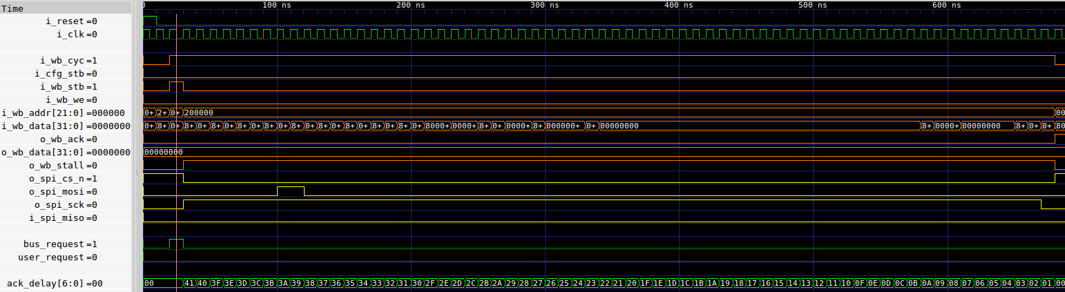 |
Fig 16 should look very much like our design requirement trace from Fig 12 above.
Now for the configuration port.
		initial	f_pending_user_request = 1'b0;
		always @(posedge i_clk)
		if ((i_reset)||(!i_wb_cyc))
			f_pending_user_request <= 1'b0;
		else if (user_request)
			f_pending_user_request <= 1'b1;
		else if (o_wb_ack)
			f_pending_user_request <= 1'b0;

		// The actual cover statement for the user request
		always @(posedge i_clk)
			cover((o_wb_ack)&&(f_pending_user_request));
The configuration trace this generates is shown below in Fig 17.
 |
Keep in mind, I’m able to acquire and examining these traces without writing any simulation code. That comes later, in a discussion we’ll need to save for another day.
Finally, to capture the pipelined read request, we’ll cover the entrance
into the pipeline read mode, just like we traced out in Fig. 13 above.
For this purpose, we can just cover() the lowered stall line when ack_delay
is one.
		if (OPT_PIPE)
		begin
			always @(posedge i_clk)
				cover((f_pending_bus_request)
					&&(ack_delay == 7'h1)
					&&(bus_request)&&(o_spi_sck));
The only problem is, the formal tools failed to find
any trace that would
make this cover() statement true. To debug that failed cover() statement,
I backed up a step, and tried to cover() the prior clock cycle.
			always @(posedge i_clk)
				cover((next_request)&&(f_pending_bus_request)
						&&(ack_delay == 7'h2));
		end
	end endgenerate
Eventually I get the trace in
Fig 18 from the first of these two cover() statements.
 |
This is also my general approach for those times where I am struggling to
get a cover() statement to produce a
trace: I back up a
step, add an additional cover() statement, and then repeat the process
until I find the bug–just like I showed here. assert() statements can help
this process as well.
Fig 18 also illustrates one of the problems with cover() statements: the tool
is free to cover your logic any way it pleases. In this case, it covered the
entrance into the pipelined read, and then immediately issued a
bus abort
by dropping the i_wb_cyc line. While legal, it’s hardly satisfying.
We could add some assumptions to keep this from taking place. That’s part of
the purpose of the F_OPT_COVER generate block–to be able to add any
assumptions necessary for getting the
traces you want. For example,
we could add an assumption that there would never be any
bus aborts during
pipelined reads. However, this cover() has accomplished my purpose as
it is: it has proven that a pipelined read request will bring the core
back into the regular read logic as desired. Therefore, I’ll leave any
further work with assumptions as a exercise for the student.
This helps me create an initial draft of this flash controller core. Well, not quite. I’ll describe a missing piece in the next section.
Step one: Reset and bus interaction
One of the problems with the cover() statements in the last section is that,
when unconstrained, the incoming bus request doesn’t act like a bus request
should. Bus requests may be made, stalled, and then new requests will be made
even though the prior request hasn’t gone been accepted into the
controller.
Similarly, the strobe line might be high, even though the bus cycle line is low.
For these reasons, we need to bring in some properties describing our
bus. Let’s do that in
this section, starting with the i_reset signal the
bus properties depend upon.
Reset logic uses the $past() operator. This operator will only work right
if the $past() time doesn’t occur before time began with the initial
statements. Hence, we’ll create an f_past_valid register to tell us when
we can use the $past() operator successfully.
	reg	f_past_valid;

	initial	f_past_valid = 1'b0;
	always @(posedge i_clk)
		f_past_valid <= 1'b1;
We want to assume() that our design starts with the i_reset line high.
This means we want to assume i_reset in both the initial state, and anytime
f_past_valid is false.
	initial	assume(i_reset);

	always @(*)
	if (!f_past_valid)
		assume(i_reset);
Now for a fun trick: I’d like to insure that any register responsive to an
i_reset signal is also properly initialized to the same value. Checking
for !f_past_valid tells us if we are in the initial state, whereas
$past(i_reset) checks whether or not our design just followed an
i_reset signal. By placing the asserted values below, that guarantees them
to be the same under both circumstances.
	always @(posedge i_clk)
	if ((!f_past_valid)||($past(i_reset)))
	begin
		assert(o_spi_cs_n == 1'b1);
		assert(o_spi_sck  == 1'b0);
		//
		assert(ack_delay    ==  0);
		assert(cfg_user_mode == 0);
		assert(o_wb_stall == 1'b0);
		assert(o_wb_ack   == 1'b0);
	end
Now we can start to get the Wishbone bus to act like a Wishbone bus should.
To do this, we’ll reference a Wishbone bus property file from the ZipCPU repository. This core needs a bit of configuration, so let’s configure its parameters:
-
AW: Our address bus has 22 bits, sufficient to handle a flash of 16MB of memory. (Remember the Wishbone address is a word address, and not an 8-bit octet address.) -
F_MAX_STALL: Our design may stall the bus no more than 66 clock cycles, one more than the length of one non-pipelined bus read. -
F_MAX_ACK_DELAY: Similarly, it may take at most 66 cycles for an acknowledgment to be returned upon any request.This is a bit of overkill for both
F_MAX_STALLandF_MAX_ACK_DELAYby one cycle, but it gives us a little wiggle room in case our design changes in the future. -
F_LGDEPTH: Since both counters require 7-bits, and since we’ll never have more than2^7or 128 requests outstanding, we’ll set the log (based two) of the pipeline depth to 7. This also determines the number of bits in our counters:f_nreqs, the number of requests that have been made,f_nacks, the number of acknowledgments that have been returned, andf_outstanding, the number of currently outstanding transactions. -
F_MAX_REQUESTSdescribes the maximum number of requests that can be made in any transaction. This creates an assertion thatf_nreqs < F_MAX_REQUESTS. While this is great for our non-pipelined mode, in the pipelined mode it is possible to make request upon request. Hence, we’ll set this to one for the non-pipelined mode, and to zero if we are running in a pipelined mode.
That’s enough configuration to include this property set in our design. We’ll
make one other adjustment here: we’ll OR the i_wb_stb and i_cfg_stb
together to create one unified slave port. This saves us from including two
separate property files to describe each of the two
Wishbone
slaves, but it’ll give us a bit of hassle that we’ll have to clean up in a moment.
	localparam	F_LGDEPTH = 7;
	wire	[F_LGDEPTH-1:0]	f_nreqs, f_nacks, f_outstanding;

	fwb_slave #( .AW(22), .F_MAX_STALL(7'd66), .F_MAX_ACK_DELAY(7'd66),
			.F_LGDEPTH(F_LGDEPTH),
			.F_MAX_REQUESTS((OPT_PIPE) ? 0 : 1'b1),
			.F_OPT_MINCLOCK_DELAY(1'b1)
		) slavei(i_clk, (i_reset),
		i_wb_cyc, (i_wb_stb)||(i_cfg_stb), i_wb_we,
			i_wb_addr, i_wb_data, 4'hf,
			o_wb_ack, o_wb_stall, o_wb_data, 1'b0,
			f_nreqs, f_nacks, f_outstanding);
Our first clean up assumption is to require that only one i_*_stb signal
will ever be active at any given time.
	always @(*)
		assume((!i_cfg_stb)||(!i_wb_stb));
Second, we’ll require that any time either of i_wb_stb or i_cfg_stb is
active, and the bus is stalled, that the same strobe signal remains active
on the next clock.
	always @(posedge i_clk)
	if ((f_past_valid)&&(!$past(i_reset))&&(i_wb_cyc)
		&&(($past(i_wb_stb))||($past(i_cfg_stb)))&&($past(o_wb_stall)))
		assume({i_wb_stb,i_cfg_stb}==$past({i_wb_stb,i_cfg_stb}));
In hindsight, this just makes sense. In reality, I didn’t put this assumption
into place until I saw this rule violated in one of my early cover()
traces.
Now that we’ve added our
bus properties,
the bus starts to act right in the
traces
generated by our cover() statements. The design just doesn’t pass
induction
yet. For that, we’ll need to add some ad-hoc assertions in the next section.
Step two: Ad-hoc Immediate assertions
Often I separate formal properties into two types: there’s the primary type based upon the outputs of the core that’s designed to determine whether the core functions as intended. We’ll call this the contract that the core needs to fulfill. Other properties are more ad-hoc. They wouldn’t be needed, save for the reality that induction starts with unconstrained values within the core. We’ll express how this core needs to operate, it’s contract if you will, using System Verilog sequences in the next section. For the purpose of this section, let’s just constrain the design to make certain it doesn’t enter into any illegal states during induction.
We’ll start out with some assertions regarding our
Wishbone properties.
Specifically, we need to ensure that the counters within the Wishbone property
module
match our current understanding of our state. Further, since a pipelined
operation can go on forever, we’ll only examine the number of outstanding
transactions kept in the f_outstanding value returned from the
Wishbone property set.
For our first test, we’ll insist that we never have more than one outstanding request. That is unless we are in a pipelined read operation, where there would be one cycle where the number of outstanding transactions would be two instead of one.
	always @(*)
	if (OPT_PIPE)
		assert(f_outstanding <= 2);
	else
		assert(f_outstanding <= 1);
In a similar fashion, any time ack_delay is zero then we aren’t in an
extended transaction. Such a time step must either include the o_wb_ack
from a just-ended transaction or the number of outstanding transactions
must be zero.
	always @(posedge i_clk)
	if (ack_delay == 0)
		assert((o_wb_ack)||(f_outstanding == 0));
Unfortunately, without anything more, we may get a
trace from the tools
that has o_wb_ack on for a very long time, yet f_outstanding is some value
inconsistent with our design. For example, the core could be responding to one
empty acknowledgment request after another while f_outstanding ==2.
Of course the core would never get into this situation, but we need to
communicate that to the
induction
engine.
In the first case, following any non-pipelined i_wb_stb request, there should
then be only one request outstanding.
	always @(posedge i_clk)
	if ((f_past_valid)&&(!i_reset)&&(i_wb_cyc))
	begin
		if (((!OPT_PIPE)||($past(o_spi_cs_n)))
			&&($past(i_wb_stb))&&(!$past(o_wb_stall))&&(i_wb_cyc))
			assert(f_outstanding == 1);
Likewise in the middle of any request, there should only be one bus request outstanding.
		if (ack_delay > 0)
			assert((o_wb_ack)||(f_outstanding == 1));
	end
If there are ever two acknowledgments back to back, they can only be the empty acknowledgments we discussed earlier. Hence, we should only have the last request outstanding or no requests outstanding.
	always @(posedge i_clk)
	if ((f_past_valid)&&(o_wb_ack)&&($past(o_wb_ack)))
		assert(f_outstanding <= 1);
There is only one time we should ever have two requests outstanding: that is
when we just accepted a request for a pipelined interaction and OPT_PIPE is
true. On that same clock, the acknowledgment line should be high, o_spi_cs_n
should be active (low), and ack_delay should be 32. Under no other
circumstances should there ever be two requests outstanding.
	always @(posedge i_clk)
	if (f_outstanding == 2)
		assert((OPT_PIPE)&&(o_wb_ack)&&(!o_spi_cs_n)&&(o_spi_sck)
			&&(ack_delay==7'd32));
Following any bus strobe that is neither a bus_request nor a user_request
of the configuration port, there should immediately be an acknowledgment
on the next clock.
	always @(posedge i_clk)
	if ((f_past_valid)&&($past(i_wb_stb))&&(!$past(o_wb_stall)))
	begin
		if ((i_wb_cyc)&&(!i_reset)
				&&(!$past(user_request))&&(!$past(bus_request)))
			assert((o_wb_ack)&&(f_outstanding == 1));
	end
That’s the last of the assertions necessary to make certain the formal properties for this core properly integrate with the properties from our Wishbone property set.
Now let’s make some assertions of the SPI protocol next.
If you’ve taken my course in formal verification, you may remember that I
usually spend some time discussing how to properly describe a
SPI
protocol interaction in the multi-clock section. This is not necessary
here. Not only is everything synchronous, but the
SPI interaction
of interest isn’t slow enough to make any of those multiclock property
descriptions, $rose(), $fell(), or $stable(), all that useful here.
Still, we can describe some useful parts of the interaction here.
For example, we’ve chosen to leave the clock idle unless o_spi_cs_n is low.
	always @(*)
	if (o_spi_cs_n)
		assert(!o_spi_sck);
While I suppose we could just leave the clock running, that would break some other things–notably the configuration port.
Similarly, any time ack_delay is other than zero, the SCK line should be
high. This would reference either o_spi_sck going to the output DDR
module,
or our local version of whether or SCK is really ticking in actual_sck.
	always @(*)
		assert((o_spi_sck||actual_sck) == (ack_delay > 0));
Anytime ack_delay is zero, we are not in the middle of any transactions.
Hence, o_wb_stall should also be zero.
	always @(*)
	if (ack_delay == 0)
		assert(!o_wb_stall);
Likewise, if the ack_delay is ever greater than one, then the bus should
be stalled.
	else if (ack_delay > 1)
		assert(o_wb_stall);
Indeed, with one exception any time ack_delay is greater than zero the bus
should be stalled. The one exception is just before a pipelined transaction.
Hence, if ack_delay is one and pipelined reads are disabled, or equivalently
if we are in the cfg_user_mode, then the interface should be stalled
when ack_delay is one.
	else if ((!OPT_PIPE)&&(ack_delay == 1))
		assert(o_wb_stall);
Just to constrain the
induction
engine further, the ack_delay should always be less than or equal to 65.
Although we know this to be true already, the
induction
engine can do some weird things if you don’t limit values like this properly.
	always @(*)
		assert(ack_delay <= 7'd65);
In a similar fashion, if cfg_user_mode is ever true, then the
ack_delay must be less than or equal to 9.
	always @(*)
	if (cfg_user_mode)
		assert(ack_delay <= 7'd9);
Our final ad-hoc assertion will be that o_spi_cs_n is only ever active
(low) if either we are in the cfg_user_mode or if ack_delay > 0.
	always @(*)
		assert(o_spi_cs_n != ((cfg_user_mode)||(ack_delay > 0)));
These simple assertions above will keep us in the valid operating range of this core. Now we just need to convince ourselves that this core actually works and does what it is supposed to do. To do that, we’ll try out some of the System Verilog sequences available to the Verific-enabled version of yosys.
Step three: Sequence Assertions
If you recall from the beginning of this article, one of the reasons for this project was to see if a flash controller would be a good test of System Verilog sequences. In particular, I’ve been looking for some of the use cases that highlight the utility of System Verilog’s sequences.
Prior to this project, I had only tested yosys’s ability to handle System Verilog sequences with FIFOs and a UART transmitter. Since starting this project, I have now tested and tried them out with a SPI-based ADC, and the SRAM controller for this same ICOZip Project. While I like the expressiveness of the System Verilog sequence language, I’m also glad I learned how to do formal verification with immediate assertions only first. Sequence are not nearly as simple or as easy to work with as the immediate assertions we’ve been working with, and the background I gained in immediate assertions helped me a lot while learning sequences.
We’ll split the
sequences
discussion here into two parts. The first part, contained in this section,
will be about guaranteeing that our ack_delay based state machine works as
desired. In the next section, will dig in a bit further and verify that what
gets returned to the bus is actually what we read from the device. Once we’re
done, we’ll move on to how I tested this
core
on the actual hardware of the ICO board.
In many ways, it might make the most sense to read this section from the bottom up, rather than the top down, because in order to finally express what we want to at the end, we have to build a lot of infrastructure to get there. Hence, if you want to see where we are going, skip to the end of this section and look over the assertions found there.
That said, let’s start with two variables these sequences will use. In particular, we want some values that are guaranteed to stay constant throughout the duration of the sequences–values the sequences can reference, and that won’t change. We’ll create two here, one to capture the last address requested of the bus, and a second to capture what would be the next address after that.
`ifdef	VERIFIC
	reg	[21:0]	f_last_addr, f_next_addr;

	always @(posedge i_clk)
	if (bus_request)
		f_last_addr <= i_wb_addr[21:0];

	always @(*)
		f_next_addr <= f_last_addr + 1'b1;
Our first assertion is something simple: Any request, other than a
user_request (i.e. a write) of the configuration port or a normal
bus_request (i.e. a read) should be acknowledged on the next clock, without
stalling the bus.
	assert property (@(posedge i_clk)
		disable iff ((i_reset)||(!i_wb_cyc))
		((i_wb_stb)||(i_cfg_stb))&&(!o_wb_stall)
				&&(!user_request)&&(!bus_request)
		|=> (o_wb_ack)&&(!o_wb_stall));
If this form of an assertion is new to you, then don’t let it be. We’ve been discussing this basic assertion for some time, only we’ve described it in a different fashion. Instead of,
	assert property (@(posedge i_clk)
		A |=> B);
we’ve been writing
	always @(posedge i_clk)
	if ((f_past_valid)&&($past(A)))
		assert(B);
The two are really just two forms of the same thing. Personally, I like the new form. It seems simpler and cleaner.
What about the disable iff statement? That just disables the assertion
on any of the clocks that it would be applied to. Hence,
	assert property (@(posedge i_clk)
		disable iff (C)
		A |=> B);
is the same as
	always @(posedge i_clk)
	if ((f_past_valid)&&($past(A))&&(!$past(C))&&(!C))
		assert(B);
There’s another new form as well. Instead of writing,
	always @(*)
	if (A)
		assert(B);
we could equivalently write
	assert property (@(posedge i_clk)
		A |-> B);
Both of these newer forms, however, currently require the Verific enabled version of yosys.
Using this newer form, I can express
	assert property (@(posedge i_clk)
		(i_wb_stb)&&(!o_wb_stall)&&(!o_spi_cs_n)&&(!i_wb_we)
			&&(!cfg_user_mode)
		|-> (OPT_PIPE)&&(i_wb_addr == f_next_addr)
		);
That is to say, if we ever accept a new bus_request while o_spi_cs_n
is active (low), then OPT_PIPE must be valid and this new request
address must be for the next address in the
flash.
Those two assertions should get your feet wet. Now let’s try our first sequence. If you’ve never used them, sequences are neither assertions nor assumptions. Instead, they can be used to describe a sequence of states that can then be used within an assertion, assumption, or even a cover property.
For this first sequence, let’s describe the
flash
read command where we send a 8'h03 to the
flash
device. This sequence starts with an idle cycle with o_spi_cs_n active
and o_spi_sck true, but actual_sck hasn’t been set yet.
We’ll start this description by naming our
sequence,
READ_COMMAND.
	sequence READ_COMMAND;
		// Send command 8'h03
Then we’ll describe that first state.
		(f_last_addr == $past(i_wb_addr))
				&&(!o_spi_cs_n)&&(o_spi_sck)&&(!o_spi_mosi)
				&&(!actual_sck)
On the next clock, we get into sending the actual command contained in the
o_spi_mosi output values. To express that this will start on the next
clock, we’ll use the ##1 expression. This portion of the
sequence,
however, will take us a whole 8 clocks. During all of those 8 clocks,
we’ll want to assert that the f_last_addr value stays constant, that
o_spi_cs_n stays active, and that o_spi_sck remains true. Hence,
throughout these next 8-clocks, these must hold. That’s the purpose of
the throughout statement.
		##1 ( ((f_last_addr == $past(f_last_addr))
			&&(!o_spi_cs_n)&&(o_spi_sck)&&(actual_sck)) throughout
Now we can work our way through each of those individual 8 clocks.
				(!o_spi_mosi)&&(ack_delay==7'd64)&&(actual_sck)
				##1 (!o_spi_mosi)&&(ack_delay==7'd63)
				##1 (!o_spi_mosi)&&(ack_delay==7'd62)
				##1 (!o_spi_mosi)&&(ack_delay==7'd61)
				##1 (!o_spi_mosi)&&(ack_delay==7'd60)
				##1 (!o_spi_mosi)&&(ack_delay==7'd59)
				##1 ( o_spi_mosi)&&(ack_delay==7'd58)
				##1 ( o_spi_mosi)&&(ack_delay==7'd57));
	endsequence
In this
sequence
description, I’ve tried to constrain and describe every register that’s a part
of state associated with sending this command. Further, since the o_spi_mosi
and ack_delay values changed during these 8-clocks, I didn’t lump them
together with the other predicates that needed to be true throughout
all eight of these cycles.
The next sequence is the one where we send the address we want to read from to the SPI flash. Since the Wishbone bus is word based, and the flash is byte based, we’ll add two zero’s at the end of this sequence. The format itself should look very similar to the format of the last one: we’ll start by naming the sequence,
sequence SEND_ADDRESS;then we’ll define those properties that must hold throughout the sequence,
		(((f_last_addr == $past(f_last_addr))&&(!o_spi_cs_n)&&(o_spi_sck)
			&&(actual_sck))
		throughout
finally, we’ll step through each of the clock cycles within the sequence.
			(o_spi_mosi == f_last_addr[21])&&(ack_delay==7'd56)
			##1 (o_spi_mosi == f_last_addr[20])&&(ack_delay==7'd55)
			##1 (o_spi_mosi == f_last_addr[19])&&(ack_delay==7'd54)
			##1 (o_spi_mosi == f_last_addr[18])&&(ack_delay==7'd53)
			##1 (o_spi_mosi == f_last_addr[17])&&(ack_delay==7'd52)
			##1 (o_spi_mosi == f_last_addr[16])&&(ack_delay==7'd51)
			##1 (o_spi_mosi == f_last_addr[15])&&(ack_delay==7'd50)
			##1 (o_spi_mosi == f_last_addr[14])&&(ack_delay==7'd49)
			##1 (o_spi_mosi == f_last_addr[13])&&(ack_delay==7'd48)
			##1 (o_spi_mosi == f_last_addr[12])&&(ack_delay==7'd47)
			##1 (o_spi_mosi == f_last_addr[11])&&(ack_delay==7'd46)
			##1 (o_spi_mosi == f_last_addr[10])&&(ack_delay==7'd45)
			##1 (o_spi_mosi == f_last_addr[ 9])&&(ack_delay==7'd44)
			##1 (o_spi_mosi == f_last_addr[ 8])&&(ack_delay==7'd43)
			##1 (o_spi_mosi == f_last_addr[ 7])&&(ack_delay==7'd42)
			##1 (o_spi_mosi == f_last_addr[ 6])&&(ack_delay==7'd41)
			##1 (o_spi_mosi == f_last_addr[ 5])&&(ack_delay==7'd40)
			##1 (o_spi_mosi == f_last_addr[ 4])&&(ack_delay==7'd39)
			##1 (o_spi_mosi == f_last_addr[ 3])&&(ack_delay==7'd38)
			##1 (o_spi_mosi == f_last_addr[ 2])&&(ack_delay==7'd37)
			##1 (o_spi_mosi == f_last_addr[ 1])&&(ack_delay==7'd36)
			##1 (o_spi_mosi == f_last_addr[ 0])&&(ack_delay==7'd35)
Don’t forget the two zero bits at the end of the address!
			##1 (o_spi_mosi == 1'b0)&&(ack_delay==7'd34)
			##1 (o_spi_mosi == 1'b0)&&(ack_delay==7'd33));
	endsequence
We can now define a third
sequence:
the one where we actually read the data from the device. This has the exact
same form as before, only we’re going to introduce new expression, the [*8]
or [*7]. This means that we want to repeat the given state by that many
clocks. I’m going to use this to help keep ack_delay bounded–at least
bounded enough that the formal tools properly recognize after more than eight
clocks which state of this sequence is taking place, should they decide
to try to start in the middle of the
sequence.
As before, we start with the name of the
sequence
followed by the properties that will hold throughout the
sequence.
	sequence	READ_DATA;
		(((o_wb_stall)&&(!o_spi_cs_n)&&(o_spi_sck)
			&&(o_wb_data == $past({o_wb_data[30:0], i_spi_miso})))
		throughout
The first clock period, however, will be replicated 8 times. It will primarily
just constrain ack_delay.
(ack_delay <= 7'd32)&&(ack_delay >= 7'd25) [*8]And so on, repeating each clock period 8 times until the last.
		##1 (ack_delay <= 7'd24)&&(ack_delay >= 7'd17) [*8]
		##1 (ack_delay <= 7'd16)&&(ack_delay >=  7'd9) [*8]
		##1 (ack_delay <=  7'd8)&&(ack_delay >=  7'd2) [*7])
Watch the parentheses, because that last line also ends the throughout
statement that we started with, even though the we’re not done defining
this
sequence
yet.
We’ve broken the
sequence
at this point because the next period is special.
That’s the only period where the our signals might change in order to support
a pipelined interaction. In this case, the stall line might be low if
OPT_PIPE is also true, otherwise we remain stalled like we were in the
last clock.
		##1 ((!o_spi_cs_n)&&(actual_sck)&&(ack_delay == 7'd1)
			&&(((OPT_PIPE)&&(i_wb_stb)&&(!i_wb_we)&&(o_spi_sck))
				||((o_wb_stall)&&(!o_spi_sck)))
			&&(o_wb_data == $past({o_wb_data[30:0], i_spi_miso})))
Finally, we’ll end this
sequence
describing a read from the
flash memory
with a bus acknowledgment, and a guarantee if OPT_PIPE isn’t true
that the bus has returned to idle.
		##1 (o_wb_ack)
			&&(o_wb_data == $past({o_wb_data[30:0], i_spi_miso}))
			&&((OPT_PIPE)||((o_spi_cs_n)
					&&(!o_spi_sck)&&(!actual_sck)));
	endsequence
What can you do with all these sequence we’ve just defined? You can string them together within an assertion!
The following assertion asserts that, following any read request from the
Wishbone bus,
the device will send the READ_COMMAND, the address (SEND_ADDRESS), and
then read the data (READ_DATA) from the device.
	assert property (@(posedge i_clk)
		disable iff ((i_reset)||(!i_wb_cyc))
		(i_wb_stb)&&(!o_wb_stall)&&(!i_wb_we)&&(o_spi_cs_n)
			&&(!cfg_user_mode)
		// Send command 8'h03
		|=> READ_COMMAND
		// Send the requested address
		##1 ((f_last_addr == $past(f_last_addr)) throughout
				SEND_ADDRESS)
		// Clock in 32-bits of data
		##1 READ_DATA);
Not bad, huh?
This gets us most of the way there. However, a flash is a type of memory, and there are particular properties you want to formally verify with respect to any memory interaction. That will be our next section.
Step four: Known Address/Data Assertions
The rule for formally verifying memories is that you want to assume any time you read from an arbitrary address, that you get a known arbitrary value in response. The second part is to assert that whenever you return the result of the read to the bus, you also return the arbitrarily chosen value.
I initially created those rules here in
sequence
logic. One property assumed known data would be read from i_spi_miso
following a request from that known address, and the second property asserted
that the same known data would be returned in o_wb_data once o_wb_ack was
set.
I’ve since torn that work up. It turns out that there’s an easier way to do the same thing when you are using sequences. We’ll still allow the formal tool to pick an arbitrary data value, but we can do this without the heavy weight of the formal memories rule. In particular, we don’t need the arbitrary address, just the data.
Here’s how we’ll do it: we’ll create a rule that whenever the arbitrary data is read, regardless of what address it is read from, that value read from the device is returned to the bus.
We’ll start at the top by assuming a constant 32-bit value. The formal solver will get to pick any value it wants for these 32-bits.
(* anyconst *) wire [31:0] f_data;Next, we’ll define a
sequence
where an arbitrary octet, B, is received from the interface.
	sequence	DATA_BYTE(local input [7:0] B);
		(i_spi_miso == B[7])
		##1 (i_spi_miso == B[6])
		##1 (i_spi_miso == B[5])
		##1 (i_spi_miso == B[4])
		##1 (i_spi_miso == B[3])
		##1 (i_spi_miso == B[2])
		##1 (i_spi_miso == B[1])
		##1 (i_spi_miso == B[0]);
	endsequence
Did you notice that this sequence accepted an 8-bit parameter? Neat!
Now, if we string four of these
sequence
together, then we can describe receiving an arbitrary value on the i_spi_miso
wire.
	sequence	THIS_DATA;
			DATA_BYTE(f_data[31:24])
			##1 DATA_BYTE(f_data[23:16])
			##1 DATA_BYTE(f_data[15: 8])
			##1 DATA_BYTE(f_data[ 7: 0]);
	endsequence
Note that this only works because f_data is constant, since the
sequence
will reference the current value of f_data, rather than the value
when the
sequence
is activated.
Now, here’s the trick: THIS_DATA is a
sequence
containing a description of our known data being received. While this
sequence
is being received, ack_delay will go from 7'd32 down to 7'd1. Once
ack_delay hits zero, or goes around again, there should also be an
acknowledgment. So, let’s add to that assertion that the outgoing data also
matches the received data.
	assert property (@(posedge i_clk)
		(THIS_DATA and ((!i_reset)&&(i_wb_cyc)
			throughout
		((ack_delay == 7'd32)
			##1 (ack_delay == $past(ack_delay)-1) [*31])))
		|=> (o_wb_ack)&&(o_wb_data == f_data));
Did you see how this accomplishes both sides of the
memory proof
requirement? Because we placed the
known data
sequence
before the non-overlapping implication operator, |=>, the
sequence
acted as an assumption. As a result, we now know that no matter what
value is received, the proper value will be returned.
I then applied the same basic approach to the configuration port. However, in the interests of space in an already long article, I’ll let you peruse it if you are interested.
	generate if (OPT_CFG)
	begin
		// Configuration writes
		assert property (@(posedge i_clk)
			disable iff ((i_reset)||(!i_wb_cyc))
			((i_cfg_stb)&&(!o_wb_stall)&&(i_wb_we)&&(i_wb_data[8]))
			|=> ((!cfg_user_mode)&&(o_spi_cs_n)&&(!o_spi_sck))
				&&(o_wb_ack)&&(!o_wb_stall));

		reg	[7:0]	f_wr_data;
		always @(posedge i_clk)
		if (user_request)
			f_wr_data <= i_wb_data[7:0];

		assert property (@(posedge i_clk)
			disable iff ((i_reset)||(!i_wb_cyc))
			((i_cfg_stb)&&(!o_wb_stall)&&(i_wb_we)&&(!i_wb_data[8]))
			|=> (((cfg_user_mode)&&(!o_spi_cs_n)&&(o_spi_sck)
				&&(o_wb_stall)) throughout
				(!o_spi_mosi)&&(ack_delay==7'd9)
				##1 (o_spi_mosi == f_wr_data[7])
							&&(ack_delay==7'd8)
				##1 (o_spi_mosi == f_wr_data[6])
							&&(ack_delay==7'd7)
				##1 (o_spi_mosi == f_wr_data[5])
							&&(ack_delay==7'd6)
				##1 (o_spi_mosi == f_wr_data[4])
							&&(ack_delay==7'd5)
				##1 (o_spi_mosi == f_wr_data[3])
							&&(ack_delay==7'd4)
				##1 (o_spi_mosi == f_wr_data[2])
							&&(ack_delay==7'd3)
				##1 (o_spi_mosi == f_wr_data[1])
							&&(ack_delay==7'd2))
			##1 ((cfg_user_mode)&&(!o_spi_cs_n)&&(!o_spi_sck)
				&&(actual_sck)&&(o_wb_stall)
				&&(o_spi_mosi == f_wr_data[0])
							&&(ack_delay==7'd1))
			##1 (o_wb_ack)&&(!o_wb_stall)&&(cfg_user_mode)
				&&(!o_spi_sck)&&(!actual_sck)&&(!o_wb_stall));

		// And then configuration reads.  First the write needs to
		// charge the o_wb_data buffer
		assert property (@(posedge i_clk)
			disable iff ((i_reset)||(!i_wb_cyc))
			((i_cfg_stb)&&(!o_wb_stall)&&(i_wb_we)&&(!i_wb_data[8]))
			##2 DATA_BYTE(f_data[7:0])
			|=> (o_wb_ack)&&(o_wb_data == { 24'h0, f_data[7:0] })
				&&(cfg_user_mode)&&(!o_wb_stall));

		// Then it needs to stay constant until another SPI
		// command
		assert property (@(posedge i_clk)
			disable iff (i_reset)
			($past(!o_spi_sck))&&(!o_spi_sck)&&(cfg_user_mode)
			|=> $stable(o_wb_data)&&(o_wb_data[31:8]==0));

	end endgenerate
How to test it?
Now that we’ve built our controller, how shall we test it to know that it works?
Hopefully you’ve been around long enough to remember all of our work building a basic debugging bus, following the initial vision I presented for controlling FPGA logic. With just a little effort, we can connect a Wishbone scope and our flash controller to this debugging bus, and then see how our flash interacts with the FPGA.
 |
For this particular core,
I didn’t start my debugging with the
Wishbone
scope.
I started instead with a Digilent Digital
Discovery 2.
Why? Two reasons: 1. I had it available to
me
and on my desk, and 2. I was concerned about the timing of the clock pulses.
Sure enough, the
DD
revealed that the
iCE40
SB_IO primitive in DDR mode delayed the SCK by one clock more than I was
expecting. (The code above has been fixed to accommodate this.) This sent
me back through the entire design to do some massive updates:
all other signals needed to be delayed by one and the o_spi_sck signal
needed to return to zero one cycle earlier. Indeed, there were several head
scratching moments at this point in order to get the timing right.
We’ve discussed hooking up the Wishbone scope to a design before. I’ll just touch on a couple of pieces briefly here. First, you need to decide which 32-bits you want to capture and select a relevant trigger. I personally like to place the trigger in the MSB of this word–it makes it easier to switch to a compressed wishbone scope later if I need to. In my case, I ultimately chose the following wires to capture:
	assign	spixpress_debug = { (!o_spi_cs_n), wb_cyc,
				(wb_stb)&&(flash_sel),
				(wb_stb)&&(flash_cfg_sel), wb_we,
				flash_stall,flash_ack, wb_data[8:0],
				flash_data[8:0],
				3'h0,
				o_spi_cs_n, o_spi_sck, o_spi_mosi, i_spi_miso };
That gives me access to all of the critical Wishbone wires, as well as the entire SPI interface.
The majority of the connections required to connect this to the Wishbone bus were made by AutoFPGA–allowing me to remove the scope later if I so wish by just removing the scope’s AutoFPGA configuration file’s name from the AutoFPGA command line. Among other changes, this places the following additional code into the main design file of this design.
	wbscope #(.LGMEM(7), .SYNCHRONOUS(1), .HOLDOFFBITS(8))
		spixscopei(i_clk, 1'b1, (!o_spi_cs_n), spixpress_debug,
			i_clk, wb_cyc, (wb_stb)&&(spixscope_sel),
			wb_we, wb_addr[0], wb_data,
			spixscope_ack, spixscope_stall, spixscope_data,
			spixscope_int);
The AutoFPGA configuration
file
also places a #define into the
regdefs.h
file, defining R_SPIXSCOPE to have the address of the control
register for the
scope.
You can see the entire AutoFPGA configuration file for this debugging scope here. Adding this to the AutoFPGA command line in the auto-data/Makefile will add this to the design, and removing it from the command line will remove this component and all of its dependencies from the design as well. There’s also a software component to this scope’s setup as well, found in the sw/host directory of the project—but we’ve discussed how to build those before.
Test one: Using wbregs to read a known value from the flash
The next step, and really the first true test, is an important one when designing for an FPGA: you want to make certain you can read back a known piece of data from the FPGA. While there may be other uses for the vendor identification protocol within the flash specification, I find that using it as a test read from the device is the most useful. In particular, if I read that ID from the flash, I can quickly determine if I managed to get the sequencing right between all of the various signals.
Looking over the flash
specfication,
you’ll see that sending a 0x9f to the
flash
chip will request this identification value. Ever after until the chip select
is deactivated, the incoming data to the
flash is ignored, and the
outgoing data from the flash
will be this known identification sequence–just as we showed in Fig. 14 above.
Most of my designs contain a command-line driven
peek and poke
capability I call
wbregs.
This command,
found in almost all of my system-level
projects, allows you to read or
write addresses within the device’s internal
Wishbone bus,
just the same as though those commands were issued
internally from a source within the design.
In this project, which needs to support
software on both the Raspberry
Pi and on whatever host machine might connect
to it, the
project will build one of two versions of this
wbregs
program. The first is arm-wbregs for running on the
Pi, whereas the second is pc-wbregs for
running on whatever other host platform might connect with the
Pi over a TCP/IP
connection.
Let’s run this flash manufacture
identification test using pc-wbregs.
$ ./pc-wbregs flashcfg 0x0100
00200000 (FLASHCFG)-> 00000100
$ ./pc-wbregs flashcfg 0x09f
00200000 (FLASHCFG)-> 0000009f
$ ./pc-wbregs flashcfg 0x000 ; ./pc-wbregs flashcfg
00200000 (FLASHCFG)-> 00000000
00200000 (FLASHCFG) : [....] 00000001
$ ./pc-wbregs flashcfg 0x000 ; ./pc-wbregs flashcfg
00200000 (FLASHCFG)-> 00000000
00200000 (FLASHCFG) : [....] 00000020
$ ./pc-wbregs flashcfg 0x000 ; ./pc-wbregs flashcfg
00200000 (FLASHCFG)-> 00000000
00200000 (FLASHCFG) : [....] 00000018
$ ./pc-wbregs flashcfg 0x000 ; ./pc-wbregs flashcfg
00200000 (FLASHCFG)-> 00000000
00200000 (FLASHCFG) : [...M] 0000004d
$ ./pc-wbregs flashcfg 0x000 ; ./pc-wbregs flashcfg
00200000 (FLASHCFG)-> 00000000
00200000 (FLASHCFG) : [....] 00000001
$ ./pc-wbregs flashcfg 0x000 ; ./pc-wbregs flashcfg
00200000 (FLASHCFG)-> 00000000
00200000 (FLASHCFG) : [....] 00000080
$ ./pc-wbregs flashcfg 0x000 ; ./pc-wbregs flashcfg
00200000 (FLASHCFG)-> 00000000
00200000 (FLASHCFG) : [...1] 00000031
$ ./pc-wbregs flashcfg 0x000 ; ./pc-wbregs flashcfg
00200000 (FLASHCFG)-> 00000000
00200000 (FLASHCFG) : [...0] 00000030
$ ./pc-wbregs flashcfg 0x000 ; ./pc-wbregs flashcfg
00200000 (FLASHCFG)-> 00000000
00200000 (FLASHCFG) : [....] 00000083
$ ./pc-wbregs flashcfg 0x000 ; ./pc-wbregs flashcfg
00200000 (FLASHCFG)-> 00000000
00200000 (FLASHCFG) : [....] 000000ff
If you watched the lower octet of the results, you’ll see that we just
read the ID string: 01:20:18:4d:01:80:31:30:83. While that works for
debugging by hand, it’s somewhat hard to read and we can do this better. So
let’s tighten this up a bit, by switching our development to C++.
Test two: Accessing the flash from within a C++ program
I thought it might be fun to show how easy this is to do via C++ when using
the debugging bus concept.
When using the debugging bus
interface,
all it takes is a call to the m_fpga->readio(addr); method to read from the
FPGA, or
likewise a m_fpga->writeio(addr,value); call to write a value to the
FPGA. In our
case, we have a configuration register at address R_FLASHCFG that we wish
to read from or write to, so an example of reading from this register would
look like,
val = m_fpga->readio(R_FLASHCFG);Looking at the relevant portion of flashid.cpp, it starts with clearing
the trigger for the
scope
(if present).
#ifdef	R_SPIXSCOPE
	// Start up the scope at the beginning, in case anything goes wrong
	m_fpga->writeio(R_SPIXSCOPE, 124);
#endif
This will cause the
scope
to trigger on the lowering of the CS_n line, and then to wait another
124 clocks before it freezes its buffer and stops
collecting.
The next step is to issue the READID command (0x9f) to the
flash.
m_fpga->writeio(R_FLASHCFG, 0x09f);This will send a 0x9f to the
flash, and leave the chip select
active–just the way we designed this
core to
behave above.
We can now read the actual identification bytes. Even though our goal is to read, because of how we built the interface we’ll need to write to the register first in order to clock the data out out of the device. The information we write isn’t relevant, so we can just write a zero, and later read from the register.
The following does exactly that, but with perhaps a little more flair.
	m_fpga->writeio(R_FLASHCFG, 0x000);
	printf("ID:");
	for(int i=0; i<12; i++) {
		unsigned	id;

		// Read and print the last byte read
		id = m_fpga->readio(R_FLASHCFG);
		printf("%c%02x", (i==0)?' ':':', id&0x0ff);
		// and clock in the next byte across the SPI interface
		m_fpga->writeio(R_FLASHCFG, 0x000);
	} printf("\n");
Finally, now that we are all done, we’ll want to return the flash to its default state, allowing regular reads to be made again.
m_fpga->writeio(R_FLASHCFG, 0x100);What happens when we run this program?
$ ./pc-flashid
ID: 01:20:18:4d:01:80:31:30:83:ff:ff:ff
This is essentially the same thing we did before with pc-wbregs, only now
done from within C++. That looks prettier now, doesn’t it?
If you look this value up in the flash specification, you can verify that these are indeed the right values we should expect. Therefore, we’ve now finished test number two.
Test three: Copying the memory out of the flash
For our next test, let’s try reading from the flash.
We could use wbregs again to read a word from the
flash. Here we read the
first word from the flash.
$ ./pc-wbregs flash
01000000 (   FLASH) : [....] ff0000ff
This looks like a synchronization word. Indeed, it matches the first word in our binary design file, suggesting this might also be the first word of the binary that came shipped with our ICO board.
So … let’s read out the entire design!
We’ll do that with a program I call
dumpflash.
It’s usually the first program I run on any board I purchase, so that I never
lose the original manufacture provided pre-loaded design image. The relevant
line to read the entire flash,
found within
`dumpflash.cpp,
is simply
m_fpga->readi(DUMPMEM, BUFLN, buf);That’s it! By the time that command returns, and it will take a while since
it’s reading the ENTIRE flash
memory, the DUMPMEM buffer
will contain all of the contents from the
flash.
Not all of these contents are relevant.
When a flash is erased, all of the bits within it are set to ones. Usually, upon delivery, this is how a flash comes from the manufacturer with one exception: the board manufacturer has usually placed an initial load into the beginning of the flash memory. For this reason, we can trim any all one’s words from the end of the flash image.
	sz = BUFLN-1;
	while((sz>0)&&(buf[sz] == 0xffffffff))
		sz--;
	sz+=1;
Once done, we can write the flash contents to an external file.
	fp = fopen(fname,"w");
	if (fp == NULL) {
		fprintf(stderr, "ERR: Could not write %s\n", fname);
		exit(EXIT_FAILURE);
	}
	fwrite(buf, sizeof(buf[0]), sz, fp);
	fclose(fp);
That was easier than you might have expected, now, wasn’t it? See how powerful the debugging bus concept is?
Just as a foot note, be aware that this data may be byte swapped at this point. The debugging bus implementation I’ve created is big endian, even though most computers these days are little endian.
Test four: Writing to the flash
Each of the projects I have containing a flash chip also contains a flash driver host software component. This makes writing to the flash fairly simple.
The C++ interface
to this device driver
is primarily a simple write function.
class	FLASHDRVR {
	// ...
	FLASHDRVR(DEVBUS *fpga) : m_fpga(fpga) { m_debug = true; }
	// ...
	bool	write(const unsigned addr, const unsigned len,
			const char *data, const bool verify=false);
};
By calling this function with the address within the flash that you wish to write to, together with the length of the data and a pointer to that same data, the device driver will first check what is currently written on the flash, erase if necessary, and then write the new values to the flash.
That function calls two other functions that need to work in order to be able
to program and reprogram the
flash. The
first is the erase_sector function, and the second the page_program
function. Sector in this context is 4kB
of flash memory,
aligned on a 4kB boundary. A page is similar: it references
256 bytes of memory, aligned on a 256 byte boundary.
Erasing a sector requires a couple steps. First, a command needs to sent to the
flash
to enable write mode. This is a simple 8'h06 command that needs to be sent
to the flash.
It’s a straight forward use of the configuration port. We’ll start by
clearing the configuration mode by writing 9'100 to the interface, just out
of an abundance of caution to make certain o_spi_cs_n is high (inactive).
We’ll then write the 8'h06 write enable command, F_WREN, and tell
the
controller
to end the transaction by lowering o_spi_cs_n again.
	// Write enable
	m_fpga->writeio(R_FLASHCFG, F_END);
	m_fpga->writeio(R_FLASHCFG, F_WREN);
	m_fpga->writeio(R_FLASHCFG, F_END);
We can now issue the sector erase command, F_SE or 0x0d8. This command
is followed by a three byte argument containing the
address of the 4kB segment that we wish to erase.
	m_fpga->writeio(R_FLASHCFG, F_SE);
	m_fpga->writeio(R_FLASHCFG, (flashaddr>>16)&0x0ff);
	m_fpga->writeio(R_FLASHCFG, (flashaddr>> 8)&0x0ff);
	m_fpga->writeio(R_FLASHCFG, (flashaddr    )&0x0ff);
	m_fpga->writeio(R_FLASHCFG, F_END);
We’ll then wait for this operation to complete by calling flwait().
This function simply sends the “read-status register” command, F_RDSR1=0x05,
to the flash. Ever after, every time 8-clocks are sent to the flash an
updated status register will be returned. Once the low order bit, WIP=1,
is clear, the flash has finished erasing our sector.
void	FLASHDRVR::flwait(void) {
	const	int	WIP = 1;	// Write in progress bit
	DEVBUS::BUSW	sr;

	m_fpga->writeio(R_FLASHCFG, F_END);
	m_fpga->writeio(R_FLASHCFG, F_RDSR1);
	do {
		m_fpga->writeio(R_FLASHCFG, F_EMPTY);
		sr = m_fpga->readio(R_FLASHCFG);
	} while(sr&WIP);
	m_fpga->writeio(R_FLASHCFG, F_END);
}
Erasing a sector turns all the bits in that sector to 1. This really isn’t
what we want to do end the end. We want our data written to the flash,
regardless of whether it consists of 1’s or 0’s, and we want the 1’s
and 0’s put in the right place. The difference is associated with how
flash is built. The only way to turn a bit from a 0 to a 1 is to first erase a large block of flash
memory. In this case, we erased
a 4kB sector. Some
flash chips allow erasing smaller
portions of memory called subsectors.
One problem that results from erasing 4kB at a time in order to write to flash memory is that of collateral damage: it is possible that by erasing a sector, some other valuable information in that sector will get erased. This flash driver handles that problem by assuming that you will be smart enough not to do that. (You will, right?) If you write to the flash using this driver, starting from a sector boundary and ending on a sector boundary then you will have no problems.
The second step of writing information to a
flash is to program the
flash memory. Programming the
flash turns user specified bits
to 0. It cannot return bits to 1, it can only turn them from 1 to 0.
Programming the flash is, in many ways, very similar to the erase cycle presented above. It starts with sending a write enable command to the flash,
		// Write enable
		m_fpga->writeio(R_FLASHCFG, F_END);
		m_fpga->writeio(R_FLASHCFG, F_WREN);
		m_fpga->writeio(R_FLASHCFG, F_END);
followed by a “page program” command, F_PP = 0x02 to actually write
the page of flash memory.
		// Issue the command
		m_fpga->writeio(R_FLASHCFG, F_PP);
Like the erase command, the page program command needs the address of where to begin programming. This is passed as a three byte argument following the 8-bit command word.
		// The address
		m_fpga->writeio(R_FLASHCFG, (flashaddr>>16)&0x0ff);
		m_fpga->writeio(R_FLASHCFG, (flashaddr>> 8)&0x0ff);
		m_fpga->writeio(R_FLASHCFG, (flashaddr    )&0x0ff);
The third step is to write the data, byte by byte, to the flash controller, and hence to the flash chip.
		// Write the page data itself
		for(unsigned i=0; i<len; i++)
			m_fpga->writeio(R_FLASHCFG, data[i] & 0x0ff);
		m_fpga->writeio(R_FLASHCFG, F_END);
	// ...
Once this programming request closes, the flash
will become busy again. As with the erase, we’ll call the flwait()
function to wait for the flash to complete.
Now, using the zipload program, we can load a ZipCPU executable program onto the flash, to see if it runs.
I’ll skip to the end at this point and just say that the interface works. You can now run the ZipCPU CPUTEST on the ICO board. Hello World works too!
If you’d like more instructions, feel free to check out the README to the icozip project.
Conclusion
Okay, so what have we done here?
-
We learned about basic SPI interactions.
-
We’ve built a flash controller to get fast access to reading from the flash, quick access to continued readings, and we even created a configuration port for issuing arbitrary commands to the flash.
-
We demonstrated how a
cover()statement can make building a new core easier. -
We learned about System Verilog sequences, and saw how they could simplify properties describing interactions that take place over several clock cycles.
-
We looked at how the memory properties for reading the flash could be written with just a single assertion.
-
We then saw how powerful the debugging bus was in order to know if this device driver worked or not.
-
Finally, I pointed you to instructions for running one of two demonstration programs on the ZipCPU on the ICO board.
That’s a lot of ground in one post! However, notice how it was necessary to make it from design to demonstration to know that the flash controller fully worked.
While this may be a first flash controller, I wouldn’t recommend stopping here. Most flash chips offer DSPI or QSPI support, and even then there’s an eXecute In Place (XIP) option on top of that. Usually, for a flash controller, XIP means that you don’t need to re-issue the command–you can just issue the address and start reading. However, these are topics we may return to on another day, but until then I would encourage you to look into on your own should you be so interested.
For I am the LORD, I change not; therefore ye sons of Jacob are not consumed. (Malachi 3:6)