
Formally Verifying Asynchronous Components
To date, our formal verification efforts have primarily centered around synchronous designs using yosys, that is those designs where all logic transitions on the same clock edge, rather than looking at asynchronous designs. The one exception so far has been the description of how to get an asynchronous reset to pass induction. I’d like to move beyond this simple example towards verifying a full asynchronous FIFO design, but that’s going to require a bit more background in how to formally verify an asynchronous design in general. Today, therefore, let’s examine how to formally verify an asynchronous component that crosses between clock domains.
If you aren’t familiar with formal verification, you might wish to go back and review our introductory article on the topic. You might also find the induction exercise to be valuable as well.
 |
Today, let’s demonstrate how these same formal verification concepts apply an asynchronous design with two clocks within it. In this case, we’ll examine a clock switch. Such a switch takes two clock inputs and one line to select between them. In our case, the two separate clocks makes a perfect example of how formal methods can be applied to an asynchronous design.
Two Clocks
The first and most important step is to somehow describe both clocks via formal properties to the SMT solver. This step is really independent of anything you might wish to verify, and it applies to any asynchronous design. Once you learn the simple trick involved, you’ll then notice that other asynchronous verification proofs follow the exact same approach.
 |
Specifically, we need to provide some assumptions to describe the two clocks which will be the inputs to our clock switch design. Why assumptions? Because these clocks will be inputs, and the basic rule is that you should always make assumptions about your inputs, and assertions about your local state and any outputs.
Perhaps you may remember our earlier discussion of how to create a fractional clock divider? In that article, we used the top bit of a counter as a divided clock.
	always @(posedge i_clk)
		counter <= counter + increment;

	assign divided_clock = counter[MSB];
Clocks like this one that are generated from logic are often called logic clocks. Logic clocks are distinguished from regular clocks in that are generated from logic within the design, rather than external hardware or internal PLLs, and are then distributed across the design and used like a clock. In general, you don’t want to transition on the positive or negative edge of any logic clock. Doing so will make it harder to achieve timing closure, and it will add additional clock domain crossing requirements to your design. Further, if this divided clock isn’t placed on the clock network, then it might be seen to rise (or fall) at inconsistent times across the design.
All of these are “bad” hardware consequences.
None of these problems, however, will keep us from using the transitions of this divided clock as a formal constraint on our clock input, so that’s exactly what we are about to do.
We’ll start out by creating counters, f_*_count, and increments,
f_*_step, for each input clock.
	wire	[F_CKSTEP-1:0]	f_a_step,  f_b_step;
	reg	[F_CKSTEP-1:0]	f_a_count, f_b_count;
In order to handle properties associated with any particular speed, we’ll allow these increments to be completely arbitrary.
	assign	f_a_step = $anyconst;
	assign	f_b_step = $anyconst;
The $anyconst description is specific to
yosys.
It means that these values will have a constant value given to
them–any value. It’s roughly the same as having an extra unconstrained
input to the design and then forcing it to be $stable. Alternatively,
you can think of it as a register with no initial statement that doesn’t
produce a
yosys
warning on synthesis.
However, these arbitrary constant values aren’t quite what we want yet. For example, any increment having a zero value would indicate a clock that doesn’t tick. This is bad, so we’ll force the increments to be greater than zero.
	always @(*)
		assume(f_a_step > 0);

	always @(*)
		assume(f_b_step > 0);
In a similar fashion, we can also constrain the clocks so that the fastest one, whichever that one might be, takes four simulation time steps per cycle.
	always @(*)
		assume((f_a_step[F_CKSTEP-1:F_CKSTEP-2] == 2'b01)
			||(f_b_step[F_CKSTEP-1:F_CKSTEP-2] == 2'b01));
This will help make certain that there is always a positive edge to the clock at least once per cycle.
Now that we have an increment, we just add this increment to our counters on every formal step–one counter per incoming clock.
	always @($global_clock)
	begin
		f_a_count <= f_a_count + f_a_step;
		f_b_count <= f_b_count + f_b_step;
	end
Let me draw your attention to the $global_clock statement within the always
header. In
SystemVerilog,
this value needs to be declared earlier in the file
as a positive or negative edge trigger based upon some pre-existing clock.
Yosys,
however, extends this behavior by making $global_clock the
formal verification
time step. Every time step is now examined by the formal engine,
not just those times described by an edge of a clock but intermediate times
as well. It’s for this reason that we can use $global_clock in this
circumstance. Indeed, $global_clock is one of the keys to this whole
operation.
Our last formal property will be to assume that our incoming clock signals are identical to the most significant bits of our counters.
	always @(*)
		assume(i_clk_a = f_a_count[F_CKSTEP-1]);

	always @(*)
		assume(i_clk_b = f_b_count[F_CKSTEP-1]);
Simple enough? We’ve just assumed the presence of two dissimilar clocks coming into our design. We’ve also allowed them to have arbitrary phases and frequencies with respect to each other.
There is one more required piece of
yosys,
magic, you’ll need to add clk2fflogic to your
yosys
script file. Alternatively, if you are using
SymbiYosys,
you can instead add multiclock on to the options section. You can
see an example of this
SymbiYosys script
here.
No more setup work is required–we’ve just formally assumed the existence of two separate and dissimilar clock inputs. In the next section, we’ll examine a clock switch design and discuss how we might formally verify that it is glitch free.
A Clock Switch
At this point in our article, I usually present a working design that would use the principle under discussion and formal verify it. Sadly, I only have a couple of asynchronous designs to share. I just haven’t had the need to build that many. That said, neither my formal proof of Cliff Cumming’s asynchronous FIFO design, nor the proof of my UART receiver would be appropriate for a beginning blog post on asynchronous formal verification despite the fact that both proofs use the techniques discussed here.
So let’s try something simpler. Let’s instead examine a clock switch.
A clock
switch
is a design component that takes two clock inputs and a switch
input, and produces one of the two clocks as its output dependent upon how
the switch is set.
It’s not something an
FPGA
designer normally needs to build, since most
FPGA
vendor libraries provide similar components which will be known
to work on their parts. As an example, Xilinx offers a
BUFGMUX design element
with similar capabilities. However, for today’s purpose,
a clock
switch
design makes a perfect example of an
asynchronous
design which can be
formally verified.
Clock switches are very important parts of a failsafe designs. A failsafe design can start with one clock and then switch to the second clock once it stabilizes. In a similar fashion, if the second clock becomes unstable or otherwise unusable, then the clock switch should return the design to the original clock. A third use for a clock switch would be in a power sensitive design. In such a power sensitive design, the clock might be switched between a fast and a slow clock in order to control how much power the design is using at any given time.
So, how would you build a clock switch?
A straight forward clock switch design might look like,
always @(*)
	if (i_sel)
		o_clk = i_clk_a;
	else
		o_clk = i_clk_b;
Sadly, this doesn’t work. The problem is that the switch input i_sel
is asynchronous
to at least one of the two clock domains if not both.
The output clock period might therefore be something other than the
period of either clock if i_sel changes mid clock. Worse, the period
could easily be shorter then the minimum pulse width of this design.
 |
A little googling turns up a fascinating article on EE Times discussing, “Techniques to make clock switching glitch free.” In the article, Mahmud provides just the logic we need.
According to
the article,
the key piece we are missing is a pair of
synchronizers.
Since the clock select input isn’t guaranteed to be synchronous to
either clock, it must be synchronized into each
clock’s domain. Once the
clock select line has been split and synchronized into each respective
clock domain, the output clock can then be synthesized by anding each
leg of the clock domain with its respective enable, and oring the
result together.
assign	o_clk = ((a_sel)&&(i_clk_a))
		||((b_sel)&&(i_clk_b));
This sounds simple enough. Indeed, the article and the picture are so clear that writing out the design is quite straightforward.
module clkswitch(i_clk_a, i_clk_b, i_areset_n, i_sel, o_clk);
	input	wire	i_clk_a, i_clk_b;
	input	wire	i_areset_n;
	input	wire	i_sel;
	output	wire	o_clk;

	reg		aff, bff, a_sel, b_sel;

	// First half of the synchronizer for A
	//
	// Set aff on the positive edge of clock A
	initial aff = 0;
	always @(posedge i_clk_a, negedge i_areset_n)
	if (!i_areset_n)
		aff = 1;
	else
		aff <= (i_sel)&&(!b_sel);

	// Second half of the synchronizer for A
	//
	// Set a_sel based upon the negative edge of clock A
	//
	initial a_sel = 0;
	always @(negedge i_clk_a, negedge i_areset_n)
	if (!i_areset_n)
		a_sel = 1;
	else
		a_sel <= aff;
Notice that this synchronizer uses both edges of the clock to synchronize on. This would be a bad idea in an FPGA, since you have no control over how far apart the design elements are. However, this isn’t quite the same problem on an ASIC, as this design could be delivered as an internally routed black box.
The logic for B’s side is identical, save that it is based upon the negation of our select signal.
	initial bff = 0;
	always @(posedge i_clk_b, negedge i_areset_n)
	if (!i_areset_n)
		bff <= 0;
	else
		bff <= (!i_sel)&&(!a_sel);

	initial b_sel = 0;
	always @(negedge i_clk_b, negedge i_areset_n)
	if (!i_areset_n)
		b_sel <= 0;
	else
		b_sel <= bff;
As the final step, the output clock is determined by clock A if
a_sel is ever true, and by clock B if b_sel is true.
	assign	o_clk = ((a_sel)&&(i_clk_a))
			||((b_sel)&&(i_clk_b));
endmodule
This design would be bad practice within an FPGA. Besides transitioning on both positive and negative edges of a clock, we are also sourcing a clock from combinational logic. Both of these are big no-no’s in any FPGA. design. If you want a clock switch within your FPGA. design logic, use the vendor supplied black box that implements something approximating (or better than) the above logic.
Shall we see if we can formally verify whether this circuit truly works?
Formally Verifying the clock switch
Our first formal verification step is to determine what the “contract” is that this design needs to meet. Specifically, we want to make certain that
-
The outgoing clock should only transition when one of the incoming clocks transitions.
-
The output clock’s high or low pulse width is no less than the width of the fastest clock
-
We can switch from one clock to another
Let’s work through these one by one. The first criteria is easy: if neither input clock rises, then we’ll assert that the output doesn’t rise either.
	always @($global_clock)
	if ((f_past_valid)&&(i_areset_n)&&(!$rose(i_clk_a))&&(!$rose(i_clk_b)))
		assert(!$rose(o_clk));
Notice how I needed to add an exception for the asynchronous reset. Hence this property will only hold as long as the reset line remains inactive (high).
Likewise, if neither input falls, then the output shouldn’t fall either.
	always @($global_clock)
	if ((f_past_valid)&&(i_areset_n)&&(!$fell(i_clk_a))&&(!$fell(i_clk_b)))
		assert(!$fell(o_clk));
If you don’t recognize the f_past_valid signal, we’ve discussed it many
times on this blog. It is necessitated by the fact that on the initial time
step, $rose(), $fell(), and $past() are not well defined. Instead,
we set the f_past_valid just after that initial time step, and then start
checking on every step thereafter.
The second criteria is a little harder to describe. Indeed, our design choice to use a fractional clock makes this more difficult. Because we are looking at the most significant bit of a counter, it’s not immediately apparent how long each clock should be high. Without a divide operator to tell us how long we’d expect each clock leg to be high or low we’re sort of stuck.
We could switch from the fractional clock division description above to an integer divide:
	always @($global_clock)
	if (f_a_count != 0)
		f_a_count <= f_a_count - 1'b1;
	else
		f_a_count <= f_a_idiv-1;

	always @($global_clock)
	if (f_a_count == 0)
		assume(i_clk_a == !$past(i_clk_a));
	else
		assume($stable(i_clk_a);
This would offer some different properties to the clock, so I would encourage anyone interested to try this approach.
For this post, however, we’ll continue with the fractional divider and see if we can’t find a simpler approach.
If you examine the logic for the output clock, o_clk, you’ll see that
the output clock is determined by either a_sel or b_sel. If a_sel
is true, clock A is
produced. Likewise if b_sel is true, then clock B is produced. If neither
is true, there should be no clock pulse out. However, both should never be
true at the same time.
	always @(*)
		assert(!a_sel || !b_sel);
We might also choose to assert that a_sel or b_sel would only change
on a clock edge.
	always @($global_clock)
	if ((f_past_valid)&&(i_areset_n)&&(!$fell(i_clk_a)))
		assert($stable(a_sel));

	always @($global_clock)
	if ((f_past_valid)&&(i_areset_n)&&(!$fell(i_clk_b)))
		assert($stable(b_sel));
However, if you examine the design above you’ll see that this is indeed the case by examination—with the exception of the asynchronous reset input. This one piece of our logic might produce a clock glitch, but we’ll assume that if you are using an asynchronous reset then you know what you are doing and you can handle such a glitch.
For our final criteria, let’s count clock ticks in each clock domain.
We’ll start with the A clock domain.
	reg	[2:0]	a_ticks, last_a_ticks;

	initial	a_ticks = 0;
	always @($global_clock)
		if (!i_areset_n)
			a_ticks <= 0;
		else if ($rose(i_clk_a)&&(a_sel)&&(! &a_ticks))
			a_ticks <= a_ticks + 1'b1;
		else if (b_sel)
			a_ticks <= 0;
We’ll do the same in a moment with the B clock domain. For now, let’s
keep track of the number of clock ticks we’ve had in the A domain, and
remember this value even after we leave the A domain.
	initial	last_a_ticks = 0;
	always @($global_clock)
	if (!i_areset_n)
		last_a_ticks <= 0;
	else if ((f_past_valid)&&($past(a_sel)))
		last_a_ticks <= a_ticks;
We’ll then repeat this logic for the B clock domain–both counting how
many ticks have taken place since changing, and keeping track of that count
once we switch back to As clock.
	reg	[2:0]	b_ticks, last_b_ticks;
	initial	b_ticks = 0;
	always @($global_clock)
		if (!i_areset_n)
			b_ticks <= 0;
		else if ($rose(i_clk_b)&&(b_sel)&&(! &b_ticks))
			b_ticks <= b_ticks + 1'b1;
		else if (a_sel)
			b_ticks <= 0;

	initial	last_b_ticks = 0;
	always @($global_clock)
	if (!i_areset_n)
		last_b_ticks <= 0;
	else if ((f_past_valid)&&($past(b_sel)))
		last_b_ticks <= b_ticks;
To make our traces look nice, we’ll assume that there must be at least three clock ticks between switches. Since this minimum duration properties isn’t really a fundamental part of our proof, we’ll place it within an parameterized option to the core.
	generate if (OPT_COVER)
	begin
		// Only one clock should ever be active at any time
		always @($global_clock)
		assert((a_ticks == 0)||(b_ticks == 0));

		always @($global_clock)
		if ((f_past_valid)&&($past(a_sel))&&(a_ticks == 0))
			assume(i_sel);

		always @($global_clock)
		if ((f_past_valid)&&($past(b_sel))&&(b_ticks == 0))
			assume(!i_sel);
Using these two measures of the number of times either A or B has
ticked between clock swaps, we can now ask the formal tools to cover()
a clock transition from A to B where A is at least twice as fast as B,
and again from B to A.
		always @($global_clock)
		cover((f_past_valid)&&(&last_a_ticks)&&(&b_ticks)&&(b_sel)
			&&(f_a_step > (f_b_step<<1)));

		always @($global_clock)
		cover((f_past_valid)&&(&last_b_ticks)&&(&a_ticks)&&(a_sel)
			&&(f_a_step > (f_b_step<<1)));
	end endgenerate
Now, if everything works, then when we run
SymbiYosys
with a mode of cover, and using the cover task defined by the
SymbiYosys
script,
we’ll get two traces of clock transitions.
So we’ve now described two of the three properties above, and hand waved through the third. Will this work?
Not quite.
Should you test this core with only those properties above, you’ll discover as I did that they aren’t sufficient to ensure that this clock switch even worked. You can see the output from SymbiYosys below.
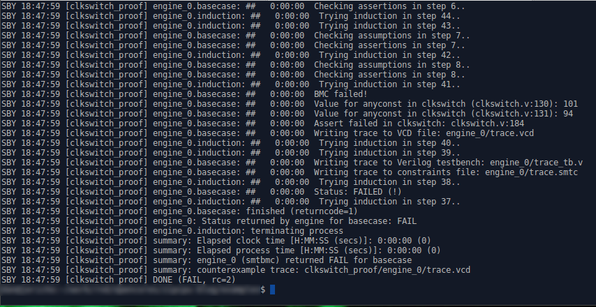 |
From this, we determine that our assertion from line 184 failed.
always @($global_clock)
	assert((!a_sel)||(!b_sel));
What happened?
If you look near the bottom of the SymbiYosys output, you’ll see a line identifying a counterexample trace. We can use this trace to find out why our proof didn’t work. This trace is shown in Fig 5 below.
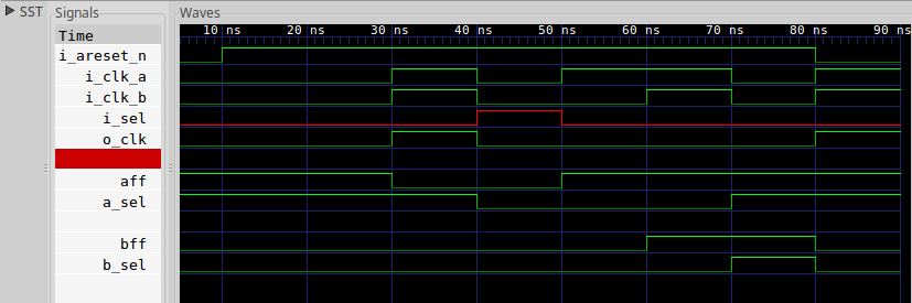 |
If you look closely at the penultimate time step, between 70ns and 80ns,
you’ll notice that both
a_sel and b_sel are true at the same time. This should never happen!
This violates all of the properties we are hoping to get from this clock
divider.
Looking closer, you can see that i_sel (shown in red) didn’t simply change
from selecting clock A to clock B. Instead, it started out requesting clock
B, suddenly switched to selecting clock A, and then immediately
switched back before the synchronizers could settle. Such a signal on
then i_sel select line would defeat the purpose of our clock
switch,
so it’s not really all that reasonable.
On the other hand, if we assume that i_sel won’t change until the clock
transition is complete, then we get a lot farther:
	always @($global_clock)
	if ((f_past_valid)&&($past(i_sel))&&(!a_sel))
		assume(i_sel);

	always @($global_clock)
	if ((f_past_valid)&&(!$past(i_sel))&&(!b_sel))
		assume(!i_sel);
As another way we might express this, we might insist that anytime there is
a change propagating through the synchronizers then i_sel will be
held constant.
	always @($global_clock)
	if ((a_sel != aff)||(b_sel != bff))
		assume($stable(i_sel));
Getting this design to pass induction requires some additional properties. For example, we can’t allow the design to be transitioning in both rails at the same time.
	always @(*)
	if (aff != a_sel)
		assert(bff == b_sel);

	always @(*)
	if (bff != b_sel)
		assert(aff == a_sel);
With these changes the design passes, proving our first criteria–that the outgoing clock only ever changes on an input clock edge. We also have a meager assurance that the outgoing clock will not be faster than either incoming clock. Perhaps we should examine the third criteria, and see how this switch works when swapping?
As you may recall, our third criteria was whether or not we could
switch from one clock to the other or back again.
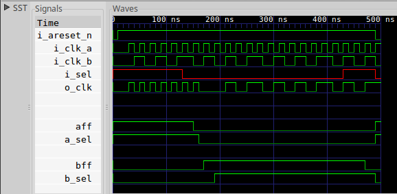
To see whether or not we met this criteria, we’ll need to run
SymbiYosys
in its cover mode. Our
script
has a cover task defined within it that does just that. The result is two
generated clock traces that illustrate how clock transitions might happen.
The first trace shows that a design can switch from a faster clock to a slower clock.
 |
The second trace, on the other hand, shows the clock switching from a slower clock to a faster clock.
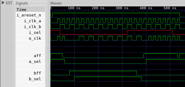 |
But what about the idea of a failsafe clock? Didn’t we say that one reason for using a clock switch is to be able to have a failsafe clock, where if one dies then the other one picks back up?
This particular design doesn’t support a failsafe clock.
If A is the failsafe clock, and B stops transitioning, then you
can’t switch from B back to A using this
design
since b_sel depends upon both a positive and a negative transition from
clock B.
Even though this clock switch design doesn’t offer a failsafe capability, you should now understand the tools necessary to prove that your own design, perhaps even one with a failsafe capability, would work—but only in an ASIC design of course! (Remember, the clock switch is not appropriate for an FPGA design for the reasons given above.)
Next Steps
Let’s think about what we just did. We just verified that a design with three asynchronous inputs “works”. This involved formally describing two dissimilar clocks with arbitrary phases and frequencies. These techniques apply well beyond this simple clock switch design. These techniques can be used in any asynchronous design component to verify that your logic is working as desired–in spite of whatever clock phases or frequencies might be given to it.
While working with asynchronous inputs isn’t common, there are times and places for doing so. I’ve already mentioned some examples above: an asynchronous reset, a serial port receiver, or perhaps a circuit that must read memory at one clock rate and feed a video stream at another rate. In all of these cases, knowing how to formally verify your component in spite of any multiple clock domains will be a valuable tool.
The next step in this short series on asynchronous logic will be to take Cliff Cummings’ asynchronous FIFO design, and apply the same basic formal verification steps we just applied above.
As an added bonus in this process, you should be able to then turn around and formally verify any modifications you need to make to his design to meet your particular design requirements.
And he said unto them, It is not for you to know the times or the seasons, which the Father hath put in His own power. (Acts 1:7)