
Taking a look at the TinyFPGA BX
 |
Some time ago, I wrote a review of the MAX-1000 FPGA board sold by Trenz. Today, I’d like to share my thoughts on another small FPGA development board: the TinyFPGA BX board.
If you’ve paid attention to the boards I like to purchase, I have a particular love for the smaller FPGA boards. Examples include the XuLA2-LX25, CMod S6, and the MAX-1000. These boards have all pin-holes for connections, running around the edges of the board. As a result, they either have very few peripherals, or these boards are rife with possibilities and just waiting for a fun electronics project. Your choice.
That said, this is probably a character flaw on my own part, because I’ve never been comfortable with a soldering iron. In reality, I shouldn’t be so concerned. At the extremely low cost of these small boards–and particularly the TinyFPGA BX, I can afford a soldering failure, or two, or perhaps even twenty, and I would quickly learn to be a better engineer as a result.
But let’s dig into the TinyFPGA BX, and see what we can do with something like this special board.
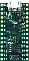
TinyFPGA BX
The TinyFPGA BX is a bare bones FPGA board. And, when I say bare bones, that’s exactly what you have. The board contains:
-
A power LED and a user controlled LED, and
-
A USB connection for programming the board
-
An iCE40 LP8k FPGA. This FPGA has 7680 4-LUTs, and is supported by a fully open source toolchain consisting of Yosys, ice-storm, and now NextPNR.
This iCE40 also has 16kB of block RAM.
When I tried to place the ZipCPU on this board, I quickly discovered I’d never be able to use all of that blockRAM for my CPU. Since the ZipCPU uses block RAM for more than one purpose (RAM, CPU registers, serial port FIFO, etc.), this effectively limited the size of the block RAM device available for the ZipCPU to 8kB.
That’s it.
Oh, I almost forgot, one of the great strengths of the board is that it has 24 digital I/O’s with which you can do whatever with. These I/O’s are brought out to pins on the edge of the board. Indeed, the strength of the board, as in other boards of this minimalist variety, lies in what you can do with these I/O’s.
What really sets the TinyFPGA BX apart, though, is how it handles the USB port.
TinyFPGA USB
Most of the programmable FPGA boards I have include an FTDI FT2232H chip connected to the USB port. This chip contains all the hardware necessary to both program the FPGA, and to connect a basic serial port from your FPGA design to your host computer.
Not so with the TinyFPGA BX. This is perhaps the biggest thing that sets the TinyFPGA apart from other FPGA solutions: it has no auxilliary chip for dealing with the USB.
Instead, the TinyFPGA requires FPGA design logic to communicate over the USB port–if at all.
I’ll be honest, before I discovered the TinyFPGA, I thought it was impossible to program an FPGA to communicate over the USB in a raw fashion like that. The TinyFPGA BX proves me wrong.
Here’s how this works:
-
When you power up the TinyFPGA, it immediately loads an initial “bootloader” design onto the board–much like a lot of microcontrollers, such as the PIC. This is not your user design. Instead, this is a design that will either load your design, or communicate with the board over USB, and so allow you to write a user design to the flash.
Fig 2. on the right shows the basic flash memory segregation. The first 165kB is used by this USB enabled boot-loader, the next 165kB is used by the user design, and the rest of the flash is available to your design.
 |
-
Using the TinyFPGA BX python tools, you can communicate with this bootloader and load your design into the next 165kB of flash memory.
-
Then, when you are ready and with the TinyFPGA plugged in, a USB command can be sent to the TinyFPGA to cause it to switch to the user design. This uses the iCE40 WARMBOOT primitive to cause the iCE40 to load a new design from a non-zero address within flash memory.
Once complete, your user design starts running. If your design doesn’t have USB capability within it, then you won’t have USB connectivity again until you restart the FPGA.
-
Ever after, the bootloader will load your design after waiting a second or two on startup.
-
To return to the bootloader mode, you either need to press the reset button, pull power from the FPGA, or issue your own command to the WARMBOOT primitive from within your own design to cause the FPGA to reload itself from the zero address.
All of this is to say that the TinyFPGA doesn’t really provide the same functionality that the FTDI chip did. Under this design concept, you cannot load a design onto the TinyFPGA without also loading it onto the flash first. There is no usable JTAG port to directly load the FPGA apart from loading it into the flash, or to debug the FPGA using vendor tools. Further, if you want a USB console port to your board, then you may need to design and and add it yourself.
It’s a pretty neat design concept. Better yet, it’s all open source! You can look up how the TinyFPGA does it, and then modify that design for your own purposes.
Practical Consequences
There are, however, some practical consequences of both the design concept and the hardware on the board.
-
Because loading your design onto the board requires a design already loaded onto the board, you’ll need to be careful not to erase, overwrite, or otherwise damage the bootloader design.
If you do, you haven’t quite bricked your board. However, you will then be stuck trying to reload the bootloader design back onto the board using the SPI pads (not pins, nor pin holes, but pads) on the back of the board.
While this may sound scary, the reality is that if you are going to be soldering or otherwise wiring this board into your own project somewhere, then you already have the skills to do this–even if it is a hassle. Indeed, if you look at the underside of the board, you’ll be able to see small pin-prick indents in the pads there, showing you where pins were used to connect to the design to load the flash initially.
If this is still more than you bargained for, then Tindie sells a breakout board for the TinyFPGA BX for only $11 that should give you access to these SPI pins for this purpose as well.
-
If you want to USB enable your own design, there are some consequences. First, the USB bootloader requires about 1k LUTs out of a board containing only 7.6k LUTs in the first place. Placing this bootloader, or other USB design, into your FPGA design will limit what you can do with your own design.
-
The really ugly part of this setup is that neither nextpnr nor arachne-pnr support multiple clock timing-driven placement (yet), nor does the icetime timing checker within the icestorm toolkit. Think this through. The USB design used by the bootloader runs at 48MHz. It is very much wed to this speed, and it would be difficult to change it. If your user design doesn’t run at 48MHz, you’ll be stuck either using the proprietary tool-chain or waiting for dual-clock support in nextpnr. (Arachne-pnr, though maintained, is no longer under active development.)
Just to give you a feel for timing, my own ZipCPU runs at 100MHz on a Xilinx Artix-7. It runs at 80MHz on a Spartan 6. It runs at 50MHz on an iCE40 HX8k. It runs at 25 MHz on the iCE40 LP8k found within the TinyFPGA BX. (icetime gives the design a 30MHz maximum clock speed.) Without being able to route my design for two separate clocks, my design will not have USB support.
Or would they? The ice40 boards do have an
SB_IOprimitive that provides support for a DDR capability …
What does this mean for me?
First, the small block RAM space on the chip is too small to hold the newlib C-library. Hence, if I want to run Hello World I’ll need to store as much library code as I can in the flash. I’ll need to be extra careful that, in this process, I don’t affect the bootloader. In addition, Hello World will need 2 wires dedicated to my USB-UART PMod, just so I can see the result and interact with my design–assuming that I can’t get a USB console to work.
I’m also very thankful that the TinyFPGA BX (now) supports all the wires necessary for QSPI flash! That will help to help keep the CPU speed up there, in spite of the non-pipelined CPU configuration (the only one that would fit).
TinyFPGA and FPGA Hell
The TinyFPGA bootloader has a USB protocol driver. This was one of the things that surprised me and caught my attention when I first discovered this board. In particular, I was curious to know how Luke Valenty built it. The USB specification is rather large and complex. I had to ask: What design method did Valenty use to get this interaction up and running?
So I asked. Valenty was more than happy to share how he had (or rather hadn’t) avoided FPGA Hell during his design process.
Me: I notice the TinyFPGA BX design includes a USB capability. Can you tell my readers anything about how you went about building it?
Valenty:
Most FPGA boards use a dedicated USB interface chip to enable programming and communication between the FPGA and a host computer. The most popular choice is an FTDI chip. This chip costs as much as the FPGA itself! I had a goal of developing a small and cost-effective FPGA board and I really wanted to deliver. I have a lot of experience with USB, so I decided to implement the USB interface fully on the FPGA itself. The ICE40 FPGAs have a multiboot capability that allows for multiple configuration bitstreams to be stored in the SPI flash and loaded at will by the design. This allowed me to develop a USB bootloader in a similar way that microcontrollers can bootload themselves over serial or USB interfaces.
The plan was to test the design on the TinyFPGA hardware against a real USB host. I had no testbench for simulation nor did I have any formal assertions or assumptions. This was a terrible idea and I spent a lot of time debugging issues on real hardware and implementing workarounds in the original programmer software.
Me: I’m not a board designer myself, so I have the advantage of examining a canned FPGA design for the board I’m working with before I ever start. Even better, I can return to that design if I think there might be a hardware problem with the board I am working with.
As a board supplier, can you share anything about what it took to get a first initial design running on the board?
Valenty:
Because I didn’t have any simulation or formal verification environment, I had to do all my testing and debugging on the real hardware. This involved running tests on the board while connected to a USB host and spying out internal signals to extenal pins so I can capture them on my logic analyzer. Debugging issues required me to make educated guesses about what signals might help me to debug an issue and rerunning the test multiple times while capturing different groups of signals until the issue could be identified and fixed.
This was a long turnaround between seeing an issue, root-causing it, and verifying a fix. It took quite some time and long nights to get the bootloader working reliably on all platforms.
Me: Did you ever find yourself stuck in FPGA Hell while designing and building the bootloader?
Valenty:
Yes, in fact, any time I go back to the bootloader I have to be very careful how I make changes. I have since added a simulation test bench and suite of tests, but making changes is still quite difficult.
Me: Did you use any simulation or formal verification techniques?
Valenty:
Nope, and this was a major folly.
Me: Would you recommend this approach to others?
Valenty:
This is pretty much the worst way to go about developing a digital design. In the end I was able to get the bootloader to work very well, but I spent a substantial amount of time working through issues that would have been trivial to find with a simulation testbench and/or with formal verification techniques.
I am currently working on a rewrite of the USB core and bootloader using Migen and a unit test methodology. The design is broken down into small and simple components that are then unit tested individually to ensure they behave as expected. This process is proving to be far easier, less time-consuming, and is creating a more robust design. If Migen ever gets support for formal assertions and assumptions I would be very interested in trying them out.
Me: Finally, what do you see as the biggest selling point of the TinyFPGA over and above other FPGA boards that may be out there today?
The TinyFPGA BX board is great to me because it’s completely open and very small. You have a lot of freedom to use the FPGA in any way in which you feel without paying extra money for components or peripherals you are not using. It’s a great way to create new and unique projects that take advantage of the power of FPGA. The TinyFPGA Discourse server has some excellent examples of projects the community has come up with: link
Thank you!
Using the TinyFGPA
I hope I haven’t given you the wrong idea about the TinyFPGA above. It is designed to be a very minimalist iCE40 FPGA board. It fills that role quite nicely. Even better, it is supported by an entirely open source FPGA tool chain.
If this is your first project, then do be prepared to do some hand wiring to connect your favorite devices/peripherals to the board.
Others have already been very successful with this board. These users have proved that you can play pong, pac man, or even space invaders on the board. Still others have ported the picoSoC project including a picoRV RISC-V CPU to the board. In other words, it’s not so spare that you can’t do anything with it, but it might test your creativity. Hopefully that’s why you are in the market for a board like this in the first place.
Me? Well, it shouldn’t surprise you to know that I’m more interested in placing a ZipCPU onto the board.
Will the ZipCPU fit? Yes. With a special hardware multiply unit, the normal divide unit, together with the pipelined fetch unit and compressed instruction support, a minimum ZipCPU build uses 5437 logic elements out of 7680, or about 70%. Yes, I rewrote both the multiply and divide units to get the logic count this low. I could go lower if I wanted by removing some of these extra features. My goal, however, was to leave enough room at the end so that I could incorporate a USB based serial port. Sadly, I might end up waiting a while on that.
Perhaps I’ll just GPS enable my device instead.
Seest thou a man diligent in his busines? He shall stand before kings; he shall not stand before mean men. (Prov 22:29)