
Generating Pseudo-Random Numbers on an FPGA
At some point or other, when working with FPGAs, you will need a pseudorandom number sequence. Trust me, it’s just going to happen.
In my case it happened this last week. I needed to do some channel estimation, and I reasoned that a pseudorandom sample stream would make a nice input to the channel. Specifically, my ultimamte plan is to transmit pseudorandom bits out of an FPGA output pin at the fastest speed I can: 950 Mbps on my Artix-7 Arty FPGA board. I can then receive the bits at the other end of the channel, and examine them to get an estimate of the channel distortion. If all goes well, I should even be able to apply Shannon’s Capacity theorem to determine the maximum speed of the channel.
All I needed to get started was a source of pseudorandom bits.
One common source for pseudorandom bits in digital logic is a Linear Feedback Shift Register (LFSR). LFSRs are simple to build and so they are commonly used for this purpose. They have some wonderful mathematical properties associated with them, guaranteeing a certain amount of pseudorandomness. Be forwarned, however, the one thing LFSRs are not is cryptographically random/secure. Do not use LFSRs in place of a proper cryptographically secure sequence. That said, they are worth learning how to create and use.
Much of my System Identification project will need to wait for a later post. Until that time, I’ll be accepting gentlemen’s wagers (no money involved) regarding what this ultimate maximum speed will be.
Today’s topic though is just a simple discussion of how to implement an LFSR in Verilog. We’ll skip the worst of the mathematics, although I would recommend you look them up.
Basically, the idea behind an LFSR is that given a current register state, I’ll call it a “fill”, you can compute the next state via a linear combination of the bits in the current state. I’ll use the term “taps” or “polynomial” interchangeably to describe this formula–although you might need to dig into more of the mathematics to understand why.
In this post, we’ll discuss these registers and how to create them in Verilog.
Basic Math
Let’s start, though, by looking at some very simple math. This math involves the Galois Field having only two elements, 0 and 1. We’ll use the term GF(2) to describe this field.
If you are not familiar with what a field is in this context, it’s simply a mathematical abstraction of a number system based upon a set of values, together with the definitions of addition and multiplication defined on those values. The neat thing about fields is that much of the math you are already likely to be familiar with is based upon fields. For example, I’m going to guess that you are probably familiar with linaer algebra. Linaer algebra, though, is all based upon fields. Although I learned linaer algebra using integers, real numbers, and complex numbers, linaer algebra is actually based upon fields: arbitrary algebraic systems with a defined set of values, as well as two primary operations defined upon that set.
We already said today’s topic would focus on the field known as GF(2), and that this field contains the numbers zero and one.
What we haven’t mentioned are the two two mathematical operators that define this field: addition and multiplication. Both are used in the implementation of an LFSR.
The difference between the addition and multiplication operators you might be familiar with, and the operators defined by GF(2), is that the GF(2) operators are followed by a modulo two. Hence, the result will be a ‘1’ if the traditional addition (or multiplication) result was odd, or ‘0’ if it was even.
 |
If you look at the addition operator under
modulo two,
you’ll find the first couple values to be what you expect:
0+0=0, 0+1=1, and 1+0=1. Where things get a little interesting is when
adding 1+1 together. In the traditional integer arithmetic you’re likely
familiar with, you’d get a 2. In arithmetic over
GF(2),
you need to take the result
modulo two,
and so 1+1 results in zero, as shown in Fig 1.
Think about that operation again for a moment: 0+0=0, 0+1=1, and 1+1=0.
That describes an
exclusive or operation, or XOR.
 |
We’ll do the same thing for multiplication. In this case, multiplying numbers from the set of zero and one will only yield the result zero and one, so you might not notice the modulo two. Then, when you look at the results as shown in Fig 2, you’ll quickly see that multiplication over GF(2) is nothing more than a bitwise-and.
Given these two operators, let’s define a bit-vector, sreg, whose elements
are either zero or one—elements from
GF(2). We’ll also state that
this bit-vector has an initial value given by INITIAL_FILL. In a similar
manner,
we can construct a linear operator, T(x), that can be
applied to sreg to yield a new or updated value for sreg at the next
time-step. This operator will be defined by another vector, TAPS, but
we’ll come back to this in a moment. For now, just remember that any
linear operation on a finite set can be represented by a matrix–another
fact we’ll come back to.
In pseudocode notation, an
LFSR
just applies the linear operator to the current sreg value over and over
again.
sreg = INITIAL_FILL;
while(!armageddon)
	sreg <= T(sreg);
A key thing to point out, though, is that any linear operation on the all
zeros vector will always return the all zeros vector, hence T(zero)==0. As
we go along, we’ll need to be careful to keep sreg from becoming zero.
What makes
LFSRs so special
is that as you apply this linear operator, the bottom bit will appear
to be pseudorandom. If you
choose your linear system well, an N bit shift register will walk through
all possible 2^N-1 combinations before repeating–generating 2^(N-1)
ones, and 2^(N-1)-1 zeros along the way. You do need to be aware, though,
not all linear systems have this property. Those that do are said to
create Maximal Length
Sequences.
These maximal length
sequences, however,
tend to be well known, and tables even
exist
containing examples of
LFSRs
that will generate anything from short
pseudorandom sequences
all the way up to very long ones.
Ok, I promised not to get deep into the math, but it is important to understand that LFSRs implement a linear operation on a bit-vector. These linear operations can be represented as a matrix operation–but only if the linear system described by the matrix follows the rules of GF(2).
Galois
As the wikipedia article on LFSRs explains, there are two forms of expressing
LFSRs. The first
is a Galois form, the second is known as the Fibonacci form. Both will yield
the same sequences, although their initial parameters, INITIAL_FILL,
and their TAPS values will be difference from one form to the other.
(Don’t worry, we’ll define these more formally in a moment.) Pictorially, a
Galois shift register
implementation
looks like Fig 3.
 |
Let’s let the number of stages in this register be LN, and the initial
value of all of the stages given by INITIAL_FILL. The last item needed
to implement a general purpose Galois shift register
implementation
are the coefficients of the multiplies shown in the figure above. We’ll
call these the TAPS–mostly because they “tap-into” the shift register
sequence when one, and ignore it when zero.
parameter	LN = ... ; // the size of your bit-vector
parameter	[(LN-1):0]	TAPS = ..., // some value in your design
				INITIAL_FILL = ... ;// Another design parameter
Looking at Fig 3 again, you can see an input going through
several (LN) stages
(Flip-flops)
of processing to create an output. That output is then
fed-back to affect the stages along the way. Notice also the adds and the
multiplies. These are the adds
(XOR)
and multiplies
(AND)
we discussed in our last section.
The multiplication values are given by the TAPS of the
LFSR. They do
not change during sequence generation.
The mathematicians will describe the TAPS as the coefficients of a
polynomial in GF(2).
These coefficients can either be a one or a zero–as with everything in
GF(2).
As we mentioned above, specific
choices
will yield maximal length
sequences.
If you would rather, though, I tend to think of TAPS as just a particular
N bit binary vector.
One of the reasons why I wanted to point out, in the last section, that an LFSR is nothing but a linear operator over GF(2), is that it allows us to write out this formula as a series of linear equations.
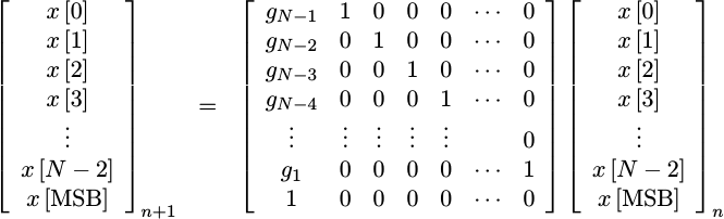 |
In this form, I’ve used g_1 through g_(N-1) to represent the taps. The
bit vector, x, has N bits to it ranging from x[0] through x[N-1] or
x[MSB]. This equation provides the formula for calculating the next
bit vector, x, from the last one. It’s worth noting that the entire
matrix is nearly upper right triangular, save for the g coefficients in the
first column.
Okay, so that’s the operation we want to perform. Now, let’s finish building it.
In pseudocode, I’m going to represent the x’s in a register I’ll call sreg,
and the g’s will be our TAPS bit-vector parameter.
The other value of interest is the INITIAL_FILL. For a maximal length
sequence, the only
restriction on the INITIAL_FILL is that it cannot be zero. Any other
value is allowed. This INITIAL_FILL will determine your starting point in
the random sequence created by the
LFSR.
You may also have noticed the “input” in Fig 3. We’ll set this to zero for today’s task. Setting it to another value has the effect of creating a feed-through randomizer, rather than the pseudorandom number generator we are building today.
The code necessary to implement a Galois shift register can be drawn directly
from Fig 3. We’ll use sreg to describe the values in the register, so that
our output, o_bit, is just the LSB of sreg,
assign o_bit = sreg[0];On a reset, we’ll initialize sreg to our INITIAL_FILL. Likewise, we’ll use
the “global-CE” pipeline
strategy,
so nothing is allowed to change unless i_ce is also true. This will make our
circuit useful for
DSP
tasks that need to run synchronously at data rates other than our clock rate.
always @(posedge i_clk)
	if (i_reset)
		sreg <= INITIAL_FILL;
	else if (i_ce)
	begin
With that aside, our logic is straight-forward. On every clock, we move all
the bits forward by one step. If the LSB is a one, we add
(XOR) the
TAPS vector to our state vector as the bits step forward.
		if (sreg[0])
			sreg <= { 1'b0, sreg[(LN-1):1] } ^ TAPS;
		else
			sreg <= { 1'b0, sreg[(LN-1):1] };
	end
Note how we checked for a 1 bit in the bottom bit of sreg. This is how to
implement the multiply. If the bottom bit is a zero, then the TAPS times
zero will be the zero vector which will not affect anything when added. On
the other hand, if sreg[0] is a 1, we’ll add the taps to our result.
The astute observer may note here that TAPS[LN-1] must be a one, or the
most significant bit (MSB) will be trivially zero.
Incidentally, this version of an LFSR is really easy to calculate in software, and its C++ equivalent is given by:
class	LFSR {
	// ... LN is given by 8*size(unsigned) below
	//
	// ... define INITIAL_FILL, TAPS, etc
	//
	unsigned	m_sreg;

	LFSR(void) { m_sreg = INITIAL_FILL; }

	void	reset(void) { m_sreg = INITIAL_FILL; };

	int	step(void) {
		// Calculate the output value up front
		int	out = m_sreg & 1;

		// Shift the register
		m_sreg >>= 1;

		// Use the output value to determine if the TAPS
		// need to be added (XORd) in
		m_sreg ^= (out) ? TAPS : 0;
		return out;
	}
}
If you look hard through the Linux kernel sources, you’ll even find an implementation of this algorithm within them. . There, though it’s used to implement a Cyclic Redundancy Check (CRC) and so their input isn’t zero.
You can find a copy of the code for the Galois LFSR on Github, as a part of my filtering repository.
Fibonacci
The other
LFSR form is
the Fibonacci form. The Fibonacci form of an
LFSR
is mathematically equivalent to the Galois
LFSR,
save that the outputs are calculated in a different manner, and the TAPS
need to be “reversed”. The diagram in Fig 4 shows the basic form of the
Fibonacci LFSR.
 |
In this figure, it’s the intermediate stages whose values are added (XOR‘d) together to produce an update value that is then added (XOR‘d) to the input.
In many ways, this makes an ideal form for implementing an
LFSR
on an
FPGA:
The feedback bit is usually calculated from just a small
number of taps (2-4) into the shift register, making it fit within a single
LUT quite easily.
Another unique feature to this form is that the values in the shift
register aren’t modified between when they are originally calculated and
the output–making it possible to see then next LN output bits by
just examining the shift register state. (We’ll use this in our next
post on
LFSRs,
showing how to generate more than one bit at a time.)
As with the Galois LFSR, the Fibonacci version also implements a linear system. This time, though, it has a different structure.
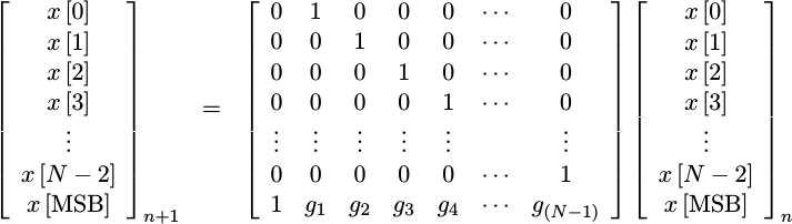 |
where the MSB is the feedback bit above.
When it comes to implementation, the initial implementation steps are the same as with the Galois implementation.
always @(posedge i_clk)
	if (i_reset)
		sreg <= INITIAL_FILL;
	else if (i_ce)
	begin
The difference is what you do to determine the next output bit. When using
the Fibonacci form, we take an inner
product between or
bit-vector, sreg, and our TAPS vector. This is nothing more than a point by
point multiply (AND),
followed by summing
(XOR)
all of the results of the multiplies together to create the new high order
bit. As before, we’ll hold the “input” to zero, and so we get the following
formula
		sreg[(LN-2):0] <= sreg[(LN-1):1];
		sreg[LN-1] <= ^(sreg[(LN-1):0] & TAPS);
	end
It’s not often that you get a chance to use an
XOR
reduction operator, however
this is one of those times. Note the expression ^(sreg[..] & TAPS). The
^ in the front of this specifies that all of the values in sreg[..] & TAPS
are to be added together, in a
modulo two sum–just
what we need to do here.
This isn’t the only way to build a Fibonacci LFSR within an FPGA. For example, this Xilinx app note discusses how to implement an LFSR using the shift register logic blocks within a Xilinx FPGA. Xilinx’s development is different from mine primarily because the shift register logic block that Xilinx depended upon does not support a reset signal.
You can find a copy of the code for this Fibonacci LFSR on Github, also a part of my filtering repository.
If you would rather see this example in VHDL, there is a VHDL version on OpenCores that you may find useful.
Test Bench
I’ve also placed a test bench for each of these two shift register implementations here and here. Since the two are nearly identical, I’ll walk through the salient portions of one of them only. For a more detailed description of how to build a Verilator based-test bench in general, please take a look at this article. The one thing we’ll do different here from many of my other projects is that we’ll call Verilator directly rather than using a subclass–just because our simulation needs for this component are so simple.
You’ll find this test bench starts out very simply. We call Verilator’s initialization routine, and declare a test bench based object upon our implementation.
int	main(int argc, char **argv) {
	Verilated::commandArgs(argc, argv);
	Vlfsr_fib	tb;
	int		nout = 0;
	unsigned	clocks = 0, ones = 0;
We’re also going to declare three more variables: clocks, nout, and ones.
We’ll use the clocks variable to count the number of clocks we use, to keep
from overloading the user’s screen with numbers. nout will be used to
help us place spaces in the output, and ones will be used to count the
number of ones in our output.
This test bench also
assumes that our result will be a maximal length
sequence. In this
case, there should be exactly 2^(LN)-1 unique outputs (clock ticks before
sreg equals one again), and 2^(LN-1) ones in those outputs. This will
be our evidence of success.
Our next step will be to start our core with a reset pulse.
	// reset our core before cycling it
	tb.i_clk   = 1;
	tb.i_reset = 1;
	tb.i_ce    = 1;
	tb.eval();
	TRACE_POSEDGE;
	tb.i_clk   = 0;
	tb.i_reset = 0;
	tb.eval();
	TRACE_NEGEDGE;
The TRACE_POSEDGE and TRACE_NEGEDGE are macros used to write the
simulation state to a
VCD file.
Once the reset is complete, we’ll assert that the shift register initial state
is 1. While this doesn’t necessarily need to be the case, setting
INITIAL_FILL to anything else within the
Verilog file
will necessitate coming back and updating it here.
assert(tb.v__DOT__sreg == 1);Finally, we’ll move on to the simulation itself. We’ll start out with
16384 clocks of simulation.
	while(clocks < 16*32*32) {
		int	ch;

		tb.i_clk = 1;
		tb.i_ce  = 1;
		tb.eval();
		TRACE_POSEDGE;
		tb.i_clk = 0;
		tb.eval();
		TRACE_NEGEDGE;
On each of these clocks, we’ll print an output bit to the screen. This should allow you to visually verify that the bits look random. We’ll place spaces between every eight bits for easier reading as well.
		ch = (tb.o_bit) ? '1' : '0';
		ones += (tb.o_bit&1);
		putchar(ch);
		nout++;
		if ((nout & 0x07)==0) {
			if (nout == 56) {
				nout = 0;
				putchar('\n');
			} else
				putchar(' ');
		}
		clocks++;
Finally, if the shift register value ever returns to our INITIAL_FILL of one,
then we know we’ve exhausted the sequence. We can therefore break.
		if (tb.v__DOT__sreg == 1)
			break;
	}
	TRACE_CLOSE;
In case you want to test for a really long sequence, the 16k clocks
won’t be enough. Rather than continue to fill your screen, the
test bench
just quietly continues crunching here.
	while(tb.v__DOT__sreg != 1) {
		tb.i_clk = 1;
		tb.eval();
		tb.i_clk = 0;
		tb.eval();

		ones += (tb.o_bit&1);
		clocks++;
	}
As a final step, let’s compare the number of clocks we used in our output to determine whether or not the test bench was ultimately successful.
	printf("\n\nSimulation complete: %d clocks (%08x), %d ones\n", clocks, clocks, ones);

	const int LN = 8;
	if ((clocks == (1<<LN)-1)&&(ones == (1<<(LN-1))))
		printf("SUCCESS!\n");
	else
		printf("FAILURE!\n");
}
Of course, since I’m posting this, I’ve already proven it …
Conclusion
There you go! That’s all there is to building an LFSR and demonstrating that it works.
Sadly, though, neither of our implementations today was sufficient for my channel estimation problem at 950MHz. Even if I could run this logic that fast, the rest of my logic wouldn’t be able to keep up. As a result, we’ll need to come back to this topic and see if we can’t build an LFSR that produces multiple outputs in parallel.
Still, LFSRs are a fundamental DSP tool, that’s easy to implement within an FPGA. Feel free to try yourself!
I returned, and saw under the sun, that the race is not to the swift, nor the battle to the strong, neither yet bread to the wise, nor yet riches to men of understanding, nor yet favour to men of skill; but time and chance happeneth to them all. (Eccl 9:11)