
Introducing the ZipCPU v3.0
It’s time to announce a new version of the ZipCPU: ZipCPU v3.0!
For reference, here’s how the ZipCPU’s development has taken place over the years:
ZipCPU v0.1
Way back in the beginning, the ZipCPU had four bit opcodes and only 16x16-bit multiplies. It truly had a very limited instruction set. That said, the instruction set design was too limited to be very functional.
This original instruction set didn’t even last a half a year.
ZipCPU v1.0
The ZipCPU, v1.0, had 32-bit bytes and no octet level access. If you wanted to read or write an octet (8bit value) in memory, you needed to read a 32b word, modify the 8b value within it, and write the 32b word back.
As a result, the ZipCPU, v1.0, did not have C library support.
ZipCPU v2.0
ZipCPU v2.0 provided 8-bit byte support, better compiler support, and full C-library support. The instruction set also included changes to the supported condition codes as well.
Now: Announcing ZipCPU v3.0
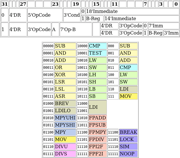
The good news is that the ZipCPU’s instruction set, as shown in Fig. 1, has not changed as part of this release.
 |
Although there have been (essentially) no changes to the instruction set with this release, it feels like everything else associated with the ZipCPU has changed:
-
This upgrade started with a core refactor, so that the ZipCPU could support more than just the Wishbone bus. As a result, the ZipCPU can now support Wishbone, AXI-Lite, and (full) AXI.
-
The new memory interfaces are now bus width independent, allowing the ZipCPU to work on buses larger than 32-bits. Indeed, it’s since been used on 64-bit and 512-bit buses quite successfully.
-
The core refactor led to better formal proofs, since the memory components can now be verified independently.
-
The DMA has also been rewritten for bus width independence. This rewrite provides even more capabilities along the way.
-
The debug port has been rewritten. This change is the one really necessitating a new major release, as it won’t even appear to be backwards compatible with prior releases. Instead of two registers, the rewritten ZipCPU debug port is now accessed via 33 registers: a control register and one debug register address per each of the 32 internal registers.
-
The companion core configuration file has been replaced by parameter settings at the CPU wrapper level. Parameter names have been formalized across wrappers, so common names configure common capabilities.
-
The ZipCPU now has its own simulation infrastructure for CPU level testing. This new infrastructure makes it possible to 1) test multiple configurations of the CPU, 2) test the CPU in multi-processor environments, 3) verify that the clock can be stopped and restarted, 4) verify the ZipCPU in both Wishbone and AXI configurations, 5) verify the lock instructions, and 6) verify the CPU’s new debugging port. This new simulation infrastructure also includes the ability to measure test coverage.
-
In perhaps the only downgrade of capabilities, the NOOP/SIM instructions NEXIT and SEXIT have lost their ability to exit a simulation with a given exit code.
-
Finally, the ZipCPU has the ability to stop its clock if necessary. Using this outside of the simulator will likely require hardware level support, so for the time being this may be a simulation only capability.
Put together, these are enough changes to warrant a new major release.
Let’s take a moment to discuss these changes.
Expanding the Bus
Perhaps the one reason driving this upgrade more than any other was the bus, both in width and in type. I needed to test a variety of AXI peripherals I was building and wanted (needed, really) a CPU that could speak both AXI and AXI-Lite. Some of these peripherals required bus sizes wider than 32-bits. Worse, the prior version of the ZipCPU’s core included the memory ports within the CPU core itself forcing the CPU to be Wishbone only.
This proved to be a verification nightmare. It meant that, in order to verify the ZipCPU’s core functionality, I needed to verify the ZipCPU against every possible memory interface it might have.
To make matters worse, which memory model the ZipCPU used was determined not by parameter, but by macro. This made the ZipCPU harder to configure or adjust in any design.
The fix was to refactor the ZipCPU. In the process, the interfaces to the prefetch, and the interface to the memory unit, were both standardized as shown in Fig. 2 below.
 |
The ZipCPU core was then verified against a pair of formal interface specifications, as were the instruction fetch and memory units. This made it possible to formally verify those units separate from the ZipCPU core.
The refactor wasn’t quite seamless. AXI exclusive access required a different interface to the ZipCPU than Wishbone exclusive access (i.e. bus locking) required. In Wishbone, all you need to do is hold the cycle line high between any two accesses to do any sort of “read-modify-write” routine. In AXI, on the other hand, any “read-modify-write” routine won’t know until the write return whether the sequence was successful or not. Then, if the sequence was not successful, the “read-modify-write” routine needs to be repeated. To add this new capability, the core now provides the AXI module the instruction pointer at the beginning of any “read-modify-write” sequence. If the “read-modify-write” sequence then fails, the memory module returns as if it were returning from a “load into the program counter” access causing a jump to the beginning of the sequence.
The good news is that, once I had the AXI interface I needed, I could then test and demonstrate ASIC IP using this approach. As a result, I’ve used this upgraded ZipCPU to test both a NOR flash controller and a hyperRAM controller using my Arty board, as well as an ONFI flash controller (via simulation only). This has provided me with the valuable ability of debugging system software entirely in simulation–and thus being able to answer why the device did (or did not) respond as expected.
Upgrading the DMA
Some time ago, someone contacted me to ask if I’d be willing to work with them to build an “ideal-DMA”. They had noticed that it seemed like every IP component they integrated into their SOC required a DMA, and so it felt like they had DMA’s running all through their SOC. Wouldn’t it make more sense, they asked, if we could just build one “better”/”ideal” DMA and not to keep building all these special purpose DMAs throughout their SOC?
 |
No, the deal didn’t go through. I didn’t have the hours to spare at the time, and we had some disagreements over the legal terms of working together. However, this did leave me asking the question, what would constitute an ideal DMA?
Then I needed to use my DMA with one of these wider bus sizes. Specifically, I was working on a project requiring a 512b bus width, and I use the DMA as part of the process of loading CPU memory images from flash to RAM in the first place. At this point, my one-32b-size-fits-all DMA just couldn’t connect to the bus. It needed to be upgraded. I no longer had a choice.
So, let’s think of all the lessons I’ve learned over the last couple of years using the last DMA. What would a better DMA look like? Specifically, a DMA is designed to move data around without CPU intervention. What kinds of data moves are required?
-
The most obvious requirement is for a
memcpy()type of data move, that moves memory from one location to somewhere else. Such a capability needs to move memory as fast as possible (it is a DMA, right?), and so it really needs to use the whole bus width.It also needs octet level alignment in order to be relevant–unaligned requests need to be expected, and handled appropriately.
-
What about peripherals? Consider audio peripherals, for example.
A microphone peripheral might capture 16b audio samples, generate an interrupt after each sample is captured, and then need its sample to be read and copied to memory.
A D/A peripheral might be similar: generating an interrupt whenever it consumes a sample and needs another. The DMA should then need to read the new sample from memory and write it to this peripheral.
In both cases, the data source address for the microphone peripheral, or the data destination address of the speaker, won’t change but the address in memory will.
To make matters worse, the audio peripheral might require 8b or 16b values which would be packed in memory. Hence the DMA needs to be able to read or write less than a full bus word at a time.
-
Years ago, I wrote a controller for an RGB based OLED peripheral. I demonstrated the capability of this controller by alternately placing the Gisselquist Technology logo and my own mug onto the display. In this case, the peripheral understood 32b command and data words, but the data had to be transferred one word at a time. An interrupt would then tell the CPU when it was time to transfer the next 32b word. To use a DMA, the DMA would need to wait for the interrupt, transfer the next word from memory to a constant destination address, then wait for the next interrupt again.
-
How about block peripherals? For example, I have an SDSPI peripheral which allows me access to an SD card via its (optional) SPI interface. The peripheral has two 32b data ports for transfers. Each port leads to a 512B FIFO, and the controller is expected to ping-pong between the two ports for speed.
Reading from the SD card will fill one of these FIFOs and then trigger an interrupt. At that point, a DMA needs to read (many times) from the same 32b address, form wide bus words together, and then write the results to memory.
Writing to the same FIFO is similar, only the interrupt works in a different fashion. The CPU would first call the DMA to transfer a block (typically 512 bytes) of memory to the data port FIFO. This block would need to be read at whatever the bus size is, and then packaged into 32bit writes to fill the FIFO. Once the transfer is done, the CPU should be interrupted, and the CPU can then instruct the SDSPI peripheral to write the information to the external SD card.
 |
From these requirements alone, what does a good DMA need to do?
-
(Optinally) Wait on an interrupt before starting any transfer. Which interrupt will need to be user selectable.
-
Transfer a given per-interrupt amount, perhaps less than the whole transfer.
-
Be able to read either 8b, 16b, 32b, or the full bus width at a time.
-
Be able to write either 8b, 16b, 32b, or the full bus width at a time.
-
Accessing peripheral memory may require that the DMA not increment the source or destination address, whereas accesses to memory will require both that the source/destination address increment and that accesses may (or may not) be aligned.
The new ZipDMA now offers all these abilities. It’s an awesome DMA capability.
You can see the basic structure of this new DMA in Fig. 4 below.
 |
Requests are made to the DMA, then sent to an FSM. The FSM then breaks those DMA requests into chunks. Remember, unlike AXI, Wishbone can only operate in one direction at a time. Therefore, all operations need to take place in chunks where data is first read, then written. In terms of the chunk processing itself, there’s a memory to stream processor to read data from the bus. This will read 8b, 16b, 32b, or the full bus width of data per clock cycle. Data are then packed by a gearbox prior to going into a FIFO. Coming out of the FIFO, the same data words are now unpacked into the user’s desired transfer width: 8b, 16b, 32b, or the full width of the bus. As the final per-chunk step, this data is placed onto the bus and written.
The biggest problem with this new capability? There’s only one ZipDMA. If it’s so good that every process needs it, there will be contention for it. The second biggest problem? This DMA capability is (currently) a Wishbone only capability. I don’t (yet) have an AXI version of it. Further work on this DMA will concentrate on making sure all of the various capabilities within it are properly verified–as I don’t yet have a good set of DMA focused test cases for that purpose.
A Better Debugging Interface
The original ZipCPU had only two registers for its in-hardware debugging interface. One register could be used to reset, start, stop, and step the CPU. This same register could be used to select which internal ZipCPU register the second register would access. Reads and writes to this second register would then either read or update the actual (selected) register within the ZipCPU. While this worked, it didn’t work well.
To illustrate the problem, consider Fig. 5 below.
 |
Reading any register from this interface required two accesses, and therefore two round trips through the debugging bus to the FPGA.
This interface struggled when I tried to debug ZipCPU programs over my serial port “debugging bus”. The debugger wanted the ability to read all of the ZipCPU’s registers. The two register interface then required that I first write the to the first register, that write then needed to complete, then I would read the data register, and that read would need to complete, all before I could move on to reading the second CPU register. That required two round trip transactions just to read one register, or sixty four round trip transactions to read all of the CPU’s registers. (There are 16 supervisor register and 16 user registers.)
This could take a long time over a serial port.
My debugging bus has another type of read command: one where you can read multiple sequential addresses in a row. This operation only requires sending the request (read thirty two 32b registers) and then waiting for the results. There’s no requirement for a round-trip handshake in the meantime. Instead, any handshaking is complete once the entire operation is complete. The CPU just needed a minor upgrade to provide enough addresses on the bus to do this.
You can see how this operation is different in Fig. 6 below.
 |
Even better, I formalized how the CPU was to respond to accesses. Debug register reads shouldn’t need to stop the CPU–that way you can monitor registers while the CPU is running, at the risk of reading an incoherent set of registers. This might be useful to know that the CPU is running, or where it might be in its processing. Bus writes, on the other hand, do need to stop the CPU.
Upgrading the Simulation Environment
The original ZipCPU’s purpose was to be absolutely as light on resources as possible. However, depending on the project, the “lightest resource” CPU might have too little power. I therefore quickly learned that the ZipCPU would need the ability to expand or adjust its area to fit the available area, while optimizing the CPU’s speed in that area. Example configurations might include whether or not the CPU used caches, or just very simple data accessing routines, whether the hardware supported multiplies via hardware-specific DSP elements, whether an all–RTL multiply was required, or whether the CPU should be built with no capability for multiplies at all. All this led to an early on requirement that the ZipCPU needed to be highly configurable.
My original approach to all this configurability was to create a separate configuration file containing a set of macros in it. The CPU’s configuration would then depend on if or how those macros were configured. I also had a separate project, one I called ZBasic, which would be used to test the CPU. Within the ZBasic project was a piece of CPU testing software that could then be used to test whether each of the CPU’s instructions worked. All of this put together worked great for testing a single configuration–the one described by the macro file. However I kept running into problems where I’d port the ZipCPU to some piece of hardware or other and it wouldn’t work. Perhaps I had made some change some time earlier, and only tested other configurations to prove that change. Whatever the cause, I was often left debugging the CPU in hardware–the one place you don’t want to debug the CPU.
As it turns out, it takes some engineering thought to build a test setup that can check all configurations of a highly configurable CPU.
Version 3.0 of the ZipCPU comes with such an infrastructure. I’ve written about it before. It centers around a Perl script and a file describing a series of tests. Each test specifies a canned configuration, a piece of CPU software, and one of two environments: a Wishbone environment and an AXI environment. Each test can also include any parameter overrides, so the default environments can be overridden for the test. I override these defaults, for example, to adjust the bus width for non-32bit bus testing. All told, there are 105 tests that take just over an hour to run under Verilator, or just over five days when using Icarus Verilog.
Simulation testing, however, is perhaps the one place where the ZipCPU’s instruction set is now less capable than before.
As background, the ZipCPU had two
special instructions, the NOOP and SIM instructions, that took specialized
arguments when run in simulation. In hardware, the NOOP instructions turned
into standard no-operation instructions, whereas the SIM instructions turned
into illegal instructions. That functionality alone left 22-bits of instruction
space which I could use for additional functionality,
from which I had carved out sub-instructions to write characters or even
register values to the simulation log. One special instruction would dump the
entire register set. Another special instruction, encoded as either NEXIT
(NOOP based) or SEXIT (SIM based) was supposed to cause the simulation to
end with a given exit code. It’s this xEXIT code’s functionality that’s
been lost.
The reason had to do with the implementation of these instructions. They were originally implemented by the Verilator C++ wrapper, and that wrapper required the ability to take a sneak-peek into the ZipCPU’s internals to know when to execute these instructions. This lead to two problems. First, the instructions would never work in a more traditional simulator that didn’t have or need such a wrapper–such as Icarus Verilog or a commercial simulator. The second problem was that the interface used by the wrapper kept changing. Since the features it depended upon weren’t standard Verilog but rather depended upon Verilator’s internals, the interface broke every time Verilator changed its internal data structure.
In the end, I resolved these problems by rewriting how the NOOP and SIM
instructions were handled, and the new rewrite was done entirely in Verilog.
Using Verilog only, I could guarantee that all Verilog compliant simulators
would correctly implement these instructions. However, I could not properly
implement the exit code requirement of the NEXIT and SEXIT instructions.
Hence, while the CPU has gained the capability of executing NOOP and SIM
instructions under a general purpose Verilog simulator, it has lost the
capability to exit the simulation with a specific exit code.
In many ways, this is a small price to pay for better interoperability between simulators, and the ability to simulate/test the CPU under a large number of configurations.
Clock Gating
One of the ZipCPU’s goals has always been low-logic. A truly low logic CPU should also be able to be a low-power CPU. In ASIC designs, low power often means clock gating, and the ZipCPU has had a plan for clock gating since the beginning.
Here’s how it works: the ZipCPU
supports two special modes, a HALT mode and a SLEEP mode. SLEEP will
cause the ZipCPU to stop executing
instructions until the next interrupt. HALT causes the
ZipCPU to stop executing instructions
at all, and thus to come to a complete halt until either the
debug port or an
external reset restarts the CPU. These modes were originally envisioned to
allow the clock to be stopped by the CPU.
This clock gating capability is now a reality–in simulation at least.
I’ve also now used clock gating several times, although never in actual hardware. The biggest lesson I’ve learned? The debug port must automatically restart the clock to handle requests. There’s been more than once when I’ve tried to load a program into the CPU externally from the debugging port, only to find out later that the reason the CPU was non responsive was because its clock was stopped. The next biggest lesson? Stopping the clock might lower simulation time, but this isn’t a given.
The end result of this work is that the CPU now has a program to test its ability to stop the clock.
Profiling
There was one more minor update to the ZipCPU, this one having to do with profiling.
Yes, I’ve profiled software–mostly benchmarks–running on the ZipCPU, although only in simulation. My current approach involves recording, for every instruction in a given program, both the number of times that instruction was executed and the number of clock cycles used to execute that instruction. The resulting data has done wonders for speeding up the CPU.
While I’ve been using this data for quite some time, my previous method of collecting it involved examining Verilator’s internal data structures to access it. While that has worked in the past, it forces me to update the ZipCPU every time Verilator changes their internal data structures. (This was the same problem I had with the simulation only instructions.) The solution is to create a proper external port, coming out of the ZipCPU, containing this data. It’s then there if you want to use it, or it can be ignored if you do not.
The ZipCPU’s simulation monitor program had the same problem, where it was also accessing values internal to the design. Such values tend to move or get renamed with Verilator updates. As with the profiler interface, this is easily solved by generating proper Verilog ports to the CPU containing references to these values for the monitor.
In both cases, I expect my updated solution to handling these values will need less maintenance as I use (and maintain) the ZipCPU over time.
Conclusion
As with any project, the ZipCPU remains a work in progress. It will likely remain so for the foreseeable future. This is a good thing. It means the CPU remains supported.
In the meantime, I’ve now used the ZipCPU on a variety of commercial projects. I’ve written about some of them. For example, it’s been used in a couple of SONAR applications, and I’m now importing it into a 10Gb Ethernet switch application. I’ve also used it to test, via both simulation and hardware, pre-ASIC IP cores. (I.e. IP cores designed for ASICs, but tested in FPGAs first.)
At present, the ZipCPU has two drawbacks that I’d still like to address in the future.
-
It still doesn’t have a memory management unit (MMU) to give it access to virtual memory. Worse, the MMU I designed years ago for the ZipCPU is now abandonware. It needs to be rebuilt. Since all of the internal interfaces have changed between the core and the memory components, the MMU’s required interfaces have changed as well. Worse, the ZipCPU’s core infrastructure may also need to be adjusted so that it can handle page faults. For example, what happens in a compressed instruction if the second half of the instruction suffers from a page fault? At present, compressed instructions do not need to be, and therefore cannot be restarted mid-instruction.
This upgrade will be required before I can truly run Linux on the ZipCPU.
The good news is that I don’t have any applications that require such an MMU at present.
-
Although the ZipCPU supports AXI, it doesn’t really do so by the book. AXI is, by the book, little endian whereas the ZipCPU remains a big-endian machine. Yes, it now has options to run in a little endian fashion, but the little endian options within the tool chain haven’t been tested, and so I have no confidence that they will work. What this means is that bytes within words are mis-ordered when using AXI. The ZipCPU will still write byte zero to bits [31:24], and byte one to bits [23:16] and so forth.
This has lead me to no end of troubles when testing AXI IP that is properly ordered. Not only that, but I now have an optimized software routine for byte-reordering–a patch, written instead of a proper upgrade.
I’ve imagined a third upgrade over the years as well: adding a floating point capability to the CPU. Moreover, I’ve reserved several instruction op-codes to support 32-bit single precision floating point operations. In hindsight, however, I’m not sure to what extent I would use these instructions even if I did implement them. I don’t normally use single precision floating point. I default to using double precision floating point. Not only that, but the ZipCPU will never be a hard core floating point processing machine. It just doesn’t fit that role. It will always be better as a fixed point system. Hence, floating point is no longer one of my goals for the ZipCPU.
This v3.0 release also marks the first time the ZipCPU has synthesized (with caches) on a Kintex-7 device with 200MHz clock!
Yes, the ZipCPU has been well used (by me), and remains well loved.
Every man's work shall be made manifest: for the day shall declare it, because it shall be revealed by fire; and the fire shall try every man's work of what sort it is. (1Cor 3:13)