
Fixing Xilinx's Broken AXI-lite Design in VHDL
Someone recently posted on Xilinx’s forums that they were having issues with their design. Apparently, the design was hanging on startup. When I asked if they had an AXI-lite slave within it, they shared their design with me. It looked an awful lot like Xilinx’s AXI-lite template design.
It’s amazing how often this design comes up.
This time, however, the design was written in VHDL. Since I don’t normally write about or discuss VHDL on the blog, I thought this might be an opportunity to examine a VHDL design. No, we won’t be examining VHDL today, just a VHDL design. Perhaps this will help someone new to AXI who isn’t (yet) familiar with Verilog.
Either way, let’s have some fun and examine Xilinx’s demonstration AXI-lite slave demonstration design, but this time in VHDL.
I’ll be using the commercial Symbiotic EDA Suite for this evaluation. The suite is now sold under the name “Tabby CAD Suite” by a company named YosysHQ, but I’ll leave those details for their marketing folks. Feel free to contact them and tell them I sent you.
 |
The setup for this verification proof is nearly identical to any Verilog setup, save that VHDL doesn’t really have a (supported) language for expressing assertions. (What about PSL? See the word “supported”.) For this reason, I’ll create a SystemVerilog wrapper around the VHDL design, as shown in Fig. 1 on the right. Within that wrapper, I’ll instantiate both the AXI-lite slave module under test, as well as the formal AXI-lite slave property set that we’ve discussed before. It’s all quite straightforward and (mostly) boiler plate. In this case I needed only five properties at the top level in order to get the design to pass induction.
The first thing to note about Xilinx’s VHDL design is that, yes, it’s still broken.
 |
Indeed, Xilinx’s AXI-lite VHDL design uses the same logic as their AXI-lite Verilog design does. Register for register, it’s hard to see a difference between the two designs.
How to recognize your design is broken
Let’s suppose, however, that you didn’t have any formal tools. How could you tell this design is broken?
After formally verifying many AXI-lite designs, it’s gotten really easy for me for me to spot the same bugs that keep taking place over and over. Indeed, there are just a couple things I look for and then I can spot most of these bugs (now) by eye. Here are two quick checks.
AxVALIDshould (somehow) depend upon(not xVALID) or xREADY
This is really the big criteria, and the one Xilinx’s
design
fails. Because AXI allows
backpressure, at some
point when the return channel is stalled, such as when
RVALID and (not RREADY),
the source channel will have to stall as well. This applies to both read
and write channels.
So, let’s look at Xilinx’s AXI-lite slave
design
and see if ARREADY somehow depends upon either not RVALID or RREADY.
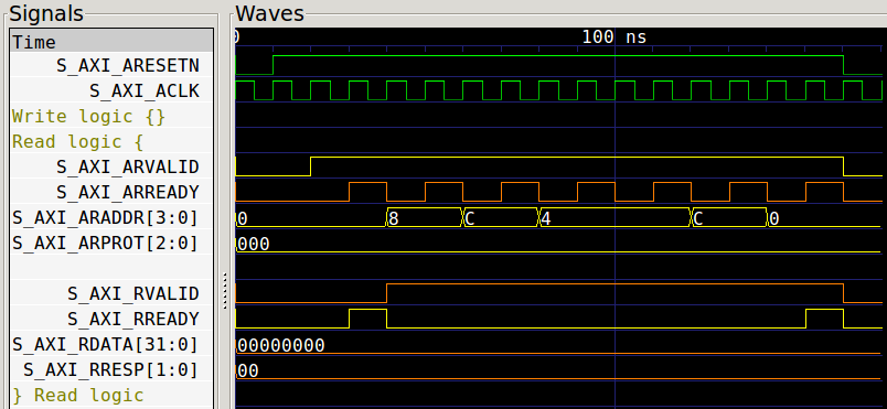
The answer is: it doesn’t. Here’s what their axi_arready logic looks like:
	-- Implement axi_arready generation
	-- axi_arready is asserted for one S_AXI_ACLK clock cycle when
	-- S_AXI_ARVALID is asserted. axi_awready is
	-- de-asserted when reset (active low) is asserted.
	-- The read address is also latched when S_AXI_ARVALID is
	-- asserted. axi_araddr is reset to zero on reset assertion.

	process (S_AXI_ACLK)
	begin
	  if rising_edge(S_AXI_ACLK) then
	    if S_AXI_ARESETN = '0' then
	      axi_arready <= '0';
	      axi_araddr  <= (others => '1');
	    else
	      if (axi_arready = '0' and S_AXI_ARVALID = '1') then
	        -- indicates that the slave has acceped the valid read address
	        axi_arready <= '1';
	        -- Read Address latching
	        axi_araddr  <= S_AXI_ARADDR;
	      else
	        axi_arready <= '0';
	      end if;
	    end if;
	  end if;
	end process;
Do you see any references there to S_AXI_RVALID? How about to S_AXI_RREADY?
How about any other signals related (somehow) to one or both of those two
signals?
No, you didn’t. That’s because it’s not there.
This design is broken. We’ll come back to this in a moment to fix it.
- Transitions should only be made on
xVALID and xREADY
When using AXI, nothing happens unless both the valid and ready signals are asserted on the given channel at the same time. While the formal tool doesn’t detect any more bugs in this slave, let’s still take a moment to look at some of the logic within it.
For example, what about the slave’s internal write enable signal?
slv_reg_wren <= axi_wready and S_AXI_WVALID and axi_awready and S_AXI_AWVALID;Have you ever wondered what would happen if this were only partially true?
I mean, what would happen if S_AXI_AWVALID && axi_awready && !S_AXI_WVALID?
What would happen is that the write address channel would accept a transaction
and the design would go downhill quickly. In one design I remember, one
with a lot of activity, every following write transaction was issued to the
wrong address–much like you might expect. Of course, the other possibility
is that the design might just hang.
Indeed, this is why, in my own
EasyAxil design,
I created a combinatorial signal, axil_write_ready, and fed this to both
the AW and W
skidbuffers:
	assign	axil_write_ready = awskd_valid && wskd_valid
				&& (!S_AXI_BVALID || S_AXI_BREADY);
When I built the
EasyAxil design
without skidbuffers,
I did roughly the same thing–only I registered the axil_write_ready
signal–something we’ll do here in just a moment.
On the other hand, if you are familiar with
Xilinx’s design,
you might quickly answer that axi_awready is the same as axi_wready,
and neither would be true unless S_AXI_AWVALID and S_AXI_WVALID were both
already true. Okay, so let’s go back and ask, then, why are axi_awready
and axi_wready separate signals if they’re equivalent?
Let me go one farther: this design won’t even set axi_awready unless
both S_AXI_AWVALID and S_AXI_WVALID are both true. So … why do we need
to check for S_AXI_AWVALID and S_AXI_WVALID a second time?
Let’s come back to this when we clean up the write logic further down.
The problem is worse on the read side. Consider the read enable signal.
slv_reg_rden <= axi_arready and S_AXI_ARVALID and (not axi_rvalid) ;Now, ask yourself, what would happen if axi_arready and S_AXI_ARVALID but
axi_rvalid were also true? In that case, the master would believe a request
had been made, but this slv_reg_rden signal would never go high. This would
become a nasty bug.
Here you can see the same condition repeated again when setting axi_arready.
if (axi_arready = '1' and S_AXI_ARVALID = '1' and axi_rvalid = '0') thenThis time, there’s a second problem: the author intended to use the same
logic as the slv_reg_rden signal, but wrote out the logic instead. That
means that if you ever have to fix this logic, you’ll have to do it multiple
times. In this case, it would be better to replace this logic with
slv_reg_rden and then only fix it once.
Let’s therefore take this as an opportunity to correct Xilinx’s demonstration design.
Fixing the read side
At this point, you should know the problem: in the presence of any backpressure, Xilinx’s design will drop requests. This will cause the bus to freeze, which will then cause your design to hang. The CPU will stop. To make matters worse, the debugger will also lock up. You will be unable to get any diagnostic information using either the system bus or the CPU.
This is nothing more than a recipe for FPGA Hell.
I’ve already pointed out the root cause of the problem above: the
design
never checks for S_AXI_RVALID = '1' and S_AXI_RREADY = '0' when adjusting
S_AXI_ARREADY. As a result, it accepts requests into the design even when
it will be unable to return a response.
Let’s start by fixing that.
As it turns out, the fix is simple. All we need to do is to adjust a single line. Instead of,
if (axi_arready = '0' and S_AXI_ARVALID = '1') then
		-- indicates that the slave has acceped the valid read address
	axi_arready <= '1';
we’ll replace it with,
if (axi_arready = '0' and S_AXI_ARVALID = '1'
		and (S_AXI_RVALID = '0' or S_AXI_RREADY = '1')) then
	-- indicates that the slave has acceped the valid read address
	axi_arready <= '1';
Voila! This design will now pass a formal verification check.
No, it’s not a great design. At best, this design will only ever get 50% throughput.
 |
While not great, at least it will now pass a formal property check. That also means that it won’t hang your design anymore, and you’ll be back to being able to use the CPU debugger to debug your software.
If we wanted to go further, we could do one better by dropping the read
latency by one clock cycle. We can do this by holding axi_arready
high until a request becomes available. One small change to axi_arready
and we’re there.
if ((axi_arready = '0' or S_AXI_ARVALID = '0')
		and (S_AXI_RVALID = '0' or S_AXI_RREADY = '1')) then
	-- indicates that the slave has acceped the valid read address
	axi_arready <= '1';
else
	axi_arready <= '0';
While we are at it, we should also adjust the slv_reg_rden logic. The
original logic.
just didn’t make any sense:
slv_reg_rden <= axi_arready and S_AXI_ARVALID && (not axi_rvalid);As I mentioned above, what happens when
axi_arready and S_AXI_ARVALID and axi_rvalid? With the new axi_arready
logic above, however, we’ve guaranteed that axi_arready will only be set if
axi_rvalid is also low. Therefore, we can replace this logic with,
slv_reg_rden <= axi_arready and S_AXI_ARVALID;For completeness, we should also remove any further references to
S_AXI_ARVALID and axi_arready and simply replace them with slv_reg_rden.
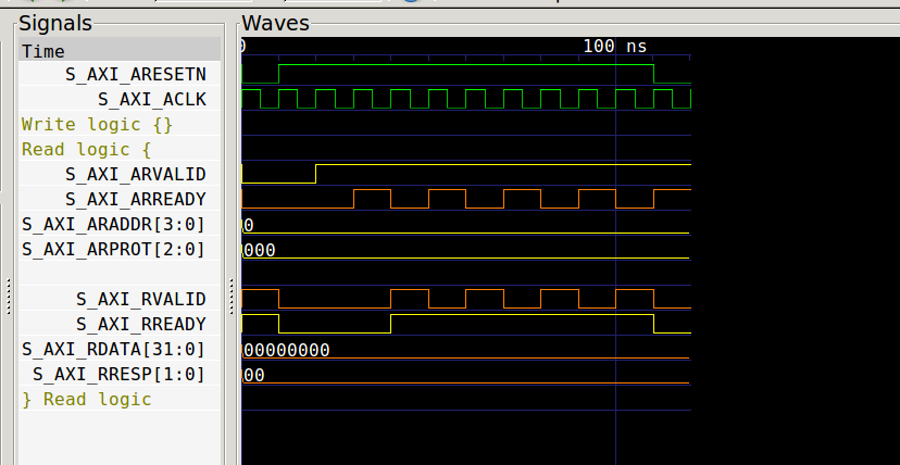
You can see the performance of this updated design in Fig. 4 below.
 |
The astute reader might also notice that this new and updated axi_arready
signal looks an awful lot like not axi_rvalid. A quick formal check confirms
that, with the exception of the reset value for axi_arready, this is indeed
the case. I’ll leave that change to the student.
Rather than simplifying the read logic any further, however, let’s instead move on to the write logic.
Cleaning up the write logic
 |
One of the challenges I have when looking at a design like this is not making edits throughout the design. Sure, the one change above will “fix” the protocol violations, but we could do much better with the write path as well.
The design works, though, why would we want to change it? Other than for the simple fact that I’m an engineer and that’s what I do, I can think of several reasons why we might want to clean this up a little bit.
First, the write logic as provided only gets 33% throughput.
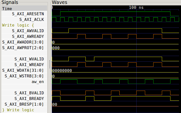 |
That’s pitiful.
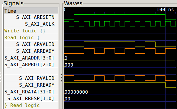
Back when I first ran the formal tools on Xilinx’s demo design, the write channel got 50% throughput–even though it was broken. Since then, Xilinx has fixed the protocol violations in the write channel. The only problem is, when fixing it, they dropped that 50% throughput number down to 33%.
In the process, they also added an aw_en register. Indeed, the existence of
this register will tell you if the write channel is from their “fixed” version
or not. Looking at Fig. 6 above, you can see that the design uses a minimum
of one clock cycle to acknowledge a write request, one clock cycle to return a
response, and then a third clock cycle to set aw_en. If we, instead, only
acknowledged a response when S_AXI_BVALID = '0', then we wouldn’t need
aw_en–we could use axi_awready–but I’ll get to that in a moment.
Third, did you notice that axi_awready and axi_wready used the same
identical logic? Sure, it works, but why would you have two registers to do
the same thing? Why not just use one? Indeed, if we just set S_AXI_WREADY
to axi_awready we’d get the same performance for less logic.
Finally, did you notice that S_AXI_BRESP is the constant "00"? Constant
expressions should be combinatorial expressions–not registered ones.
Let’s make a couple of quick changes to the write logic therefore.
-
As a first step, let’s remove the
axi_wready,axi_brespandaw_ensignal declarations. You can also removeaxi_rrespwhile you are at it, since that signal has the same problemaxi_bresphas. -
We can then set
S_AXI_WREADYtoaxi_awready, and bothS_AXI_BRESPandS_AXI_RRESPto"00". -
Now that we’ve dropped the
axi_wreadydefinition, we’ll also need to remove the process defining it. Remember, that process was producing a signal that was identical toaxi_awreadyanyway–so there’s no reason to use both.That’ll get us started.
-
We’ll then want to update the
axi_awreadylogic to remove theaw_enlogic, while still checking for any backpressure.That means we can change the first
ifcondition in the logic block below to one that doesn’t useaw_en, but also won’t be broken. Incidentally, we’ll also want to clearaxi_awreadyin all other cases. That means this original logic,
      if (axi_awready = '0' and S_AXI_AWVALID = '1' and S_AXI_WVALID = '1' and aw_en = '1') then
        -- slave is ready to accept write address when
        -- there is a valid write address and write data
        -- on the write address and data bus. This design
        -- expects no outstanding transactions.
           axi_awready <= '1';
           aw_en <= '0';
        elsif (S_AXI_BREADY = '1' and axi_bvalid = '1') then
           aw_en <= '1';
           axi_awready <= '0';
      else
        axi_awready <= '0';
can be simplified into the following:
process (S_AXI_ACLK)
begin
  if rising_edge(S_AXI_ACLK) then
    if S_AXI_ARESETN = '0' then
      axi_awready <= '0';
    else
      if (axi_awready = '0' and S_AXI_AWVALID = '1' and S_AXI_WVALID = '1'
		and (S_AXI_BVALID = '0' or S_AXI_BREADY = '1')) then
        -- slave is ready to accept write address when
        -- there is a valid write address and write data
        -- on the write address and data bus. This design
        -- expects no outstanding transactions.
           axi_awready <= '1';
      else
        axi_awready <= '0';
      end if;
    end if;
  end if;
end process;
where now I’ve shown the whole process.
Unfortunately, we can’t remove the clock cycle of latency from the write channel like we did with the read logic, since we’d then need to register either the write address or write data if one came early. Sure, that’s a valid design approach, but I’m trying to make as few changes to Xilinx’s template as possible. If you’d rather go all out to build a better design from scratch, then go for the EasyAxil design. That one will get you much better performance.
- Our next simplification will be to change the write enable signal,
slv_reg_wren,
slv_reg_wren <= axi_wready and S_AXI_WVALID and axi_awready and S_AXI_AWVALID ;to the much simpler axi_awready signal.
slv_reg_wren <= axi_awready;This, of course, doesn’t change how the design performs at all–it just simplifies the logic required to get it to perform in the first place.
But, shouldn’t we be checking here that
AWVALID && AWREADY && WVALID && WREADY?
In this case, it’s not required–we already did that when setting axi_awready.
If you aren’t convinced, then add an assertion to the wrapper:
always @(posedge i_clk)
if (S_AXI_ARESETN && axi_awready)
	assert(S_AXI_AWVALID && S_AXI_AWREADY && S_AXI_WVALID && S_AXI_WREADY);
You might notice that this slv_reg_wren signal is different from its read
equivalent. For the read equivalent, we only set slv_reg_rden high if
S_AXI_ARVALID and axi_arready were both true. Here, we are only checking
axi_awready. The difference is because axi_arready remains asserted
even when the design is idle, and so slv_reg_rden requires that we check
S_AXI_ARVALID as well whereas slv_reg_wren does not.
Conclusion
As I mentioned above, the resulting design isn’t that great. At best, it can only ever achieve a 50% throughput. AXI-lite is a much more capable bus than that. Indeed, we should be able to get 100% throughput from an AXI-lite slave, just like this design does. Doing so, however, requires a skidbuffer, and adding a skidbuffer would remove any remaining semblance of this being a Xilinx design in the first place.
There’s also a much more fundamental lesson to be learned here: just because a design comes from a vendor doesn’t mean it works. I’ve come across a lot of individuals on Xilinx’s forums who want to use Xilinx’s demonstration design if for no other reason than because it came from Xilinx.
Logically, this is called a “faulty appeal to authority.” The logic goes, 1) Bill is an authority, 2) Bill said X, therefore 3) X must be true. In this case, 1) Xilinx is an FPGA vendor, 2) that makes them an authority, 3) Xilinx provided this demonstration AXI-lite design, therefore 4) the demonstration design must work.
Unfortunately this logic is quite fallacious. Not only is Xilinx’s demonstration design faulty, but I’ve also been tracking flaws in two other demonstration designs, as well as in Xilinx’s AXI Ethernet-Lite IP, and now even in their AXI QuadSPI IP.
The obvious conclusion should be that you should think for yourself. Verify your own designs. Don’t trust an authority simply because he or she is an authority.
This reality applies to much more than just digital logic designs. It applies to the “science” regarding the Coronavirus–the same science that has been changing on a day to day basis over the last year. It applies to climate change. Indeed, I still remember when the climate scientists were warning of an impending ice age. It applies to the COVID “vaccine”, which you can choose to have injected into your bloodstream or not. It also applies to your relationship to the Almighty. In that final judgment day, you will stand before the Almighty. It won’t be your spouse, your boss, or your pastor, and it certainly won’t be your church. You will stand there alone.
Think about that, then live accordingly.
Though I speak with the tongues of men and of angels, and have not charity, I am become as sounding brass, or a tinkling cymbal. (1 Cor 13:1)