
Debugging a Cyclone-V
If you’ve read the description of Gisselquist Technology, you’ll remember that Gisselquist Technology is a services business. I use this blog and my demonstration IP cores to help attract customers. It also means that I don’t necessarily advertise all of the IP I’ve built on my projects page–since I’m not selling IP but rather my time and abilities. I prefer not to comment about the customers I work with, or what their various requirements are–that’s their business. I just provide them with a service.
However, a recent project I’ve been working on is worth commenting on from the standpoint of how to avoid FPGA Hell in a somewhat unique environment: the FPGA + ARM environment. This is probably all the more appropriate, as these FPGA + ARM chips are becoming more and more popular.
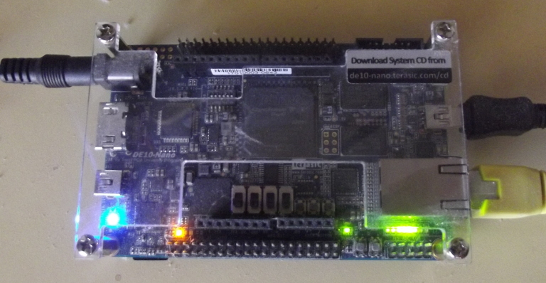
The project in question was a basic data acquisition system: control N A/Ds running at over a MHz in speed, and spit the results out over Ethernet. To make this project work, we chose to use the DE10-Nano as our processing device, shown below.
 |
This also marks my first experience with an FPGA + ARM type device, and what it takes to interface logic with an on-board hard processor, and I thought I might share with you some of my experiences and the lessons I learned.
General Project Structure
You can see the general structure of the project in Fig 2 below.
 |
In brief, the ARM processor has a number of buses available to it, within the chip, to communicate over. I chose the light-weight bus from the ARM to the FPGA for its simplicity–although I may revisit this decision later. I then used Qsys (now called the “Platform Designer” , although few tutorials have been updated since the name change) to connect my application specific design component(s) to an Avalon memory-mapped I/O bus.
This brings me to my own part of the design. For this application specific portion, I bridged from the Avalon bus to a Wishbone (WB) bus (all my legacy code was written for WB), and used AutoFPGA to assemble my design components together–assigning addresses and handling the bus interconnect within my own portion of the design.
This became my “debugging bus” as well for finding bugs within my design.
Further, the Platform Designer output is a big black box that I needed to create a wrapper for, connecting the ARM processor to the external system components–DDR3 SDRAM, GigE network, etc.
So what was the process for finding bugs?
My bug finding approach follows directly from my basic debugging philosophy. However, the basic philosophy really needs to be slightly updated, since I’ve started using formal methods. Basically, I followed the following steps:
 |
-
I wrote my design components and immediately “tested” them using the formal methods provided by yosys-smtbmc and the lint capabilities of Verilator. If any component didn’t pass muster from both of these tools, I didn’t even try it on the board.
This worked well for the bottom or “leaf” nodes of my design tree.
I also applied this method to a single non-leaf node, one that included my delay element as a sub-component. The purpose of this module was to segment the data into blocks, and to calculate the best exponent that could be applied to all of the samples in a given block. The timing of this module was critical, but it wasn’t simple to desk check–so the proof was important. Indeed, the success of the entire design depended upon this being done “right”. However, after cutting the proof down as much as possible, it still took a rough day of solid CPU computation to finish. This was rare among my proofs, as most completed within 5-20 minutes. Still, I needed the confidence of that formal verification proof and so I “paid” that price.
Neither did I apply formal methods to all of the design components. For example, one component contained three parallel FIFOs closely integrated together. Another component contained the entire signal processing chain (including the parallel FIFOs module). Neither of these components were formally verified, although I would’ve loved doing so–I just wasn’t certain I could manage the complexity required to do so. Hence these components were desk-checked, simulated, and tested on the hardware itself but never formally verified.
-
If the component passed formal verification and Verilator linting, I’d synthesize it and try it on the board. If it failed on the board, I’d add a wishbone scope to see what was going on. Since this was an AutoFPGA based design, adding or removing a wishbone scope was really easy to do.
-
This left me stuck in FPGA Hell only twice, and never for very long. First, I was stuck in FPGA Hell before I learned how to use the golden reference design properly. In these cases, the Angstrom Linux distribution I was using would never get past the boot-loader. Second, I would get stuck in FPGA Hell any time the system didn’t interact with the Avalon bus properly.
In the second case, my Verilator-based simulation rescued me nicely every time.
-
No, I did not use any Verilog based test-benches.
After having gotten a taste of formal methods, I’m not sure I’d go back to any other approaches if I didn’t need to.
The Crazy Bug
Ok, so … I did come across a rather “Crazy Bug”. You know, the kind that goes down in your memory banks as one that really stands out? The one bug in any project that takes you so long to find that you had to take notice of it? In my case, this bug took place across the interaction between the FPGA and the ARM processor.
For your sake, I’ll share what happened here, lest you get caught in the same bug yourself.
 |
After collecting samples from the
A/Ds,
those samples went through an initial signal processing chain.
Once that signal processing chain had finished working on the incoming
samples, those samples were placed into a
FIFO.
When the software running on the
ARM
was ready, it would call the
memcpy()
C-library routine
to copy samples from the
FIFO
to the user’s memory space. These processed samples were then sent
to a
socket
to be sent over
GigE
to a part of the system I had no control of. To make this happen, the
FIFO
was given the largest memory space I could afford, so that a vendor
optimized piece of code (i.e. the
memcpy())
could just copy the memory from the
FPGA
to RAM.
 |
I’m sure the actual
ARM
memcpy())
is a bit more complicated than the logic below, but the following is a basic
pseudocode outline of what the routine does:
// Example memcpy
void	memcpy(char *d, const char *s, size_t ln) {
	while(ln > 0) {
		*d++ = *s++;
		ln--;
	}
}
Only … that’s not I the behavior I observed.
Initially, all I knew was that the data coming out of the device was all jumbled, and I couldn’t tell why.
 |
If you’ve never had to deal with a data acquisition process like this, there’s one trick you need to have as part of your bag-of-tricks to find stream-based processing bugs–the counter. As shown in Fig 6 on the right, the counter runs along side the A/D controller. It increments with every sample. A user-configurable “switch” then selects whether the counter or the data is sent down-stream. If done right, you can then check the data values at the end of your processing stream, and you can tell whether samples were lost, corrupted, or worse–just by checking whether the ultimate sample values still had the one-up relationship present with a counter.
It was because this counter was not incrementing by one on every sample that I knew I had a problem.
So … I applied my scope to the bus transaction. My first thought was that I was somehow double or triple stepping my FIFO on semi-random reads, so I wanted to see what happened on a read from my FIFO. Using this scope, I discovered the FIFO was acting within normal limits. However, the values being read didn’t match the values in my code.
Ok, so I adjusted the scope and traced the problem up stream. Things looked good there.
So I adjusted my FIFO
so that it would return the address pointer instead of
the data. In this case, the
memcpy())’d
buffer came back finally in order with no problems, but the
scope
finally showed the problem.
 |
Instead of reading sample values 0, 1, 2, 3, 4, …, the ARM was reading sample values 0, 8, 16, 24, 1, 2, 3, 4, … and then quietly reordering the samples back into what it thought was the “correct” order. However, since the FIFO based device was producing values in order in spite of the out of order addresses, when the ARM rearranged the reads back in order–the result was the values in the buffer were now out of order.
Since knowing is half the battle, I now had two choices: I could fix the
memcpy())
routine by writing one of my own that didn’t read out of order, or
I could shuffle the memory back into order. I chose the former and wrote
my own
memcpy()), one where
I could guarantee that the reads would be issued in order.
This new version of code still read from my FIFO out of order.
As it turns out, it was the ARM CPU itself that caused the reads to be issued out of order, and then quietly placed the memory back in order on the other end. However, if I rearranged my own memory copy to never increment the “fake” address into the FIFO, then it finally read it in order.
I’ll say this much: I would’ve never figured this out without my Wishbone Scope.
Immediate Lesson’s Learned
As with any attempt to use a new piece of technology you aren’t familiar with, there will be hiccups. The Cyclone-V on the DE10-Nano was no exception. Indeed, it took me almost a month of grumbling and confusion to get off the ground before I discovered that, yes, the Terasic documentation did show me how to interact with this device. Here are some other frustrations I came across:
-
My first big frustration was the schematic I found online. It took me some time to realize that someone had posted a DE0-Nano schematic on an Intel DE10-Nano support web-page.
Sadly, despite posting a comment to this effect, this official Intel support page still contains a link to the wrong schematic.
In the end, I needed to destroy and then recreate my project in Quartus just to convince myself that I had gotten rid of all of the references to the wrong part.
-
My next frustration was that I couldn’t find an Altera “Libraries” reference.
Perhaps I’m spoiled: Xilinx offers a libraries guide that gives you instructions for how to interface with any of the hard components on the chip. Hence, if I need a PLL, I just put a reference to their PLL within my own code and off I go.
I couldn’t find a similar libraries guide for Altera. Indeed, I probably spent much too much time looking for it.
In the end, I just swallowed my aversion to working with GUI’s and built the PLL I needed using Platform Designer. Since resigning to use Platform Designer, it has handled all of my needs to date–I just hate using GUI’s: they are slow, and they can hide details where I’m not looking for them, etc. Although, looking over the Platform Designer generated data file in the end, it’s just an XML file–one that submits nicely to “diff”, and thus one I can use with git quite nicely.
-
My second problem had to deal with the “Golden H/W design” provided by Terasic for the board.
Looking through this design with Altera’s Platform Designer, I could easily identify a variety of things I didn’t need. I dumped these out of my project, and then cleaned up the result so that there were only the components I needed, and then built the project.
It didn’t work. The board would load and run the bootloader just fine. The bootloader would load my FPGA design, but would then fail to start Linux. Not knowing how to debug Linux loading to know what device was failing, how, or why, I just couldn’t tell why not.
In the end, I went back and rebuilt the Golden Design as provided, and then only modified it for my application. This worked.
-
I really dislike vendor code that doesn’t match my own high quality coding standards.
By this I mean two things. First, I use
default_nettype nonein all of my designs. It helps me avoid a whole variety of painful Verilog bugs. However, a bug in the Altera’s Cyclone-V IP would cause my design to fail if I tried to use this across my design.With a little bit of help from an amazing mentor, I managed to use
default_nettype noneat the top of my files, anddefault_nettype wireat the bottom and Altera’s broken code would still synthesize.I then got all kinds of warnings from their “working” IP. I mean, really guys, can’t you clean up your own IP? How can I tell if my implementation of your IP has problems if your IP fills the logs with warnings–when it works!? (Incidentally, Xilinx’s code isn’t any better, and Xilinx’s MIG-generated DDR3 SDRAM controller is a particular offender …)
The worst of these warnings said that I hadn’t mapped several pins properly, and yet the pin mapping tool wouldn’t let me do anything with these hardware-assigned yet somehow mis-mapped pins. As with the other warnings, these could be ignored, but how was I to know that when things weren’t working?
Again, building the Golden H/W Reference Design gave me some confidence, as I could then see that I still got the same warnings and yet for some outrageous reason, the Golden Design worked in spite of the warnings.
This blog is about debugging FPGAs, though, so what did I learn from that standpoint?
-
One mistake in the Avalon bus controller would lock up the device HARD.
If this happened, the only solution appeared to be pulling power.
The formal proof of the Avalon to WB converter created a bit of a false confidence for me: my design still locked up at times.
-
The first problem I had with my Avalon bus interface was that I somehow managed to assume within my proof that all transactions would be read transactions. The assumption wasn’t simple, and it wasn’t obvious, so I never realized what happened from a simple desk check.
In the end, I figured out what was going on via simulation.
When I went back to the formal properties, I realized I hadn’t created any “cover” properties, and that a simple “cover” property or two would’ve revealed this problem.
-
My next problem was when I mis-wired a bus component in AutoFPGA.
For a given peripheral, the WB strobe value is given by the overall wishbone strobe (a transaction request) logically
ANDed with the peripheral’s address select line. I had forgotten this address select line logicalANDon one component, and so that component was responding to EVERY transaction across the bus–with pretty catastrophic results.As with the prior problem, I found this pretty quickly … once I fired up the simulator.
-
-
Simulator? How …?
Yes. Exactly. I couldn’t simulate the ARM processor, the DDR3 SDRAM, the GigE network, the lightweight AXI bridge, or the AXI to Avalon memory-mapped I/O bridge, but I could create a Verilator-based simulation of the Avalon bus interface on down–to include simulating the A/Ds. That portion of the design was a fairly straight-forward AutoFPGA based implementation, and even though it wasn’t a full-design simulation, it was enough to simulate enough of the design to find many problems.
Given my experiences with an FPGA + ARM architecture, would I recommend it for others? As with any engineering decision, your choice will depend upon the requirements of your problem. However, I would have really struggled if this had been my first-ever design. Hence, I’d recommend beginners start with something simpler–such as a plain FPGA with an on-board (debuggable) soft-core CPU, before adding the ARM to the mix.
Conclusions
There’s more I could say, but this post is long enough as is. I’d like to be able to blog some more about the Avalon to WB bridge and how I managed to formally verify it, how easy it is to suddenly add a scope to a design using AutoFPGA, or indeed how powerful AutoFPGA is in general.
These discussions will sadly need to wait for a later day.
If we say that we have not sinned, we make him a liar, and his word is not in us. (1John 1:9)